DOI:
10.1039/D0RA00801J
(Paper)
RSC Adv., 2020,
10, 17217-17227
Room-temperature synthesis and CO2-gas sensitivity of bismuth oxide nanosensors†
Received
27th January 2020
, Accepted 12th April 2020
First published on 1st May 2020
Abstract
Room-temperature (27 °C) synthesis and carbon dioxide (CO2)-gas-sensor applications of bismuth oxide (Bi2O3) nanosensors obtained via a direct and superfast chemical-bath-deposition method (CBD) with different surface areas and structures, i.e., crystallinities and morphologies including a woollen globe, nanosheet, rose-type, and spongy square plate on a glass substrate, are reported. Moprhologies of the Bi2O3 nanosensors are tuned through polyethylene glycol, ethylene glycol, and ammonium fluoride surfactants. The crystal structure, type of crystallinity, and surface appearance are determined from the X-ray diffraction patterns, X-ray photoelectron spectroscopy spectra, and high-resolution transmission electron microscopy images. The room-temperature gas-sensor applications of these Bi2O3 nanosensors for H2, H2S, NO2, SO2, and CO2 gases are monitored from 10 to 100 ppm concentrations, wherein Bi2O3 nanosensors of different physical properties demonstrate better performance and response/recovery time measurement for CO2 gas than those for the other target gases employed. Among various sensor morphologies, the nanosheet-type Bi2O3 sensor has exhibited at 100 ppm concentration of CO2 gas, a 179% response, 132 s response time, and 82 s recovery time at room-temperature, which is credited to its unique surface morphology, high surface area, and least charge transfer resistance. This suggests that the importance of the surface morphology, surface area, and crystallinity of the Bi2O3 nanosensors used for designing room-temperature operable CO2 gas sensors for commercial benefits.
1. Introduction
Rapid advances in science and technology have resulted in a significant change in our lives. During these developments, myriad environmental problems which are responsible for global concern are stimulated. Gaseous contaminants released from industries and automobiles diffuse quickly over huge areas within a small period of time, causing atmospheric pollution that is accountable for acid rain, the greenhouse effect and ozone-layer depletion.1–3 In particular, it is now understood that the global warming is affecting on the eco-system and may result in disastrous consequences for life and property. CO2 is the main culprit and is permeating our daily lives as a dominant pollutant from transportation, industrial and agricultural activities, and is commonly used in biotechnological processes, as a fire retardant in air conditioning systems.4–6 Furthermore, it is also responsible for various health-related issues; its high concentration exposure causes problems such as dizziness or headache, which on long term exposure resulting in simple health issues such as breathing complications and oblivion.7–10 In the last decade, researchers are being actively engaged in monitoring CO2 gas sensors at low-concentrations and room-temperature to reduce its direct effect on global warming and other hazardous processes taking place around.6,10,11 The concentration of atmospheric CO2 gas is commonly measured using non-dispersive infrared sensors, which are based on electrochemical and thermal-conductivity detection principles.12,13 However, these sensor technologies suffer from various limitations such as bigger size, more weight, high cost, and restricted lifetime.4 Therefore, several alternative approaches for obtaining low-cost, room-temperature operation and stable CO2 gas sensors are being researched, including solid electrolyte (potentiometric), capacitive, or field-effect-transistor and metal oxide-based sensors.4,14,15 Metal-oxide-based CO2 gas sensors developed extensively in the past owing to their relatively honest working principle and easy employment as micro-electronic devices.16,17 Moreover, sensors of Bi2O3, SnO2, ZnO, La2O3, rare-earth metal oxides, and Ag-doped CuO, Al2O3 and SnO2 etc., and oxide-based materials envisaged for detecting and monitoring CO2 gas at low concentrations.15,18–24 However, in the majority of these cases, the change in the resistance/conductance is negligible at higher concentrations of CO2 gas. In contrast, the Bi2O3-nanoplate-based sensor demonstrated a significant sensing performance to CO2 gas with fast response/recovery time, which remained unchanged even up to the 11![[thin space (1/6-em)]](https://www.rsc.org/images/entities/char_2009.gif) 000 ppm level, suggesting that the study of crystal structure, surface area, and morphology on the gas-sensor performance is essential.15 The Bi2O3 endows promising applications in optical coatings, catalysis, gas sensors, photovoltaic cells, and microwave integrated circuits due to its unique bandgap energy, refractive index, dielectric permittivity, photoconductivity.25–29 Moreover, the synthesis of inorganic nanosensors with desired surface morphologies has great importance in mounting functional materials. So far, various nano/microstructures of metal oxides such as cubes, discs, flowers, polyhedrons, and sheets, etc., been synthesized by various chemical and physical synthesis routes. The change in the surface morphology of electro-active materials can significantly influence the gas sensing performance, since this phenomenon is greatly influenced by surface related properties, and different morphologies of same sensor can demonstrate various sensing performances.29b,c The intention of this article is to design different Bi2O3 nanosensors of different morphologies followed surface areas for room-temperature CO2 sensing applications.
000 ppm level, suggesting that the study of crystal structure, surface area, and morphology on the gas-sensor performance is essential.15 The Bi2O3 endows promising applications in optical coatings, catalysis, gas sensors, photovoltaic cells, and microwave integrated circuits due to its unique bandgap energy, refractive index, dielectric permittivity, photoconductivity.25–29 Moreover, the synthesis of inorganic nanosensors with desired surface morphologies has great importance in mounting functional materials. So far, various nano/microstructures of metal oxides such as cubes, discs, flowers, polyhedrons, and sheets, etc., been synthesized by various chemical and physical synthesis routes. The change in the surface morphology of electro-active materials can significantly influence the gas sensing performance, since this phenomenon is greatly influenced by surface related properties, and different morphologies of same sensor can demonstrate various sensing performances.29b,c The intention of this article is to design different Bi2O3 nanosensors of different morphologies followed surface areas for room-temperature CO2 sensing applications.
Herein, we focus our attention on the development of Bi2O3 nanosensors using low-temperature solid-state synthesis process. It has a slightly complex structure owing to its α, β, χ, δ, and ε polymorphs.30 To date, several methods such as electro-deposition, solvothermal deposition, chemical vapor deposition, atomic layer deposition, chemical deposition method, and successive ionic layer adsorption and reaction etc., have been successfully used to synthesize Bi2O3 of various nanosensors.31–38 In majority of the cases, single or plain morphology was identified, and the synthesis time was significantly lengthy. However, several researchers have appealed that the polymorphs of sensing materials, such as hierarchical, porous, or hollow, largely contribute to their sensing properties.39–41 Such structures offer a large surface-to-volume ratio that enables easy and fast electron transportation and a process of gas diffusion with an enhanced sensing performance.42,43 Therefore, monitoring the morphology of gas-sensing materials of different surface areas can be advantageous in improving the gas sensing performance.44
Considering the merits different surface areas, morphologies, and structures, in the current work, we report a direct and rapid synthesis of Bi2O3 nanosensors using poly-ethylene glycol (PEG), ethylene glycol (EG), and ammonium fluoride (AF) surfactants via a soft chemical method at room temperature.45 All these nanosensors of Bi2O3 were characterized for their crystal structure, morphology, surface area, and pore-size distribution measurements. Finally, room-temperature CO2-gas-sensing performance of the Bi2O3 nanosensors of different morphologies and surface areas are measured and reported.
2. Experimental section
2.1 Materials and methods
All the required chemicals were obtained from Sigma Aldrich and used as is without furthered purification: bismuth nitrate pent hydrate, (BiNO3·5H2O), nitric acid, (HNO3), hydrochloric acid (HCl), ammonium fluoride (NH4F), ammonium hydroxide (NH4OH), ethylene glycol (MW – 62.02), and polyethylene glycol (MW – 200). The pieces of glass substrate (Duran Group Inc., Mainz, Germany) were pre-treated chronologically with acetone, 2 M HCl solution, distilled water, and ethanol, for 20 min each to confirm uncontaminated surface. Furthermore, this glass-substrate was used as a substrate for decorating different nanosensors of Bi2O3 as thin-film nanosensors. All the selected gases used in the tests were collected from CryoGases Pvt. Ltd. Company, which is placed in Mumbai, (India).
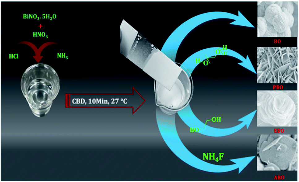
2.2 Synthesis of various Bi2O3 nanosensors
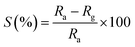
The experimental procedure for the synthesis of the Bi2O3 nanosensors has been reported in detail in our prior work.45 Various Bi2O3 nanosensors were synthesized without surfactant; in the presence of PEG, EG and AF; with surfactants at room temperature; and on a glass substrate; and these were named as Bi2O3 (BO), PEG@Bi2O3 (PBO), EG@Bi2O3 (EBO), and AF@Bi2O3 (ABO), respectively. In brief, 0.1 M Bi(NO3)3 was dissolved in 50 mL of double-distilled water, and a suitable amount of 1 M HNO3 was added to dissolve the Bi(NO3)3 to obtain a transparent solution. The dropwise addition of aqueous ammonia (30%) solution resulted in pH ≈ 8. The four identical beakers were arranged to tune the morphology of Bi2O3 and in order to tune the morphology of Bi2O3, the three surfactants mentioned above, i.e., PEG (1 wt%), EG (1 wt%), and AF (1 wt%) were added into above-prepared solutions separately, and no surfactant was added to one beaker, i.e., BO (see Scheme 2). Well-cleaned pieces of glass substrate were immersed in the above-prepared beakers placed at room temperature. Finally, 2 mL of HCl was added to initiate the oxidation reaction in each beaker. All of the reactions were completed in less than a 10 min deposition time, a heterogeneous reaction occurred and different Bi2O3 nanosensors of various morphologies were obtained on the glass substrate dipped in four different beakers. It should be noted that all of the sensor samples used for the physical as well as gas-sensor measurements were prepared without an annealing process. The physical elucidation and morphological analysis of all the Bi3O2 nanosensors were performed through various modern techniques (see ESI S1 for more details†).
2.3 Measurement of gas sensing properties
Scheme 1 presents a schematic view of the tentative experimental setup used for gas sensing measurements. For the sensing operations, the material coated on the glass substrate, (i.e., Bi2O3 was inserted in the electrical DC circuit and enclosed in a stainless-steel cylindrical chamber of 250 mL volume capacity).
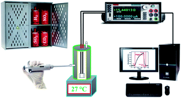 |
| | Scheme 1 Schematic representation of the gas sensor measurement setup. | |
The cylinder-shaped compartment consisted of a heater with a proportional-integral-derivative regulator to set the preferred temperature, if required was used. The specified amount of gas was inoculated into the sensing compartment, which was equipped with a mixing fan, in order to acquire the desired unchanging concentration of gas. For determining the electrical resistance of the sensor, a simple electronic setup was employed. In this system, the electrical resistance was first transformed to a DC voltage. Then, a computer-assisted six-digit Keithley source meter (model number 6514) system was used to allocate the digital data in computer via an RS 232 serial port. The response of the individual Bi2O3 gas sensor was examined46 using following relation.
| |
 | (1) |
where, the values of electrical resistance before (
Ra) and after (
Rg) contact between the samples and the analysis gas, respectively, at a stable working temperature (which is 27 °C in the present case).
3. Results and discussion
3.1 Role of surfactant in growth mechanism of Bi2O3 nanosensors
The surfactants act as coordinator and have a strong cross-linkage ability, thereby producing various morphologies.47–49 Initially, during the chemical reaction, seed nuclei may grow through different distinct steps such as nucleation, aggregation, and coalescence as microspheres of Bi2O3.45 The surfactants PEG, EG, and AF play critical roles in the development of various Bi2O3 nanosensors of different morphologies, which are summarized through the following reaction mechanisms (Scheme 2). The one without surfactant, i.e., BO can grow in a straight-forward manner as Bi(NO3)3·5H2O was liquefied in HNO3 and H2O with the addition of ammonia to upturn the pH ∼ 8, which was the source of Bi3+ (eqn (2)). The oxidation process was initiated in the solution after the insertion of the glass substrate and the addition of 2 mL HCl in the solution. The reactions were treated in the same beaker by attaching OH− to Bi3+ and creating [Bi(OH4)]− unstable complex (eqn (3)). Finally, H+ could attach to [Bi(OH4)]−in the precursor, thus resulting in Bi2O3 as given by eqn (4).| | |
Bi(NO3)3·5H2O → Bi3+ + NO3− + H+ + OH−
| (2) |
| | |
Bi3+ + 4OH− → [Bi(OH4)]−
| (3) |
| | |
2[Bi(OH4)]− + 2H+ → Bi2O3 + 5H2O
| (4) |
 |
| | Scheme 2 Schematic presenting the growth of various morphologies of Bi2O3. | |
PEG and EG are basic members of the glycol family. The key difference between these molecules is their chemical structure, where PEG has a polymeric chain. On adding the PEG surfactant in the solution containing Bi3+ ions (eqn (2)), the number of hydroxyl groups in a polymeric chain of a surface may be covered with Bi3+ nuclei owing to the presence of van der Waals forces between them and {O–[–CH2CH2–]n–OH}– bonding Bi3+ ions, and thus, [Bi{O–[–CH2CH2–]–OH}x](x−3)− would be obtained, which is known as an unstable intermediate complex (eqn (5)). Moreover, the reaction was processed in the same flask wherein, OH− was attached to the bismuth and [Bi{O–[–CH2CH2–]–OH}x](x−3)−, which is an unstable intermediate complex that becomes stable by forming [Bi(OH4)]− (see eqn (6)). Furthermore, H+ attacks [Bi(OH4)]− in the same manner to produce Bi2O3 as given in eqn (7).
| | |
Bi3+ + x{HO–[–CH2CH2–]n–OH} → [Bi{O–[–CH2CH2–]n–OH}x](x−3)− + H+
| (5) |
| | |
[Bi{O–[–CH2CH2–]n–OH}x](x−3)− + OH− → [Bi(OH4)]−
| (6) |
| | |
2[Bi(OH4)]− + 2H+ → Bi2O3 + 5H2O
| (7) |
where, EG is a simple linear molecule, and owing to a limited number of molecules, the growth of Bi
2O
3 is greatly restricted. Hence, the growth of an individual nanostructure is beyond control after the addition of the EG surfactant in the Bi
3+ ion solution (
eqn (2)). Therefore, the {O–[–CH
2CH
2–]–OH}
− group of EG, which is in contact with the Bi
3+ nuclei forms an unstable complex (
eqn (8)),
i.e., [Bi{O–[–CH
2CH
2–]–OH}
x]
(x−3)−. On attacking OH
− on Bi-nuclei, [Bi(OH
4)]
− is obtained, which, on attacking H
+ ions results in the formation of Bi
2O
3 (refer
eqn (9) and
(10)).
| | |
Bi3+ + x{HO–[–CH2CH2–]–OH} → [Bi{O–[–CH2CH2–]–OH}x](x−3)− + H+
| (8) |
| | |
[Bi{O–[–CH2CH2–]–OH}x](x−3)− + OH− → [Bi(OH4)]−
| (9) |
| | |
2[Bi(OH4)]− + 2H+ → Bi2O3 + 5H2O
| (10) |
As fluorine (F−) is a good promoter, AF plays as significant role in tuning the surface morphology of Bi2O3. The F− ions in all reactions act as a catalyst by attaching to Bi3+ (eqn (2)), and after the completion of the reaction, the ion is liberated (eqn (11)) to form [BiFx](x−3)−.50,51 With the reaction time, the concentration of OH− increases in the presence of F− ions in the solution. Moreover, F− can be replaced by OH− via coordinates with Bi3+ by forming [Bi(OH4)]− (eqn (12)). The presence of H+ in the same precursor can provide an easy entrance to [Bi(OH4)]− to obtain Bi2O3 (eqn (13)).
| | |
Bi3+ + xNH4F → [BiFx](x−3)− + NH4+
| (11) |
| | |
[BiFx](x−3)− + OH− → [Bi(OH4)]−
| (12) |
| | |
2[Bi(OH4)]− + 2H+ → Bi2O3 + 5H2O
| (13) |
3.2 Role of surfactant in obtaining Bi2O3 nanosensors
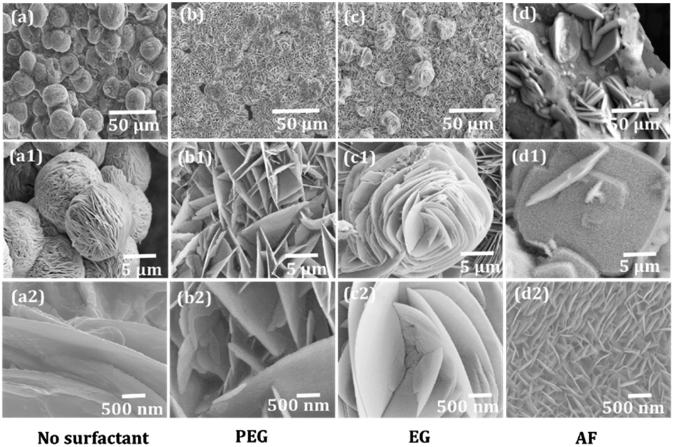
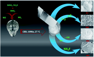
The FE-SEM images of Bi2O3 on a glass substrate as shown in Fig. 1(a–a2)–(d–d2) confirms moderate difference in surface appearance of the obtained Bi2O3, which suggests the importance of the surfactant type during particular Bi2O3 morphology growth. The surfactant, being an additive, aids in promoting the development to improve the density of the morphology.52 The Bi2O3 morphologies such as woollen globes, nanosheets, rose-type, and spongy square plates were obtained under surfactant-free, PEG, EG, and AF surfactant conditions, respectively.
 |
| | Fig. 1 FE-SEM images of BO (a–a2), PBO (b–b2), EBO (c–c2), and ABO (d–d2) recorded at different bar scales. | |
The surfactant-mediated nanosensors (Fig. 1a–d) of Bi2O3 accept the complete variation in the surface morphology. From Fig. 1, where (a–a2) are high-magnification FE-SEM images, it is observed that the woollen globes comprise several interconnected upright-standing nanoplatelets (Fig. 1a). Between these nanoplatelets of woollen globes, a hollow air cavity is evidenced (Fig. 1a2). Fig. 1b–b2 is inferred the platelet-type morphology of Bi2O3 with a PEG surfactant. These platelets were assembled to form a nanosheet-morphology (Fig. 1b). Among these nanosheets, substantial air voids were existed (Fig. 1b1). The higher magnification image proposed that the nanosheet-like microstructure is self-possessed of dozens of radially full-fledged 2D nanoplatelets (Fig. 1b2). After the combination of EG in the precursor solution, the growth of the rose-type Bi2O3 comprising loosely packed curly nanoplatelet arrays is identified (Fig. 1c–c2). These nanoplatelets were amalgamated with one another to form a rose-flower. In the presence of AF, the FE-SEM image of Bi2O3 confirms the spongy-square-plates view (Fig. 1d and d2). Several rectangular disks reside on the glass substrate. Each disk is made up of three morphologies, viz., up and downright standing and parallel to the edges of the respective disk. Nevertheless, their lengths are undecided, as they seem to be well linked to one another. The third morphology, i.e., parallel plates with inter-branched signatures is incredible. These are equivalent as specified above, and the FE-SEM outcomes support the well-ordered evolution of the Bi2O3 morphologies by only fine-tuning the surfactant additives. The presence of air-voids and the uniform debris-free character of the Bi2O3 morphologies would make them excellent sensor materials.
3.3 Structural elucidation
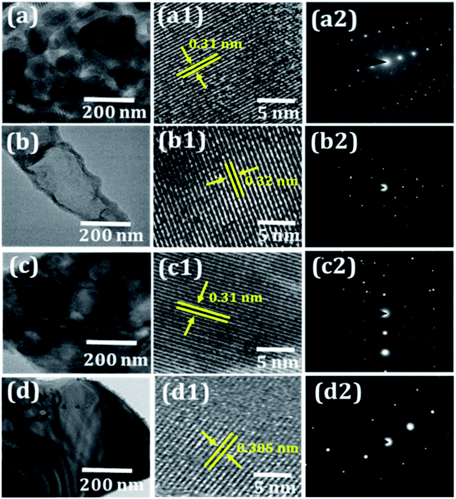
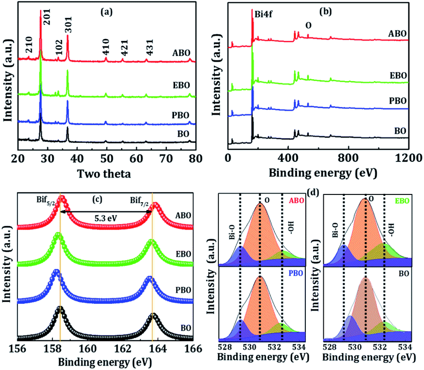
The elemental fixation shown in Fig. 2(a–a2)–(d–d2) suggests that the Bi2O3 nanosensors consist of uniformly distributed Bi and O elements with a 40:60 atomic composition ratio (see Fig. 2a2–d2). The EDX spectrum exhibits strong peaks of Bi and O at the appropriate46 energy levels (Fig. 2a2–d2). Furthermore, the high-resolution TEM images (Fig. 3) revealed that these nanosensors are composed of several polished nanoplatelets. The lattice fringes of all Bi2O3 nanosensors were dignified with the electron beam perpendicular to the surface of a nanoplatelet. The 0.31(±0.02) nm interplanar spacing between the neighbouring lattice fringes agrees to d-spacing of (201) plane from Bi2O3 (refer, Fig. 3a1–d1). The lattice data intended from the SAED pattern (Fig. 3a2–d2) of a casually chosen section of the nanoplatelets were in good agreement with the lattice parameters of β-Bi2O3. Both the HR-TEM and SAED measurements propose the growth of tetragonal β-Bi2O3 in the [201] direction.53 The presence of high-pitched and continuous lattice fringes is in agreement with the nanocrystallinity of Bi2O3 film sensors. The phase purity of the Bi2O3 nanosensors of different morphologies was investigated based on the XRD patterns (Fig. 4a). All the achieved reflection peaks were in worthy arrangement with the tetragonal β-Bi2O3 as per the 27-0050 JCPDS data file card. However, no evidence for impurity peaks was detected in the XRD pattern. The peaks indexed to the (210), (201), (102), (301), (410), (421), and (431) planes in the XRD patterns were very sharp and deep, which proposes a polycrystalline nature of the as-deposited Bi2O3 nanosensors. The strong diffraction peak found at 27.94 suggested that the preferential growth-orientation direction of Bi2O3 is (201).54
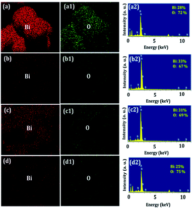 |
| | Fig. 2 Elemental scanning of Bi and O over the BO (a–a2), PBO (b–b2), EBO (c–c2), and ABO (d–d2) sensor surfaces. | |
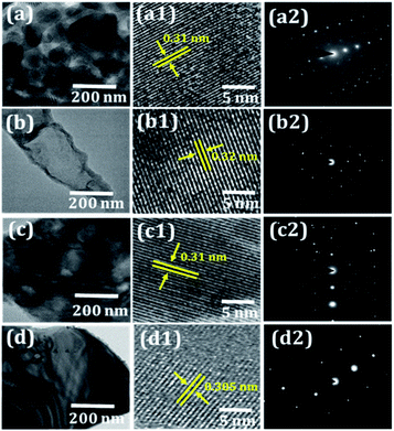 |
| | Fig. 3 (a–d) TEM images, (a1–d1) high-magnification HRTEM images, and (a2–d2) SAED pattern of BO, PBO, EBO, and ABO nanosensors. | |
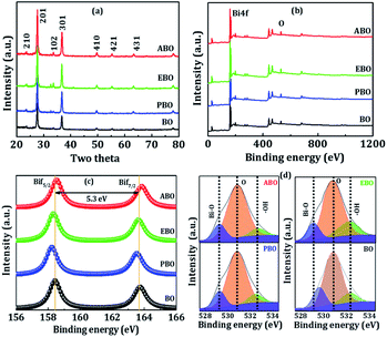 |
| | Fig. 4 (a) XRD, (b) full-range survey XPS spectrums of BO, PBO, EBO, and ABO nanosensors. Enlarged XPS spectra of (c) Bi4f, (d) O1s for BO, PBO, EBO, and ABO nanosensors. | |
The XPS analysis measures the chemical nature of each element present in the manufactured nanosensors of Bi2O3. Fig. 4b displays the survey scan, which clearly illustrates the presence of Bi and O at their corresponding binding energies in the manufactured nanosensors of Bi2O3, which indicates the non-appearance of impurities. In the survey scan, Bi4f showed a major peak with binding energy at approximately 160(±3) eV. The de-convoluted Bi4f region shown in Fig. 4c reveals the presence of bismuth metal along with all synthesized nanosensors of Bi2O3. After deconvolution, the Bi4f spectrum showed peaks at 158.3 eV and 163.7 eV for Bi4f7/2 and Bi4f5/2, respectively.55 Fig. 4d confirmed the high-resolution scan of the O1s state at a binding energy of 530.9(±3) eV, which after deconvolution, confirmed Bi–O, O1s, and Bi–O–H peaks at the binding energies of 529.7, 530.9, and 532.3, respectively.56 The detailed XPS analysis supported that these nanosensors are belonged to Bi2O3. The specific surface area and pore-size distribution measurements of the Bi2O3 nanosensors were achieved from the deposited powders, scratched from glass substrate, using N2-adsorption/desorption isotherms (Fig. 5c and d), (sequence check) wherein, the attendance of the H3-type hysteresis loop in the range of ca. 0.6–1.0 P/P0 approved the participation of the mesoporous-character Bi2O3 nanosensors57 (discussed later).
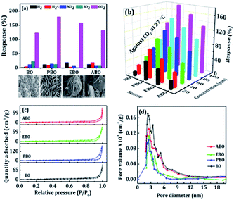 |
| | Fig. 5 (a) Gas selectivity (at 100 ppm), (b) response versus CO2 concentration of the BO, PBO, EBO, and ABO nanosensors at 27 °C. (c) Nitrogen adsorption–desorption isotherms and (d) BJH pore-size distribution plots of the BO, PBO, EBO, and ABO nanosensors. | |
3.4 Gas sensing study
A series of gases were used to demonstrate the room-temperature gas-sensing performance of the as-obtained Bi2O3 nanosensors. As shown in Fig. 5a, the responses of the as-obtained Bi2O3 nanosensors (i.e. BO, PBO, EBO and ABO) to CO2, H2, NO2, SO2, and H2S gases confirmed higher selectivity and sensitivities to CO2 gas over the other selected testing gases at their fixed 100 ppm level. Fig. 5b demonstrations the vibrant response of the Bi2O3 nanosensors for CO2 gas with a concentration order of 10, 20, 40, 60, 80, and 100 ppm wherein, the graphs are designed with an identical scale for quickly comparing the sensing responses. It is apparent that the response largeness is highly reliant on the gas concentration. The gas-sensing transients of the Bi2O3 nanosensors exhibited a smooth response/recovery behaviour. Speciously, the PBO-nanosheet-type sensor revealed a better CO2-gas-sensing response than that of the others. When the PBO nanosheet sensor was operated under 10 ppm CO2 gas, the response value was approximately 52%. As the CO2-gas concentration increased from 10 to 20, 40, 60, 80, and 100 ppm, the recorded responses were approximately 52, 80, 101, 118, 146, and 179%, respectively. The gas responses of the EBO rose-flower-type sensor under similar CO2 gas concentrations were 42, 63, 87, 105, 126, and 158%, respectively. The BO woollen-globe/ABO square-plate-type sensors were respectively 12/23, 26/40, 42/56, 60/71, 78/103, and 123/132%. The gas response of the PBO nanosheet-type sensor to 10 ppm of CO2 gas (52%) was higher than that of the BO woollen-globe (12%), EBO rose-flower (42%), and ABO square-plate-type (23%) gas sensors. Nevertheless, it is apparent that there are performance differences among the BO woollen-globe, PBO nanosheet, EBO rose-flower, and ABO square-plate-type Bi2O3 nanosensors in the case of CO2 gas. In all the cases, with the concentration of CO2 gas, the response to the CO2 gas increased. These outcomes indicated that the surface morphology of the Bi2O3 nanosensor has an impact on the CO2-gas-sensing performance at room-temperature (discussed later).
Fig. 5b displays the dynamic response of the Bi2O3 nanosensors towards CO2 gas with a concentration order of 10, 20, 40, 60, 80, and 100 ppm, where, the graphs were designed with an identical scale for rapidly matching the sensing responses.
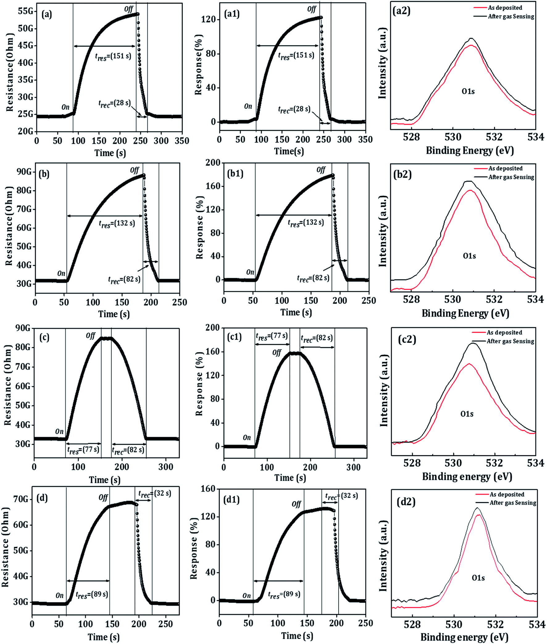
In order to further authorize the connection between the morphology of a Bi2O3 nanosensor and its gas-sensing performance, nitrogen adsorption/desorption measurements of the overhead four nanosensors were measured. As seen in the nitrogen adsorption/desorption cyclic curves in Fig. 5c, the adsorbed quantities of the BO, PBO, ABO, and EBO nanosensors were determined. In fact, the BET surface areas of these nanosensors were calculated to be 31, 58, 44, and 37 m2 g−1, which indicates a downtrend in the active surface area, suggesting the width and length may contribute to a huge surface area and, which results in a high sensitivity. The pore-size distribution curves (Fig. 5d) of these nanosensors proposed that the modest nanosensors diameter (∼52 nm) and density (∼283 mm−2) are linked to identical and appropriate pore size, which are significant factors for realizing mass transportation and an actual surface area. The average pore-size distribution maxima for the BO, PBO, ABO, and EBO nanosensors and average pore volumes were 5.16, 2.53, 2.87, and 3.89 nm, respectively. On comparing the Bi2O3 nanosensors, it is observed that a thin and sparse woollen-globe-type sensor produced a higher pore volume but a lower operative surface area, while a dense and thick nanosheet-type sensor contributed a smaller pore space and huge surface area. Only the reasonable diameter and uniform dispersal of these nanosheets could result in the production of suitable pore space with a huge surface area and, thus, can be more beneficial for using as sensing materials with a high sensing performance. It is noted that the BO, PBO, EBO, and ABO nanosensors exhibited an increasing surface area and decreased average pore-size, hence higher gas-sensing response. So, these outcomes exhibited that the surface area and pore size of the structures also contribute to the gas-sensing performance, which is in covenant with earlier arguments.58 When BO, PBO, EBO, and ABO nanosensors are wide-open to CO2 gas, Bi2O3 catalyses the oxidation of CO2. This reasons the electrons to become surrounded by the detached oxygen species that changes the electrical resistance to generate a well sensing response. The momentary gas-response time signatures of CO2-gas sensing for a 90% variation in the resistance from the original value are presented in Fig. 6a–d.
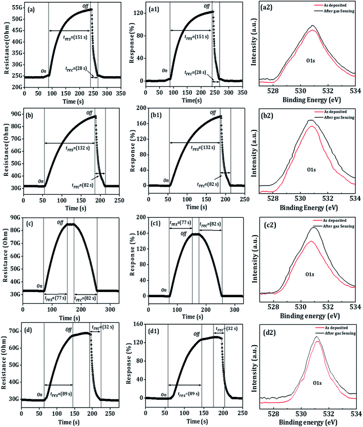 |
| | Fig. 6 (a–d) Transient versus time (at 100 ppm), (a1–d1) response versus time (at 100 ppm), of the BO, PBO, EBO, and ABO nanosensors, and (a2–d2), O1s XPS spectra of before and after CO2-gas sensing of the BO, PBO, EBO, and ABO nanosensors. | |
On exposing the CO2 gas to the BO, PBO, EBO, and ABO nanosensors, the resistance values were respectively increased from 24.36 to 54.26 GΩ, 31.68 to 88.46 GΩ, 32.87 to 84.42 GΩ, and 29.66 to 68.77 GΩ. The BO, PBO, EBO, and ABO nanosensors have demonstrated maximum response values of 123, 179, 158, and 132% at room-temperature and 100 ppm CO2 gas. The as-prepared Bi2O3 nanosensors of different morphologies followed surface areas confirmed room-temperature CO2 gas sensitivity over other gases which is attributed to the absorption of CO2 molecules leads to disruption of the hopping chains necessary for the Grotthuss mechanism and therefore, hinders proton transport, which in turn leads to increase the charge transfer resistance followed reduced proton diffusion which is not processing for other gases (see Fig. S2†). The response/recovery time depends on the rate of diffusion of the gas molecules onto the sensor surface or related reaction rate between the target gas molecules with the sensor elements. The responses of the BO, PBO, EBO, and ABO film sensors at 10–100 ppm are displayed in Fig. S1.† In addition to a moderate response, the BO, PBO, EBO, and ABO nanosensors exhibited fast response time/recovery time values of 151/28 s, 132/82 s, 77/82 s, and 89/32 s, respectively. The repeatability of the tests of the BO, PBO, EBO, and ABO nanosensors studied via frequent gas response measurements at a constant 100 ppm are demonstrated in Fig. S2(a–d) and S3(a–d),† wherein, a successful stable operation is evidenced for seven continuous days for all the Bi2O3 nanosensors (Fig. S4a†) and morphological stability after gas sensing study is provided in Fig. S4b.† The reversible interaction of CO2 gas with sensing material like metal oxide is very difficult to achieve at room-temperature. The presence of water vapour in the ambience may mediate the work function of Bi2O3 sensor in presence of CO2. This kind of water dependent CO2-sensing phenomenon leads the formation of dimeric HCO3− which is attributed to the change in the work function of Bi2O3. The formation of very thin water film might increase the diffusion of CO2 towards gas active centres. With concentration, thickness of dimeric HCO3− must be increasing with reduced CO2 performance. Different Bi2O3 morphologies exhibited surface areas whose responses may be concentration of gas active centers dependent. The Bi2O3 with higher surface area could have relatively higher concentration of active gas centres, leading to produce higher sensitivity.
The optimum initial response values were sustained even after ten operation days. A slight decrease (of 2–5%) in the response owing to the aging-induced effect was confirmed.46 Fig. S5† shows the typical XPS overview spectra of the as-prepared BO, PBO, EBO, and ABO nanosensors and those after the CO2-gas-sensing. Fig. 6a2–d2 compares the oxygen 1 s core levels of the as-prepared and after CO2-gas-sensing BO, PBO, EBO, and ABO nanosensors, where as a slight shift to a higher binding energy side was detected. Moreover, the CO2 gas sensing molecules, after exposure to nanosensor surfaces, could react with the adsorbed-surface oxygen species to produce CO and electrons, in addition to the shape change and increases in oxygen binding energy as well as hydroxide species.59 After the CO2 gas sensing, there was no variation in the Bi–O peak position, which suggests the participation of surface-dominated-type reaction kinetics (Fig. S6†), suggesting gas sensing study is a surface-phenomenon-based. All the performances were compared with previously reported data for Bi2O3 sensors of various morphologies while sensing CO2 gas (see Table S1†). These outcomes exposed that the surface-adsorbed oxygen-species could have controlled the CO2-sensing mechanism of the BO, PBO, ABO, and EBO nanosensors that realizes a fast response/recovery time, moral selectivity, and lower operating temperature at the room-temperature signifying the potentiality of the as-developed Bi2O3 nanosensors. The various morphologies of the Bi2O3 nanosensors offered a great number of benefits. Firstly, the Bi2O3 nanosensors consisting of numerous pores were sufficiently small to cover the depletion region completely, which is highly desirable for obtaining an ultra-high sensing response.60 Secondly, porous materials normally offer a greater specific surface area followed more active places for enhancing the adsorption/desorption of the detached gas species. As per the above discussion, these factors (geometry, morphology, porosity, and surface area) impressively contributed to the admirable sensing performance of the BO, PBO, ABO, and EBO nanosensors at room-temperature (27 °C). The PBO nanosensor showed a high gas-sensing performance owing to the modest diameter and uniform distribution of the nanosheets, which results in the production of an appropriate pore space with a huge surface area, and hence, the PBO sensing materials exhibit a high sensing performance as compared to those of the BO, ABO, and EBO nanosensors.
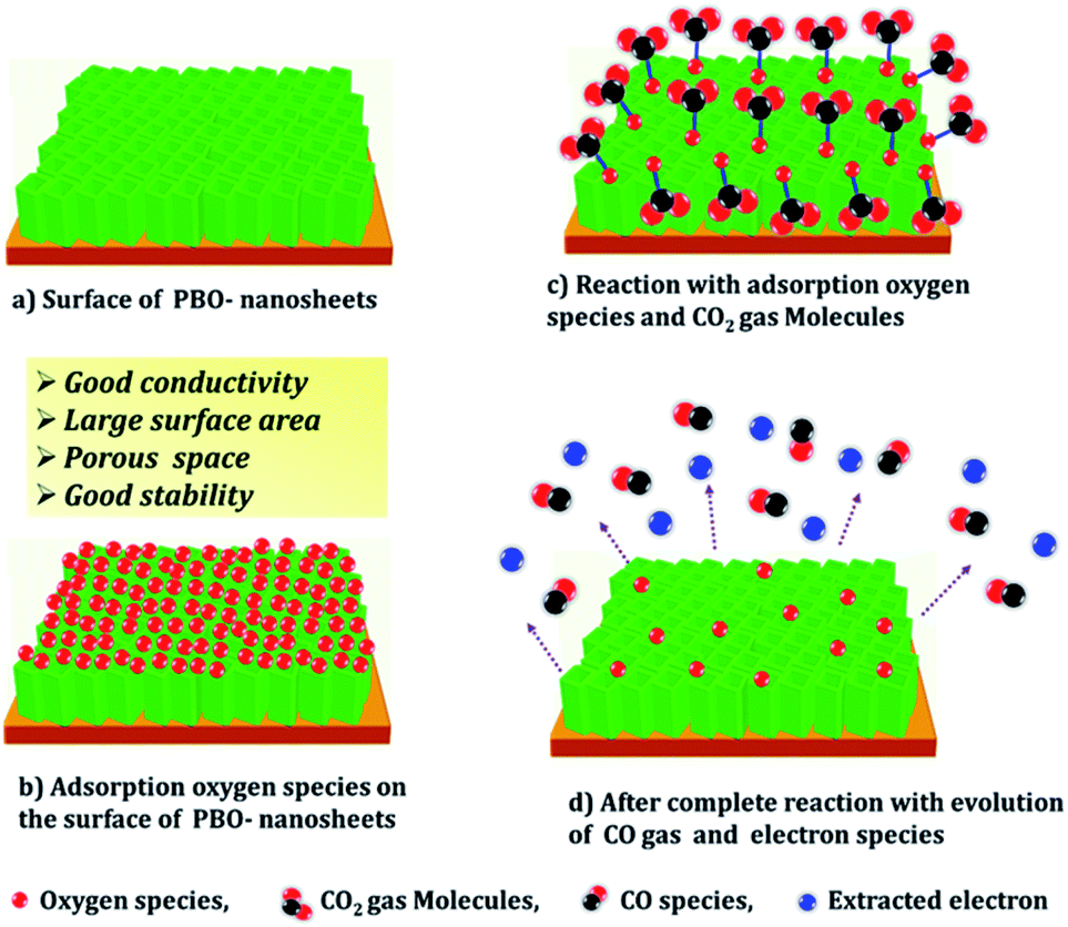
3.5 Gas-sensing mechanism
The semiconducting metal-oxide-based sensors gas-sensing mechanism, principally depends upon a variation in the electrical resistance of the sensing material which is mainly caused by the adsorption/desorption of the target gas molecules on the sensor surface upon the interaction of different target gases.61 In the present gas-sensing study, a sudden increase in the resistance values of the BO, PBO, EBO, and ABO nanosensors upon the collaboration of the CO2 gas was mainly accredited to the adsorption/desorption process of the CO2 molecules. Moreover, we explore the gas-sensing mechanism of the PBO-nanosheet CO2-gas sensor (ref. Fig. 7), and all the other nanosensors are shown in Fig. S7.† As the BO, PBO, EBO, and ABO nanosensors were exposed to air, the oxygen molecules from the air could be adsorbed on their surfaces by trapping electrons from its conduction band (Fig. 7a and b), thus ensuring the formation of an electron depletion layer with a slightly higher resistance.59 The adsorbed oxygen molecules are temperature dependent,62 i.e., O2 can accept one electron and form O2− below the temperature of 100 °C, O− at approximately 100–300 °C, and O2− at a temperature above 300 °C. In the present study, below the temperature of 100 °C, O2 could accept one electron from the BO, PBO, EBO, and ABO nanosensor surfaces (eqn (14) and (15)).| | |
O2 (ads) → O2 (ads)−
| (15) |
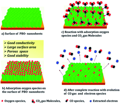 |
| | Fig. 7 (a–d) Different stages of gas sensing mechanism of the PBO nanosensor in air and CO2 gas. | |
The CO2-gas-sensing mechanism of the BO, PBO, EBO, and ABO nanosensors in the air can be clarified on the source of the reaction with the adsorbed oxygen species (Fig. 7b and S7†). Thus, the chemisorbed oxygen reasons electron depletion, thus creating a space-charge cover on the BO, PBO, EBO, and ABO nanosensor surfaces and ensuing in the creation of a Schottky surface barrier.63 When the CO2 gas is inserted into the compartment, the chemisorbed oxygen O2 (ads)− responds with the CO2 gas, which results in the evolution of CO gas and electron (e−) species (eqn (16), (17), Fig. 7c and d), and the response to the CO2 gas at room-temperature is evidenced as given below.14,18
| | |
Bi2O3 + O2 → (Bi2O3)O2−
| (16) |
| | |
(Bi2O3)O2− + CO2 (gas) → (Bi2O3)O− + CO(gas) + e−
| (17) |
With this reaction, many extracted electrons could be released to the BO, PBO, EBO, and ABO nanosensors surfaces, thus resulting in a Schottky-surface-barrier decrease with a thinner space-charge layer. Therefore, the electrical conductivity of the BO, PBO, EBO, and ABO nanosensor layers was increased at room-temperature. Moreover, the pores were regularly distributed over the BO, PBO, EBO, and ABO Bi2O3 nanosensors surfaces that could offer several channels to simplify the CO2 gas dispersal, thus more easily create an interaction of the CO2 gas with the inner Bi2O3 grains in the reduction reaction process and degassing equally during the recovery process as the porous surface delivers appropriate gas absorption surface sites; thereby, more gas molecules would be absorbed at a relatively low-temperatures, which reasons an improvement of the CO2-gas sensitivity (Fig. 7d). Consequently, the mesoporous BO, PBO, EBO, and ABO nanosensors played a vital role while obtaining fast response/recovery action.
3.6 Humidity-sensing activity
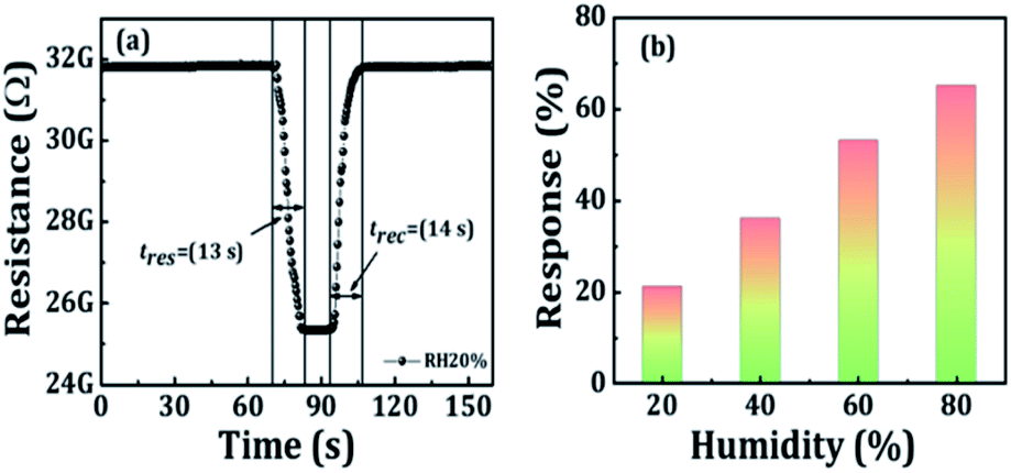
In addition, the sensor signals in dry air and humid air differ not only quantitatively but also qualitatively. The dry-air- and humid-air-sensing activities of the sensor were investigated using a two-electrode film system. The PBO sensing materials exhibited a high sensing performance as compared to those of BO, ABO, and EBO in CO2 gas. Therefore, only PBO sensing material was selected for the dry- and humid-air-sensing activities in dry air, even one hour of CO2 gas exposure was insufficient for reaching a steady response time, which is specifically noticeable after the stepwise rise in the CO2 gas concentration. The relative humidity (RH) conditions were realized through saturated salt solutions at room-temperature (27 °C). In the case of the PBO film sensor under 20% RH surroundings, the resistance reduced with the relative humidity, thus approving that the H2O molecules from the saturated salts represented as electron donors. H2O molecules adsorbed on the surface of the film sensor could modify the Fermi level close to the conduction band edge. Furthermore, the humidity-sensing mechanism was allied with the adsorption of H2O molecules on the surface of the sensor material.46,64
The humidity sensing activity of the PBO film sensor exhibited a 21% response for 20% RH at room-temperature (see Fig. 8a). The quick response/recovery time (13/14 s) was allocated to the quick desorption procedure of H2O molecules from the PBO sensor surface, thus resulting to the rapid adsorption/desorption of H2O molecules. The response of the Bi2O3 sensor device, which is limited by a heavy adsorption/desorption at room-temperature, was recognized to the thermodynamic progression of the H2O molecules taking place through adsorption, which was not satisfactory during the desorption as an outcome of the low absorption energy.65 Fig. 8b shows the enlarged response of the PBO sensor to humidity as the RH increased. Under humidity-sensing-activity conditions, the sensor response/recovery time was much smaller than the exposure times. Such an enhancement in the sensing performance under humid conditions is rather uncommon for a chemoresistive sensor. Naturally, semiconducting metal oxide sensors used for reducing gases suffer from cross-sensitivity to H2O vapor.4 The improved sensor signal in the case of CO2 in the presence of humidity highlighted the great prospective of the PBO sensors for applications further down the actual working circumstances.
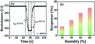 |
| | Fig. 8 Humidity-sensing properties of the PBO sensor; (a) variation of the resistance of PBO sensor with respect to 20% RH, (b) response of the PBO sensor with respect to various RH conditions. | |
4. Conclusion
In summary, a room-temperature, direct, and superfast chemical-bath deposition method has successfully been applied for synthesizing various morphologies (woollen globes, nanosheets, rose-flowers, and spongy-square plates) of Bi2O3 nanosensors on a glass substrate. These nanosensors are exploited as gas sensors where excellent sensing performances for CO2 gas at room-temperature are evidenced. The sensing response of the PBO nanosensor (179%) for CO2 gas at 100 ppm is higher than that of the BO (123%), EBO (158%), and ABO (132%) nanosensors structures. The response time/recovery time values of BO, PBO, EBO, and ABO nanosensors are respectively 151/28 s, 132/82 s, 77/82 s, and 89/32 s. These results emphasize the potential applications of room-temperature-synthesized Bi2O3 nanosensors for room-temperature operating CO2 gas sensors. The PBO nanosensor has endowed highest sensing performance as compared to those of the BO, ABO, and EBO nanosensors owing to a moderate diameter and uniform distribution of the nanosheets. Furthermore, the quick response/recovery time (13/14 s) of the humidity-sensing activity of the PBO film sensor with a 21% response for 20% RH at room-temperature (27 °C) is awesome for potential applications like in optoelectronic devices.
Conflicts of interest
There are no conflicts to declare.
Acknowledgements
This study was supported by the Global Frontier Program through the Global Frontier Hybrid Interface Materials of the National Research Foundation of Korea funded by the Ministry of Science, ICT & Future Planning (2013 M3A6B1078874) and National Core Research Centre grant 2015M3A6B1065262. The authors SFS and AME would like to extend their sincere appreciation to the Researchers supporting project number (RSP-2019/55), King Saud University, Riyadh, Saudi Arabia for funding this research.
Notes and references
- D. D. Lee and D. S. Lee, IEEE Sens. J., 2001, 1, 214–224 CAS.
- Y. Liu, J. Parisi, X. Sun and Y. Lei, J. Mater. Chem. A, 2014, 2, 9919–9943 RSC.
- L. Wang, T. Zhou, R. Zhang, Z. Lou, J. Deng and T. Zhang, Sens. Actuators, B, 2016, 227, 448–455 CrossRef CAS.
- I. Djerdj, A. Haensch, D. Koziej, S. Pokhrel, N. Barsan, U. Weimar and M. Niederberger, Chem. Mater., 2009, 21, 5375–5381 CrossRef CAS.
- A. Marsal, A. Cornet and J. R. Morante, Sens. Actuators, B, 2003, 94, 324–329 CrossRef CAS.
- R. B. Pedhekar and F. C. Raghuwanshi, International Journal of Engineering and Science Invention, 2017, 6, 20–28 Search PubMed.
- D. J. Wales, J. Grand, V. P. Ting, R. D. Burke, K. J. Edler, C. R. Bowen, S. Mintova and A. D. Burrows, Chem. Soc. Rev., 2015, 44, 4290–4321 RSC.
- G. F. Fine, L. M. Cavanagh, A. Afonja and R. Binions, Sensors, 2010, 10, 5469–5502 CrossRef CAS PubMed.
- N. B. Tanvir, O. Yurchenko, C. Wilbertz and G. Urban, J. Mater. Chem. A, 2016, 4, 5294–5302 RSC.
- C. Willa, A. Schmid, D. Briand, J. Yuan and D. Koziej, ACS Appl. Mater. Interfaces, 2017, 9, 25553–25558 CrossRef CAS PubMed.
- M. I. Baraton, Sens. Actuators, B, 1996, 31, 33–38 CrossRef CAS.
- M. Holzinger, J. Maier and W. Sitte, Solid State Ionics, 1997, 94, 217–225 CrossRef CAS.
- J. Bobacka, A. Ivaska and A. Lewenstam, Chem. Rev., 2008, 108, 329–351 CrossRef CAS PubMed.
- S. S. Bhande, R. S. Mane, A. V. Ghule and S. H. Han, Scr. Mater., 2011, 65, 1081–1084 CrossRef CAS.
- H. Zhang, S. Wang, Y. Wang, J. Yang, X. Gao and L. Wang, Phys. Chem. Chem. Phys., 2014, 16, 10830 RSC.
- M. Fleischer, Meas. Sci. Technol., 2008, 19, 42001 CrossRef.
- H. S. Hong, L. T. Dai, T. Trung and H. N. Van, Talanta, 2012, 88, 152–159 CrossRef PubMed.
- M. Ahila, J. Dhanalakshmi, J. C. Selvakumari and D. P. Padiyan, Mater. Res. Express, 2016, 3, 105025 CrossRef.
- K. Fan, H. Qin, L. Wang, L. Ju and J. Hu, Sens. Actuators, B, 2013, 177, 265–269 CrossRef CAS.
- D. Gibson and C. MacGregor, Sensors, 2013, 13, 7079–7103 CrossRef CAS PubMed.
- F. C. Bancolo, G. N. C. Santos and R. V. Quiroga, Int. J. Sci. Eng. Res., 2012, 3, 1–6 Search PubMed.
- O. Hirsch, K. O. Kvashnina, L. Luo, M. J. Suess, P. Glatzel and D. Koziej, Proc. Natl. Acad. Sci. U. S. A., 2015, 112, 15803–15808 CrossRef CAS PubMed.
- A. Golev, M. Scott, P. D. Erskine, S. H. Ali and G. R. Ballantyne, Resour. Pol., 2014, 41, 52–59 CrossRef.
- F. R. Juang, IEEE Sens. J., 2019, 19, 4381–4385 CAS.
- C. D. Lokhande, P. M. Gondkar, R. S. Mane, V. R. Shinde and S. H. Han, J. Alloys Compd., 2009, 475, 304–311 CrossRef CAS.
- I. I. Oprea, H. Hesse and K. Betzler, Opt. Mater., 2004, 26, 235–237 CrossRef CAS.
- T. A. Hanna, Coord. Chem. Rev., 2004, 248, 429–440 CrossRef CAS.
- A. M. Azad, S. Larose and S. A. Akbar, J. Mater. Sci., 1994, 29, 4135–4151 CrossRef CAS.
-
(a) N. M. Shinde, Q. X. Xia, J. M. Yun, S. Singh, R. S. Mane and K. H. Kim, Dalton Trans., 2017, 46, 6601–6611 RSC;
(b) L. Wang, T. Zhou, R. Zhang, Z. Lou, J. Deng and T. Zhang, Sens. Actuators, B, 2016, 227, 448–455 CrossRef CAS;
(c) P. S. Gaikar, S. T. Navale, V. V. Jadhav, P. V. Shinde, D. P. Dubal, P. R. Arjunwadkar, F. J. Stadler, M. Naushad, A. A. Ghfar and R. S. Mane, Electrochim. Acta, 2017, 253, 151–162 CrossRef CAS.
- H. Weidong, Q. Wei, W. Xiaohong, D. Xianbo, C. Long and J. Zhaohua, Thin Solid Films, 2007, 515, 5362–5365 CrossRef.
- Z. N. Adamian, H. V. Abovian and V. M. Aroutiounian, Sens. Actuators, B, 1996, 35, 241–243 CrossRef CAS.
- E. T. Salim, Y. Al-Douri, M. S. Al Wazny and M. A. Fakhri, Sol. Energy, 2014, 107, 523–529 CrossRef CAS.
- L. Li, Y. W. Yang, G. H. Li and L. D. Zhang, Small, 2006, 2, 548–553 CrossRef PubMed.
- L. Kumari, J. H. Lin and Y. R. Ma, Nanotechnol, 2007, 18, 295605–295612 CrossRef.
- L. Kumari, J. H. Lin and Y. R. Ma, J. Phys.: Condens. Matter, 2007, 19, 406204–406215 CrossRef PubMed.
- H. Nguyen and S. A. El-Safty, J. Phys. Chem. C, 2011, 115, 8466–8474 CrossRef CAS.
- T. P. Gujar, V. R. Shinde, C. D. Lokhande and S. H. Han, Mater. Sci. Eng., B, 2006, 133, 177–180 CrossRef CAS.
- P. V. Shinde, B. G. Ghule, N. M. Shinde, Q. X. Xia, S. F. Shaikh, A. V. Sarode, R. S. Mane and K. H. Kim, New J. Chem., 2018, 42, 12530–12538 RSC.
- L. L. Wang, Z. Lou, T. Fei and T. Zhang, Sens. Actuators, B, 2012, 161, 178–183 CrossRef CAS.
- Y. Q. Jiang, C. X. He, R. Sun, Z. X. Xie and L. S. Zheng, Mater. Chem. Phys., 2012, 136, 698–704 CrossRef CAS.
- H. G. Zhang, Q. S. Zhu, Y. Zhang, Y. Wang, L. Zhao and B. Yu, Adv. Funct. Mater., 2007, 17, 2766–2771 CrossRef CAS.
- J. H. Lee, Sens. Actuators, B, 2009, 140, 319–336 CrossRef CAS.
- Y. S. Wang, S. R. Wang, H. X. Zhang, X. L. Gao, J. D. Yang and L. W. Wang, J. Mater. Chem. A, 2014, 2, 7935 RSC.
- K. Nam, H. G. Kim, H. Choi, H. Park, J. S. Kang, Y. E. Sung, H. C. Lee and H. Choe, J. Electron. Mater., 2017, 6, 3748–3756 CrossRef.
- N. M. Shinde, Q. X. Xia, J. M. Yun, R. S. Mane and K. H. Kim, ACS Appl. Mater. Interfaces, 2018, 10, 11037–11047 CrossRef CAS PubMed.
- P. V. Shinde, B. G. Ghule, S. F. Shaikh, N. M. Shinde, S. S. Sangale, V. V. Jadhav, S. Y. Yoon, K. H. Kim and R. S. Mane, J. Alloys Compd., 2019, 802, 244–251 CrossRef CAS.
- S. T. Navale, C. Liu, P. S. Gaikar, V. B. Patil, R. U. R. Sagar, B. Du, R. S. Mane and F. J. Stadler, Sens. Actuators, B, 2017, 245, 524–532 CrossRef CAS.
- H. Deng, L. Lin, M. Ji, S. Zhang, M. Yang and Q. Fu, Prog. Polym. Sci., 2014, 39, 627–655 CrossRef CAS.
- Y. Tian, G. Hua, W. Xu, N. Li, M. Fang and L. Zhang, J. Alloys Compd., 2011, 509, 724–727 CrossRef CAS.
- H. Jiang, T. Zhao, C. Li and J. Ma, J. Mater. Chem., 2011, 21, 3818–3823 RSC.
- J. Xiao and S. Yang, RSC Adv., 2011, 1, 588–595 RSC.
- J. Chen, X. Xia, J. Tu, Q. Xiong, Y. Yu, X. Wang and C. Gu, J. Mater. Chem., 2012, 22, 15056–15061 RSC.
- Y. Qiu, D. Liu, J. Yang and S. Yang, Adv. Mater., 2006, 18, 2604–2608 CrossRef CAS.
- C. Chang, H. C. Yang, N. Gao and S. Y. Lu, J. Alloys Compd., 2018, 738, 138–144 CrossRef CAS.
- H. Guan, X. Zhang and Y. Xie, J. Phys. Chem. C, 2014, 118, 27170–27174 CrossRef CAS.
- W. Zuo, W. Zhu, D. Zhao, Y. Sun, Y. Li, J. Liu and X. W. Lou, Energy Environ. Sci., 2016, 9, 2881–2891 RSC.
- Z. Zhang, R. Zou, G. Song, L. Yu, Z. Chen and J. Hu, J. Mater. Chem., 2011, 21, 17360 RSC.
- H. Na, X. Zhang, Z. Deng, Y. Xu, L. Huo and S. Gao, ACS Appl. Mater. Interfaces, 2019, 11, 11627–11635 CrossRef CAS PubMed.
- S. D. Waghmare, D. V. Shinde, M. K. Zate, R. Konda, R. S. Mane and S. H. Han, Scr. Mater., 2013, 68, 735–738 CrossRef CAS.
- X. Zhou, B. Wang, H. Sun, C. Wang, P. Sun, X. Li, X. Hu and G. Lu, Nanoscale, 2016, 8, 5446–5453 RSC.
- F. Song, H. Su, J. Han, J. Xu and D. Zhang, Sens. Actuators, B, 2010, 145, 39–45 CrossRef CAS.
- P. Shankar and J. Bosco, Sci. Lett. J., 2015, 4, 126 Search PubMed.
- A. Marsal, G. Dezanneau, A. Cornet and J. R. Morante, Sens. Actuators, B, 2003, 95, 266–270 CrossRef CAS.
- A. S. Pawbake, R. G. Waykar, D. J. Late and S. R. Jadkar, ACS Appl. Mater. Interfaces, 2016, 8, 3359–3365 CrossRef CAS PubMed.
- L. D. Bharatula, M. B. Erande, I. S. Mulla, C. S. Rout and D. J. Late, RSC Adv., 2016, 6, 105421–105427 RSC.
Footnote |
| † Electronic supplementary information (ESI) available: Modern techniques used for analysis, the repeatability of transient versus time, response versus time (at 100 ppm), and stability measurements of the BO, PBO, EBO, and ABO film sensors, survey XPS, and enlarged XPS spectra of Bi4f before and after the CO2-gas sensing, etc. See DOI: 10.1039/d0ra00801j |
|
| This journal is © The Royal Society of Chemistry 2020 |
Click here to see how this site uses Cookies. View our privacy policy here. 
 Open Access Article
 This Open Access Article is licensed under a Creative Commons Attribution-Non Commercial 3.0 Unported Licence
 a,
Nanasaheb M. Shinde
a,
Nanasaheb M. Shinde