
 Open Access Article
 This Open Access Article is licensed under a Creative Commons Attribution-Non Commercial 3.0 Unported Licence
Conversion of WO3 thin films into self-crosslinked nanorods for large-scale ultraviolet detection†
Youngho Kim‡
ab,
Sang Hoon Lee‡c,
Seyoung Jeongb,
Bum Jun Kimd,
Jae-Young Choi *cd and
Hak Ki Yu*ab
*cd and
Hak Ki Yu*ab
aDepartment of Materials Science and Engineering, Department of Energy Systems Research, Ajou University, Suwon, 16499, Republic of Korea. E-mail: hakkiyu@ajou.ac.kr
bDepartment of Materials Science and Engineering, Ajou University, Suwon 16499, South Korea
cSchool of Advanced Materials Science & Engineering, Sungkyunkwan University, Suwon, 16419, Republic of Korea. E-mail: jy.choi@skku.edu
dSKKU Advanced Institute of Nanotechnology (SAINT), Sungkyunkwan University, Suwon, 16419, Republic of Korea
First published on 6th April 2020
Abstract
We heat-treated an amorphous large-area WO3 thin film to synthesize high-density, high-quality WO3 nanorods. The WO3 nanostructures were effective, especially in reducing gas (hydrogen and helium) atmospheres. By electron microscopy analysis, we confirmed that the thermodynamic energy for forming oxygen vacancies in the [020] direction was low. We could apply self-crosslinked WO3 nanostructures to practical sensor device fabrication by simply placing the electrodes without complex processes such as transfer and e-beam lithography. It was used for the production of a UV detector, which reacted very fast (∼0.316 s) and was very sensitive to the actual UV-C (261 nm) wavelength. Also, plasmon-based light absorption through the Ag nanoparticle coating resulted in more than 350-fold improvement in the on/off process during UV-C irradiation.
Introduction
Among the solar radiations reaching the earth's surface, the ultraviolet (UV) portion has a lot of direct and indirect effects on human life. A proper amount of UV radiation has a positive impact such as sterilization, synthesis of vitamin D, and promotion of plant growth. However, overexposure to UV radiation causes aging of organisms and skin cancer.1–3 In recent years, there has been an increasing concern about the excessive exposure to UV rays due to the destruction of the ozone layer by global warming and therefore, research on a device capable of detecting UV rays is becoming more important.4–7 In general, the most critical factor for detecting UV light is a semiconductor material having a bandgap. Various materials have been studied, ranging from Si, which is used as a conventional electronic device, to InP and GaN, which are optical semiconductors. However, to fabricate a more sensitive detector at the wavelength of the UV bandedge (UV-A: 3.1 eV, UV-B: 3.9 eV, and UV-C: 4.4 eV), oxide materials with large bandgaps are being studied.8–17Oxides are of many kinds and have atmospheric stability; above all, their bandgap (>3.1 eV) has a significant advantage because oxygen can strongly attract the electrons of metal ions. However, since the mobility of electrons is low, the sensitivity of UV detection may be lowered. In this study, we fabricated a UV detector using WO3, which has a direct bandgap of >3.3 eV, and its electron mobility is excellent among oxides with regard to n-type characteristics.18–23 Nanorod or thin-film structures have been used in manufacturing UV detectors using WO3 materials. Nanorods can be expected to have high sensitivity due to their excellent crystallinity, but they have the disadvantages of high process cost (e-beam lithography, etc.) and reproducibility for large-area synthesis and single nanodevice fabrication.24,25 On the other hand, in the case of polycrystalline thin-film fabrication, although there is a reduction in the sensitivity of the device due to the reduction in electron mobility, there is an advantage that a large-area device is easily manufactured.26–30
In this study, to obtain only the advantages of these methods, a large-area WO3 thin film was deposited on a specific substrate and then heat-treated to synthesize high-density nanorods using stresses resulting from the thermal expansion coefficient differences of the substrate. The self-connecting method was used to manufacture a UV detector easily. In this way, the length and density of the nanorods can be controlled by adjusting the temperature and time of the heat treatment. It is expected that this method can be easily applied to large-area mass production because the device can be easily manufactured by using only a bulk-paste electrode when manufacturing a UV detector.
Experimental
Growth of self-crosslinked WO3 nanorods
We cleaned each substrate (Si (100) covered with a thermal oxide of 200 nm (Namkang Hi-Tech, SSP), c-plane Al2O3 (Crystal Bank, SSP)) sequentially using acetone, isopropyl alcohol, and deionized water. The WO3 thin film (10 nm thickness) was deposited on the substrate using an e-beam evaporator (the base pressure was ∼10−6 torr) using the source of the WO3 pellet (ITASO, EWA0LT0017, 99.95% purity). Furthermore, we performed heat treatment in a tube furnace to convert the grown WO3 film into nanostructures. The base pressure of the tube furnace was ∼10−3 torr, and we performed the heat treatment at 700 °C (heating rate was 17.5 °C min−1) with a gas flow of 40 sccm depending on the heat treatment atmosphere (H2, He, and O2). We deposited a thin layer of Ag on the WO3 nanostructure using a thermal evaporator to coat the Ag nanoparticles and further performed heat treatment at 300 °C for 5 minutes. The in situ process for Ag nanoparticles was conducted in one chamber.Analysis
We performed X-ray diffraction (XRD; Rigaku, D/max-2500V/PC, monochromated Cu Kα1 radiation; scan rate = 3° min−1, Japan) to identify the crystal structures of the prepared samples. We investigated the surface morphology of the samples using scanning electron microscopy (SEM; JEOL, JSM-6700F, accelerating voltage = 5 kV, Japan) and high resolution-transmission electron microscopy (HR-TEM; JEOL, JEM-2100, accelerating voltage = 200 kV, Japan). We obtained the current–voltage (I–V) curves and time-dependent responses of the fabricated UV detectors using a probe station (MSTECH, MST5000); we used a single wavelength (254 nm/365 nm) UV lamp (VILBER, VL-215 LC) as the UV source. The performance of the UV detector was evaluated in vacuum.Results and discussion
First, when the substrate with the WO3 thin film was annealed, compressive stress was generated in the WO3 thin film due to a gradient of the thermal expansion coefficients between the WO3 film and the substrate (Si: 2.4 × 10⁻⁶, Al2O3: 8.0 × 10⁻⁶, and WO3: 12 × 10−6 K−1).31,32 This compressive stress induced agglomeration of WO3, providing a seed for the growth of nanostructures. Also, when annealing was carried out in an atmosphere of hydrogen or helium, WO3 was reduced by generating oxygen vacancies. The oxygen vacancies in WO3 are known to be more preferred for the (200) plane.33 The oxygen vacancies increase during annealing in a reducing atmosphere, and the increased defects are provided with sufficient activation energy to diffuse into a stable plane. Therefore, the oxygen vacancies were arranged in the 〈020〉 direction to form planar defects (parallel to the (200) plane), and the seeds could grow into nanorods along the arrangement. The WO3 nanorods grown by this mechanism were formed in random directions on wafers to realize a self-connecting structure. This process is illustrated in Fig. 1.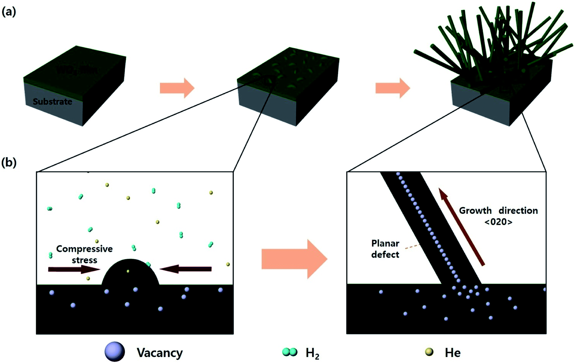 | ||
| Fig. 1 The schematic illustration of growth mechanism of WO3 nanorods during annealing in a reducing atmosphere: (a) the growing steps for WO3 nanorods, (b) the detail of each step in the reaction. | ||
Fig. 2a shows the SEM images of the WO3 film after annealing at 700 °C in various gas atmospheres. Immediately after deposition, it was flat without significant roughness. Annealing without the injection gas appeared to slightly increase the roughness. This is expected to cause the agglomeration of the WO3 thin film at a high temperature. After annealing in an H2 atmosphere, the nanorods grew according to the mechanism described previously (Fig. 1). After annealing in an O2 atmosphere, the material was formed with a flake shape instead of a nanorod. The SEM images in Fig. 2b indicate comparative substrates of Si and Al2O3 after annealing in an He atmosphere (a similar effect as that in the H2 atmosphere as a reducing environment). Although the WO3 thin film generated compressive stress on the Al2O3 substrate due to the gradient of the thermal expansion coefficient, the gradient was relatively smaller than that for the WO3 thin film on the Si substrate, resulting in low density of nanorods. As can be seen from the XRD patterns shown in Fig. 2c, the WO3 thin film in the as-deposited state is amorphous. However, it can be seen that crystals appear after heat treatment, and the crystal orientations differ depending on the heat treatment atmosphere. The (200) plane is preferred in an oxidizing atmosphere because for WO3, it is known that the (200) plane is active for oxidation reactions.34 In contrast, the (020) plane is preferred in a reducing atmosphere such as He. This is because as mentioned above, the WO3 nanorods growing in a reducing atmosphere tend to have a growth direction in the family direction of the [020].
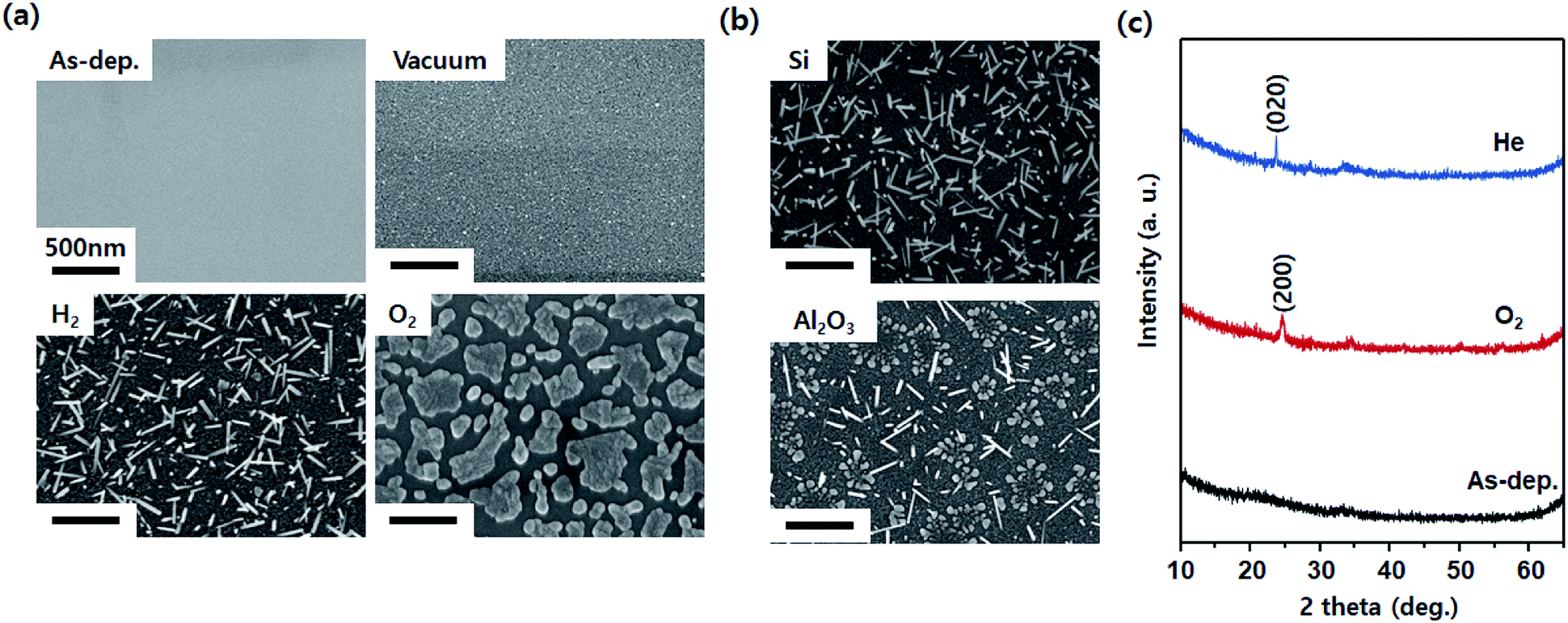 | ||
| Fig. 2 SEM images of WO3 after annealing at 700 °C with respect to (a) gas atmosphere and (b) substrate type. (c) XRD pattern of WO3 annealed in oxidizing (O2 gas) and reducing (He gas) atmospheres. | ||
As shown in the ESI S1,† the thickness of amorphous WO3 and the heat treatment temperature were adjusted. When the heat treatment was conducted at 700 °C, high thickness was confirmed, indicating that the compressive stress was not applied on the surface of the thin film. When the thin film of 50 nm thickness was heat-treated at other temperatures, it was confirmed that the diameter of the nanorod increased at a relatively higher temperature. However, it was determined that the higher the heat treatment temperature, the more difficult it was to apply the process in actual industries. Therefore, the optimal growth conditions were selected: thickness of 10 nm and annealing temperature of 700 °C.
The TEM image shown in Fig. 3 displays the cross-section of the WO3 film on SiO2/Si, which was annealed for 3 minutes in an He atmosphere. It indicates partial agglomeration and crystallinity. Additionally, the lattice spacing of the partially crystalline phase has a (020) interplanar distance. Furthermore, it can be seen that the other parts still remain amorphous. In other words, as the amorphous thin film is agglomerated by compressive stress and is consumed as crystalline nanorods, it can be seen that the growth in the 〈020〉 direction begins. The WO3 nanorods are known to grow along the direction in which defects are arranged. Moreover, in this case, we understand that the diffraction patterns stretch perpendicularly to the growth direction.33 This is because the interplanar distance of the plane parallel to planar defects can be slightly changed. Fig. 4 displays the TEM images of a WO3 single nanorod. As can be seen from the HR-TEM images and SAED patterns in Fig. 4a, the grown WO3 nanorod has excellent crystallinity, which will be an advantage for future sensor devices. Additionally, the Fourier filtering image shows that the interplanar distance is similar to the literature value for the (020) plane. The terminating surface of the WO3 nanorod is the {200} plane, which has the lowest surface energy. In Fig. 4b, it can be seen that planar misfit defects occur in the 〈020〉 direction of the WO3 nanorods. This supports the earlier claim about the defect-based nanorod growth.
 | ||
| Fig. 3 TEM images and SAED patterns of cross-sectional WO3 thin film on SiO2/Si after annealing for 3 min in He atmosphere. | ||
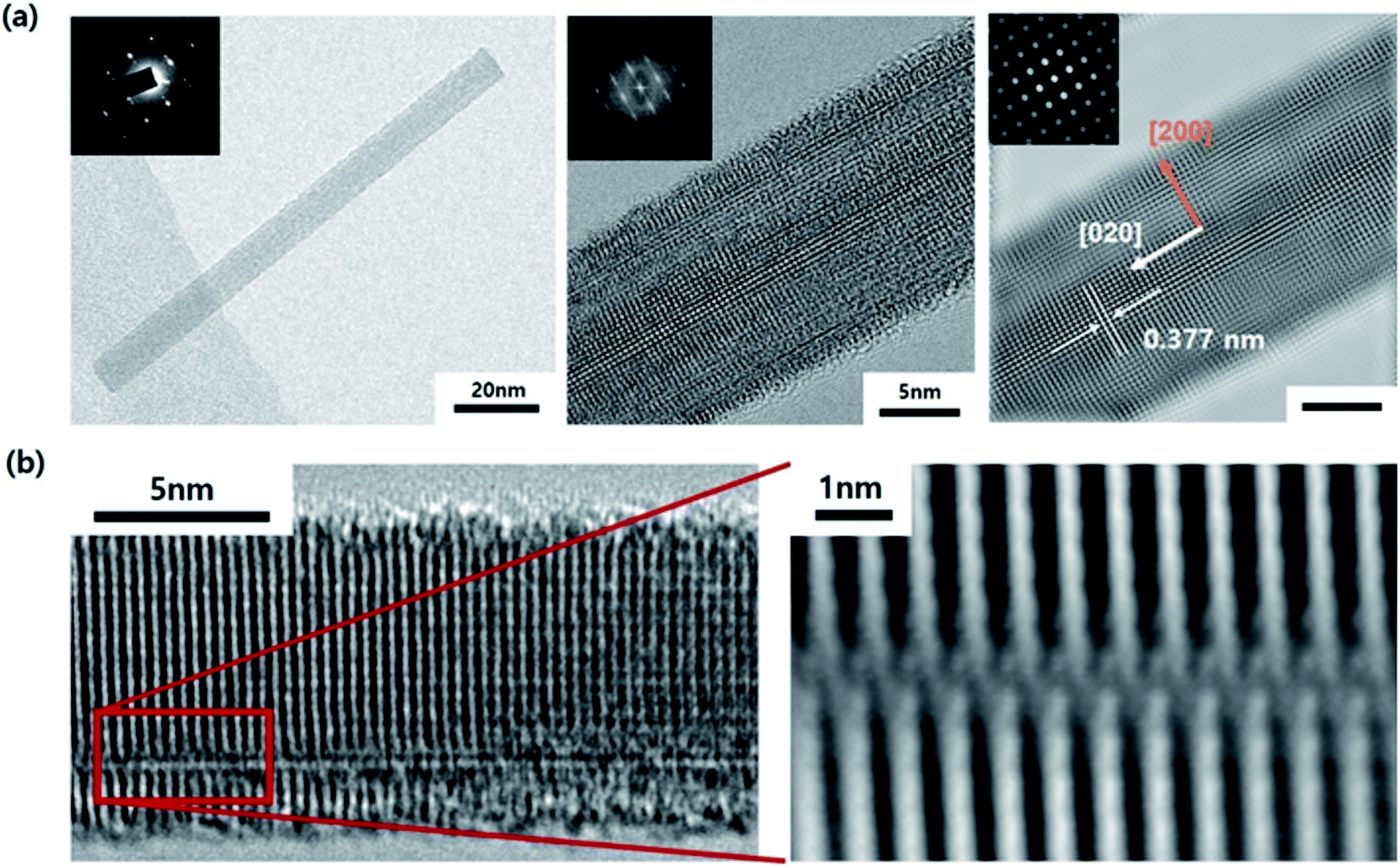 | ||
| Fig. 4 (a) TEM images and SAED patterns of a WO3 single nanorod. (b) HR-TEM images of planar misfit defects in a WO3 nanorod. | ||
Even if we grew the nanorods via annealing in both H2 and He atmospheres, the residue of the WO3 thin film seemed to remain (Fig. 2a and b). Through successive annealing, the growth of longer nanorods was possible by the consumption of the residual WO3 film as the source material. The changes in the length and density of the WO3 nanorods with the annealing time can be seen in the SEM image in Fig. 5. As shown in Fig. 5a, after 5 minutes of annealing, only fine dots are formed. As the annealing time increased to 20 minutes, very short nanorods began to form. After that, as the annealing time further increased, the density and length of the nanorods increased. Finally, when the annealing time reached 8 hours, the WO3 nanorods exhibited a self-crosslinking system. Thus, this system can be a UV sensor without lithographic patterning. After 4 hours of annealing time, voids appeared without nanorods or residues, which were regarded to be caused by the depletion of the WO3 thin film. The cross-sectional SEM image in Fig. 5b shows that the nanorods grow not only horizontally, but also vertically. This structure is also expected to be beneficial for the absorption of UV light. Additionally, Ag nanoparticles were decorated on the WO3 nanorods to increase the UV light absorption due to the surface plasmon phenomenon. This can be seen in the last SEM image in Fig. 5a.
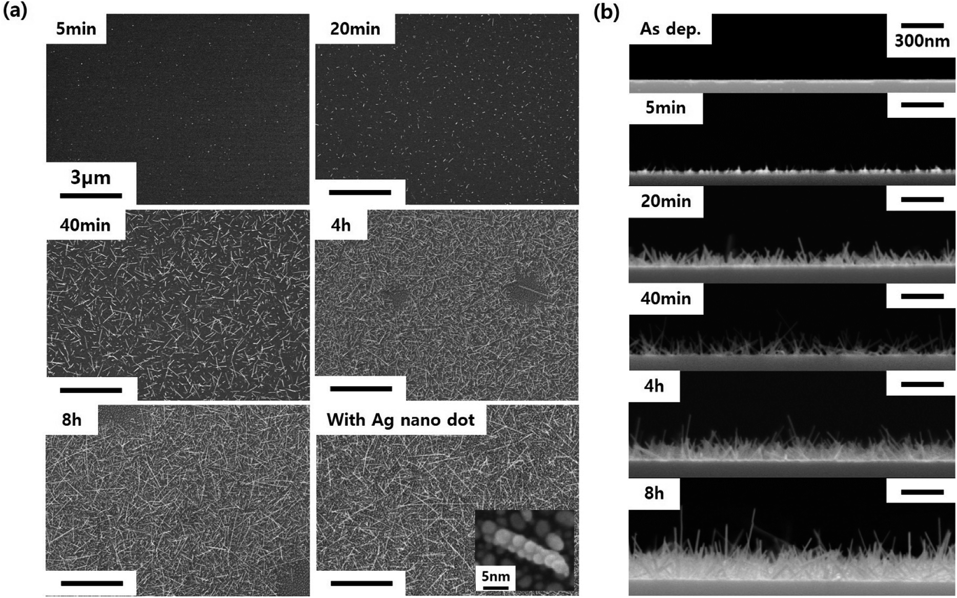 | ||
| Fig. 5 SEM images of WO3 nanorods depending on the annealing time and Ag decoration; (a) top view and (b) cross-sectional view. | ||
As illustrated in Fig. 6a, we carried out performance measurements as a UV sensor using the two electrodes of Ag paste on the self-crosslinked WO3 sample annealed for 8 hours.35 This method involves a simple mechanism. The carriers can be generated by inter-band transitions due to the absorption of UV rays. The generated carriers can be transported between each WO3 nanorod. Finally, it can overcome the barrier of the band structure between the WO3 nanorod and the electrode by sufficient voltage. Since WO3 is an n-type semiconductor, other metals such as Ti and Al are more suitable as electrodes. Thus, the Schottky barrier between WO3 and Ag can be relatively high. Nevertheless, the reason for using Ag paste is that the method of making an Ag electrode is not only diverse but also economical. Therefore, it is favourable for process development for industrial applications. Fig. 6c and d show the results of the response function regarding irradiation using 261 nm UV (UV-C region) light. In both cases, with or without Ag nanodots, the reaction rate was 316 ms, and the currents generated during UV irradiation were 9.42 × 10⁻¹² A and 3.33 × 10⁻⁹ A. Responding to the UV radiation despite the absence of Ag decoration means that the self-crosslinked structure is realized. When the Ag nanoparticles were coated, the photocurrent by UV irradiation increased by about 350-fold. This suggests that Ag increases the absorption of UV light through the plasmon effect. The absorption of light or electromagnetic waves by the plasmon effect and its application are well known.36 From the ESI S2† displaying the UV detection performance of the amorphous thin film, comparing the nanorods, we infer that the amorphous thin film has a limitation in the response time and recovery. This late response time and slow recovery make it impossible to measure in real time during UV sensing. This difference in performances is expected to be caused by the crystallinity of each material. When the WO3 nanorods are irradiated by 365 nm UV (UV-A region) light, there is no response (ESI S3†). This means that the self-crosslinked WO3 nanostructure synthesized through this experiment can be well applied to sensors that selectively react to UV-C. As ozone depletion progresses, the amount of UV rays reaching the Earth's surface can increase. Among them, UV-C has relatively high energy. Even small amounts of UV-C can cause various problems (e.g., the destruction or degradation of devices, damage to the skin, etc.). Therefore, the selective detecting technology of UV-C will be needed in the future.
 | ||
| Fig. 6 (a) The schematic illustration of performance measurement of self-crosslinked WO3 nanorods as UV detector. (b) The real photograph of the UV detector. The photocurrent response of UV-C ray (216 nm) irradiation of self-crosslinked WO3 (c) without Ag nanoparticles and (d) with Ag nanoparticles. | ||
Conclusions
In conclusion, when the amorphous WO3 thin film was deposited and subjected to heat treatment, nanostructures started to form on the surface due to the difference in thermal expansion coefficients with respect to the substrate. At this time, when the heat treatment atmosphere was a reducing gas such as hydrogen or helium, the formed oxygen vacancies were arranged in the thermodynamically stable WO3 [020] direction, resulting in a specific growth direction of the WO3 nanorods. We can utilize this self-crosslinked high-density WO3 structure for practical device fabrication by simply placing electrodes without the transfer and e-beam lithographic processes required to fabricate unit nanorod devices. When we applied the WO3 nanostructures to a UV detection device, the UV-detection rate was highly sensitive (∼0.316 s) to the wavelength of the UV-C (261 nm) region, and UV detection was effectively performed. Additionally, it was confirmed that the on/off ratio increased significantly (more than 350 times) on increasing UV absorption through the Ag nanoparticle coating. We expect that the large-scale self-cross-linked WO3 nanostructures and UV-detector devices developed through this study will be widely used in the future for manufacturing various unit sensor devices and nanostructure fabrication.Conflicts of interest
There are no conflicts to declare.Acknowledgements
This research was supported by the Basic Science Research Program through the National Research Foundation of Korea (NRF), funded by the Ministry of Science and ICT (NRF-2019R1A2C1006972, NRF-2020R1A2C2010984).Notes and references
- A. J. Fornace, K. W. Kohn and H. E. Kann, Proc. Natl. Acad. Sci. U. S. A., 1976, 73, 39–43 CrossRef CAS PubMed.
- A. Scobodova, J. Psotova and D. Walerova, Biomed. Pap. Med. Fac. Palacky Univ. Olomouc Czech Repub., 2003, 147, 137–145 CrossRef.
- R. P. Sinha and D. P. Hader, Photochem. Photobiol. Sci., 2002, 1, 225–236 RSC.
- A. F. Bais, R. L. Mckenzie, G. Bernhard, P. J. Aucamp, M. Ilyas, S. Madronich and K. Tourpali, Photochem. Photobiol. Sci., 2015, 14, 19–52 RSC.
- R. M. Lucas, M. Norval, R. E. Neale, A. R. Young, F. R. Gruijl, Y. Takizawa and J. C. Van der Leun, Photochem. Photobiol. Sci., 2015, 14, 53–87 RSC.
- C. E. Williamson, P. J. Neale, S. Hylander, K. C. Rose, F. L. Figueroa, S. A. Robinson, D. P. Häder, S. Å Wängberg and R. C. Worrest, Photochem. Photobiol. Sci., 2019, 18, 717–746 RSC.
- K. Huang, Q. Zhang, F. Yang and D. He, Nano Res., 2010, 3, 281–287 CrossRef CAS.
- A. Ate and Z. Tang, Int. J. Optoelectron. Eng., 2014, 4, 6–10 Search PubMed.
- H. Chong, G. Wei, H. Hou, H. Yang, M. Shang, F. Gao, W. Yang and G. Shen, Nano Res., 2015, 8, 2822–2832 CrossRef CAS.
- W. Tian, H. Lu and L. Li, Nano Res., 2015, 8, 382–405 CrossRef CAS.
- J. Dai, W. Gao, B. Liu, X. Cao, T. Tao, Z. Xie, H. Zhao, D. Chen, H. Ping and R. Zhang, Appl. Surf. Sci., 2016, 364, 886–891 CrossRef CAS.
- X. Z. Liu, P. Guo, T. Sheng, L. X. Qian, W. L. Zhang and Y. R. Li, Opt. Mater., 2016, 51, 203–207 CrossRef CAS.
- M. Aghaeipour, N. Anttu, G. Nylund, L. Samuelson, S. Lehmann and M. E. Pistol, Opt. Express, 2014, 22, 29204–29212 CrossRef PubMed.
- D. Shao, M. Yu, J. Lian and S. Sawyer, Nanotechnology, 2013, 24, 295701 CrossRef PubMed.
- X. Fang, Y. Bando, M. Liao, T. Zhai, U. K. Gautam, L. Li, Y. Koide and D. Golberg, Adv. Funct. Mater., 2010, 20, 500–508 CrossRef CAS.
- S. J. Pearton, W. T. Lim, J. S. Wright, L. C. Tien, H. S. Kim, D. P. Norton, H. T. Wang, B. S. Kang, F. Ren, J. Jun, J. Lin and A. Osinsky, J. Electron. Mater., 2008, 37, 1426–1432 CrossRef CAS.
- L. Ravikiran, K. Radhakrishnan, N. Dharmarasu, M. Agrawal, Z. Wang, A. Bruno, C. Soci, T. Lihuang and K. S. Ang, IEEE Sens. J., 2016, 17, 72–77 Search PubMed.
- W. Cheng and M. Niederberger, Langmuir, 2016, 32, 2474–2481 CrossRef CAS PubMed.
- J. Liu, M. Zhong, J. Li, A. Pan and X. Zhu, Mater. Lett., 2015, 148, 184–187 CrossRef CAS.
- B. Cook, Q. Liu, J. Butler, K. Smith, S. Karen, D. Ewing, M. Casper, A. Stramel, A. Elliot and J. Wu, ACS Appl. Mater. Interfaces, 2018, 10, 873–879 CrossRef CAS PubMed.
- Z. He, Q. Liu, H. Hou, F. Gao, B. Tang and W. Yang, ACS Appl. Mater. Interfaces, 2015, 7, 10878–10885 CrossRef CAS PubMed.
- Z. Qi, J. Cao, L. Ding and J. Wang, Appl. Phys. Lett., 2015, 106, 053304 CrossRef.
- L. Li, Y. Zhang, X. Fang, T. Zhai, M. Liao, X. Sun, Y. Koide, Y. Bando and D. Golberg, J. Mater. Chem., 2011, 21, 6525 RSC.
- D. Shao, M. Yu, J. Lian and S. Sawyer, Opt. Mater., 2014, 36, 1002–1005 CrossRef CAS.
- Q. Yi, C. Hu, R. Yang, H. Liu, B. Wan and Y. Zhang, J. Alloys Compd., 2011, 509, L255–L261 CrossRef CAS.
- J. Malm, T. Sajavaara and M. Karppinen, Chem. Vap. Depos., 2012, 18, 245–248 CrossRef CAS.
- Z. Hai, M. K. Akbari, C. Xue, H. Xu, S. Depuydt and S. Zhuiykov, Sens. Actuators, B, 2017, 245, 954–962 CrossRef CAS.
- Z. Hai, M. K. Akbari, C. Xue, H. Xu, L. Hyde and S. Zhuiykov, Appl. Surf. Sci., 2017, 405, 169–177 CrossRef CAS.
- H. Na, Y. Eun, M. O. Kim, J. Choi and J. Kim, Sci. Rep., 2015, 5, 18265 CrossRef CAS PubMed.
- P. V. K. Yadav, Y. A. K. Reddy, B. Ajitha and V. R. M. Reddy, J. Alloys Compd., 2020, 816, 152565 CrossRef CAS.
- Y. A. K Reddy, B. Ajitha, A. Sreedhar and E. Varrla, Appl. Surf. Sci., 2019, 494, 575–582 CrossRef.
- R. R. Reeber and K. Wang, Mater. Res. Soc. Symp. Proc., 2000, 622, T6.35.1 CrossRef.
- J. Zhou, Y. Ding, S. Z. Deng, L. Gong, N. S. Xu and Z. L. Wang, Adv. Mater., 2005, 17, 2107–2110 CrossRef CAS.
- N. Zhang, C. Chen, Z. Mei, X. Liu, X. Qu, Y. Li, S. Li, W. Qi, Y. Zhang, J. Ye, V. A. R. Roy and R. Ma, ACS Appl. Mater. Interfaces, 2016, 8, 10367–10374 CrossRef CAS PubMed.
- K. W. Kim, B. J. Kim, S. H. Lee, T. Nasir, H.-K. Lim, I. J. Choi, B. J. Jeong, J. Lee, H. K. Yu and J.-Y. Choi, RSC Adv., 2018, 8, 31066–31070 RSC.
- J. Lee, K. Min, Y. Kim and H. K. Yu, Materials, 2019, 12, 1581 CrossRef CAS PubMed.
Footnotes |
| † Electronic supplementary information (ESI) available. See DOI: 10.1039/d0ra00795a |
| ‡ These authors contributed equally to this work. |
| This journal is © The Royal Society of Chemistry 2020 |