
 Open Access Article
 This Open Access Article is licensed under a
 Creative Commons Attribution 3.0 Unported Licence
Dual-site mixed layer-structured FAxCs3−xSb2I6Cl3 Pb-free metal halide perovskite solar cells†
Yong Kyu Choia,
Jin Hyuck Heoa,
Ki-Ha Hong *b and
Sang Hyuk Im*a
*b and
Sang Hyuk Im*a
aDepartment of Chemical and Biological Engineering, Korea University, 145 Anam-ro, Seongbuk-gu, Seoul 02841, Korea. E-mail: imromy@korea.ac.kr
bDepartment of Materials Science and Engineering, Hanbat National University, 125 Dongseo-daero, Yuseong-Gu, Daejeon, 34158, Korea. E-mail: kiha.hong@hanbat.ac.kr
First published on 6th May 2020
Abstract
Structure engineering of trivalent metal halide perovskites (MHPs) such as A3Sb2X9 (A = a monovalent cation such as methyl ammonium (MA), cesium (Cs), and formamidinium (FA) and X = a halogen such as I, Br, and Cl) is of great interest because a two dimensional (2D) layer structure with direct bandgap has narrower bandgap energy than a zero dimensional (0D) dimer structure with indirect bandgap. Here, we demonstrated 2D layer structured FACs2Sb2I6Cl3 MHP by dual-site (A and X site) mixing. Thanks to the lattice-symmetry change by I–Cl mixed halide, the shortest ionic radius of Cs, and the lower solution energy due to dual-site mixing, the FACs2Sb2I6Cl3 MHP had 2D layer structure and thereby the MHP solar cells exhibited improved short-circuit current density.
Recently, metal halide perovskite solar cells (MHP SCs) have been paid great attention because of their unique properties such as high absorptivity due to direct bandgap, long charge carrier diffusion length, small exciton binding energy, convenient bandgap tunability, and solution processability. Since Kojima et al. reported a liquid junction CH3NH3PbX3 (MAPbX3, X = I or Br) MHP-sensitized solar cell,1 intensive studies have been carried out to develop highly efficient MHP SCs.2–8 Accordingly, the record efficiency of a Pb-based MHP SC reached over 25% under 1 sun conditions (AM1.5G 100 mW cm−2).9 Although the MHP SCs have great potential in applications such as flexible solar cells, building integrated photovoltaics, vehicle integrated photovoltaics, and portable power generators, the Pb in the MHP SCs causes big problems for finding applications for human-friendly power generators.10
Hence, it is big challenging to develop efficient and stable Pb-free MHP SCs. The researches of Pb-free MHP SCs can be roughly classified to divalent metal (Sn and Ge)-based and trivalent metal (Sb and Bi)-based MHP SCs.11 For instance, Hao et al. reported on a 5.7% MASnBrxI1−x MHP SC composed of F-doped tin oxide (FTO)/blocking TiO2 (bl-TiO2)/mesoporous TiO2 (m-TiO2)/MHP/2,2′,7,7′-tetrakis [N,N-di(4-methoxyphenyl) amino]-9,9′-spirobifluorene (spiro-OMeTAD)/Au.12 Recently Jokar et al. obtained 9.6% FASnI3 MHP SCs with improved stability by introduction of guanidinium iodide and ethylenediammonium diiodide.13 Heo et al. reported that the phase stability and durability of all inorganic CsSnI3 MHP SCs can be improved by addition of SnBr2.14 Krishnamoorthy et al. reported AGeI3 (A = Cs, MA, and FA ((NH2)2CH)) MHP SCs.15 However, the divalent metal (Sn and Ge)-based Pb-free perovskite materials have suffered from their quick oxidation to Sn4+/Ge4+ in air atmosphere.16
In contrast, the trivalent metal (Bi and Sb)-based MHP SCs with A3M2X9 (A = Cs, MA, and FA, M = Sb and Bi, X = Cl, Br, and I) crystal structure exhibit good air and thermal stability.17–19 However, the A3M2X9 MHP SCs have zero dimensional (0D) dimer structure and two dimensional (2D) layer structure. For example, Harikesh et al. reported that the formation energies of dimer and layer structure are −12.80 eV and −12.70 eV for Cs3Sb2I9 and −12.40 eV and −12.65 eV for Rb3Sb2I9 so that the Cs3Sb2I9 and Rb3Sb2I9 make dimer structure and layer structure, respectively.20 Similarly, Correa-Baena et al. reported that Cs3Sb2I9, Rb2Sb2I9, and K3Sb2I9 have dimer structure with indirect bandgap, layer structure with direct bandgap, and layer structure with indirect bandgap so their power conversion efficiencies (PCEs) are 0.03, 0.76, and 0.07%, respectively.21 Jiang et al. reported that the dimer structured MA3Sb2I9 is changed to the layer structured MA3Sb2I9−xClx by partial substitution of I to Cl.22 Umar et al. also reported that the dimer structured MA3Sb2I9 can be changed to the layer structured MA3Sb2I9−xClx by HCl treatment.23 So far, the bandgaps of A3Sb2X9 perovskite materials have been narrowed by structure change from dimer to layer structure owing to the X site mixing of I and Cl. Here, we investigated if the bandgap of layer structured A3Sb2I6Cl3 mixed halide perovskite is controllable by A-site binary mixing of MA, FA, and Cs. Through the systematic studies on the effect of A-site binary mixing on its bandgap, we could find a layer structured FACs2Sb2I6Cl3 perovskite with narrower bandgap than the MA3Sb2I6Cl3 perovskite. In addition, we explained how the dual-site (A-site and X-site) mixed FACs2Sb2I6Cl3 perovskite has layer structure and relatively narrow bandgap by density functional theory (DFT) calculation.
To screen what binary combinations of A-site in A3Sb2I9−xClx mixed halide perovskite can make narrower bandgap than the MA3Sb2I6Cl3 or Cs3Sb2I6Cl3 perovskite material with ∼2.4 eV of bandgap energy, we measured UV-visible absorption spectra and photographs of the A3Sb2I9−xClx mixed halide perovskite films as shown in Fig. S1(a)–(d).† Apparently, the A3Sb2I9−xClx mixed halide perovskite films had more red-shifted absorption spectra (Fig. S1(a)–(d)†) than the A3Sb2I9-xBrx perovskites (Fig. S1(e) and (f)†). This implies that the A3Sb2I9−xClx mixed halide perovskite films have 2D layer structures and the A3Sb2I9-xBrx perovskites have 0D dimer structures. From the screening experiments, we chose the FACs2Sb2I6Cl3 perovskite material for further studies because it has the most red-shifted absorption spectrum as shown in Fig. S1(c).†
To compare optical properties of the previously reported dimer structured MA3Sb2I9 and layer structured MA3Sb2I6Cl3 and the A-sited mixed FACs2Sb2I6Cl3, we measured UV-visible absorption spectra in Fig. 1(a) and plotted corresponding Tauc plots in Fig. 1(b). The inset photographs in Fig. 1(a) indicate that the MA3Sb2I9, MA3Sb2I6Cl3, and FACs2Sb2I6Cl3 films have yellow, orange, and brown in color, respectively. The Tauc plots in Fig. 1(b) indicate that the bandgaps of MA3Sb2I9, MA3Sb2I6Cl3, and FACs2Sb2I6Cl3 films are 2.25 eV, 2.18 eV, and 2.0 eV, respectively. To check crystal structures of the MHP films, we measured X-ray diffraction (XRD) patterns of the MA3Sb2I9, MA3Sb2I6Cl3, and FACs2Sb2I6Cl3 and plotted the simulated XRD reference peaks of Cs3Sb2I9 P63/mmc 0D dimer structure, of which the Sb2I93− dimers share their triangular faces and form isolated structure,17,24 and Cs3Sb2I9 P![[3 with combining macron]](https://www.rsc.org/images/entities/char_0033_0304.gif) m1 2D layer structure, of which the A-site cations act as spacers between the corner-sharing Sb2I93− octahedra,17,24 as shown in Fig. 1(c) and 2. Similarly to the UV-visible absorption spectra, the MA3Sb2I6Cl3 and FACs2Sb2I6Cl3 exhibited layer structures, whereas the MA3Sb2I9 had dimer structure. There were no additional peaks of impurities such as FACl, CsCl, and SbI3 in the XRD patterns. This indicates that the layer structured MHP films are formed by dual-site mixing.
m1 2D layer structure, of which the A-site cations act as spacers between the corner-sharing Sb2I93− octahedra,17,24 as shown in Fig. 1(c) and 2. Similarly to the UV-visible absorption spectra, the MA3Sb2I6Cl3 and FACs2Sb2I6Cl3 exhibited layer structures, whereas the MA3Sb2I9 had dimer structure. There were no additional peaks of impurities such as FACl, CsCl, and SbI3 in the XRD patterns. This indicates that the layer structured MHP films are formed by dual-site mixing.
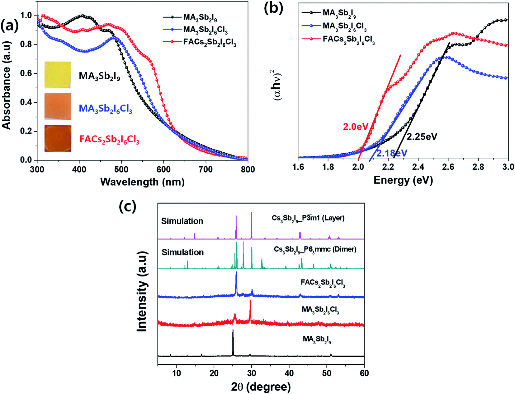 | ||
| Fig. 1 (a) UV-visible absorption spectra: inset = photographs of the MHP films, (b) Tauc plots, and (c) XRD patterns of MA3Sb2I9, MA3Sb2I6Cl3, and FACs2Sb2I6Cl3 MHP films. | ||
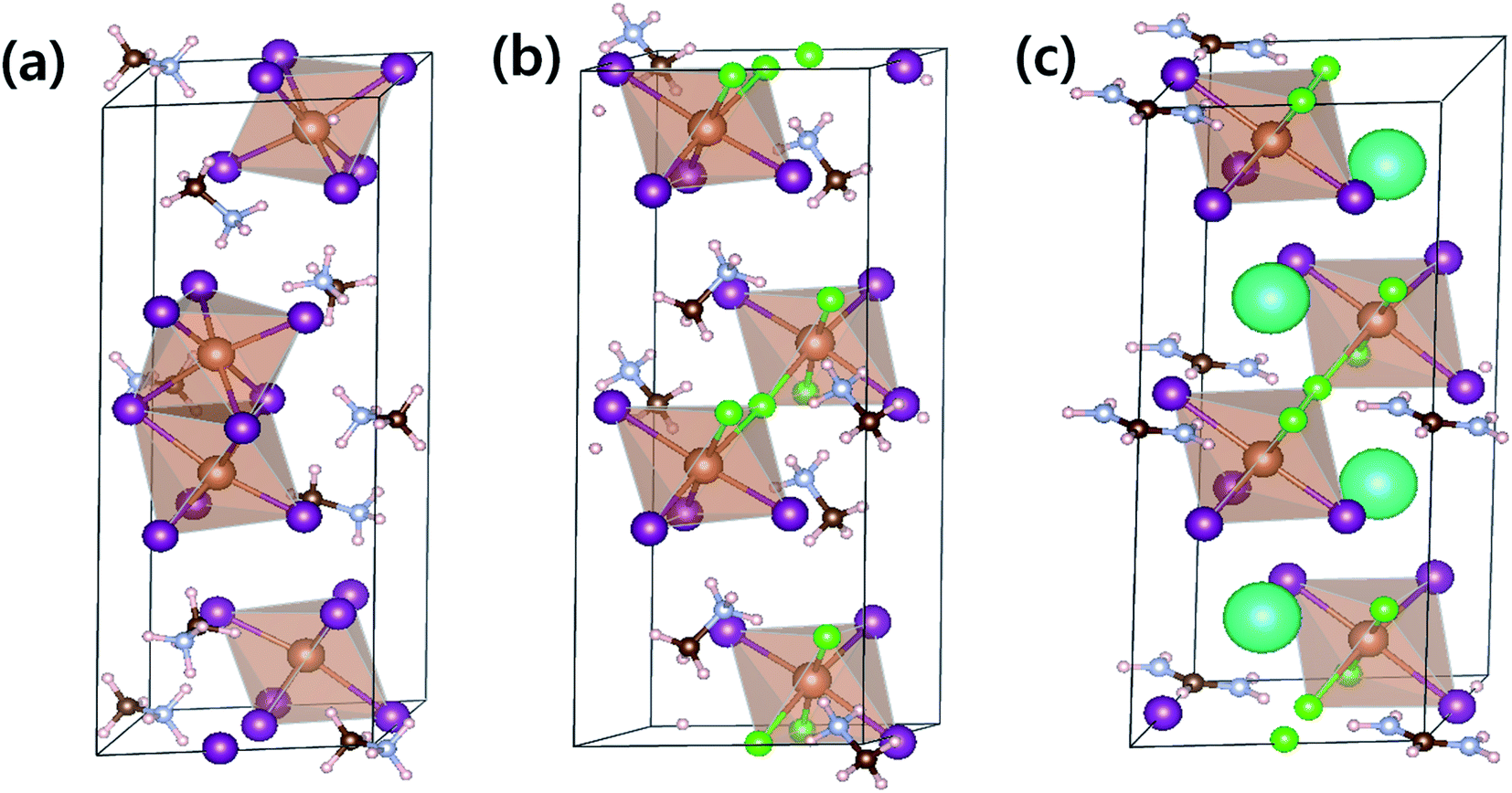 | ||
| Fig. 2 Lattice structures of (a) MA3Sb2I9 (P63/mmc), (b) MA3Sb2I6Cl3 (Pm1), and (c) FACs2Sb2I6Cl3 (Pm1). Pink/brown/light gray/mint/light brown/green/purple spheres represent H/C/N/Cs/Sb/Cl/I respectively. | ||
To understand the thermodynamic origins of dual-site mixing induced phase stabilization for the layered structures, we adopted density functional theory (DFT) using the Vienna ab initio simulation package (VASP).25,26 Details of DFT calculations are summarized in the ESI Section.† Optimized lattice structures for MA3Sb2I9 (P63/mmc), MA3Sb2I6Cl3 (Pm1), and FACs2Sb2I6Cl3 (Pm1) are expressed in Fig. 2 and Table 1.
| Calculated lattice structures | Calculated volume/FU Å3 | Calculated band gap (eV) | ||
|---|---|---|---|---|
| PBEsol | PBEsol + SOC | |||
| MA3Sb2I9 (P63/mmc) | a = 8.637 Å, b = 8.475 Å, c = 21.246 Å, α = 90.8°, β = 89.4° γ = 120.0° | 673.4 | 1.82 | 1.69 |
| MA3Sb2I6Cl3 (Pm1) |
a = 8.077 Å, b = 8.362 Å, c = 10.233 Å, α = 89.9°, β = 90.8° γ = 119.05° | 604.1 | 1.70 | 1.55 |
| FACs2Sb2I6Cl3 (Pm1) |
a = 8.145 Å, b = 8.403 Å, c = 9.888 Å, α = 91.1°, β = 91.1° γ = 118.7° | 593.4 | 1.67 | 1.52 |
Band structures and density of states (DOS) are represented in Fig. 3(a–c). The 2D layer structured perovskites (Pm1) exhibit a more direct band gap like feature comparing with the 0D dimer structured perovskites (P63/mmc). The calculated band gaps of the perovskites with and without spin orbital coupling (SOC) are summarized in Table 1. The FACs2Sb2I6Cl3 (Pm1) shows the smallest band gap regardless of SOC considering. The band gap narrowing by I–Cl mixed halide perovskites is attributed to the change of the lattice symmetry, i.e., the phase change from P63/mmc to Pm1.17,22,27 The reduced band gap for the FACs2Sb2I6Cl3 (Pm1) can be explained by its shorter bond length than the other perovskites. The volume per formula unit (FU) of FACs2Sb2I6Cl3 (Pm1) is the smallest even though their lateral dimension is slightly larger than MA3Sb2I6Cl3 (Pm1) as listed in Table 1. The ionic radius of Cs is the shortest among Cs, MA, and FA so that the volume of FACs2Sb2I6Cl3 can be the smallest. Accordingly, we can think that the FACs2Sb2I6Cl3 has the shortest bond length due to its smallest volume.
 | ||
| Fig. 3 Band structures (left panel) and projected density of states (PDOS) of (a) MA3Sb2I9 (P63/mmc), (b) MA3Sb2I6Cl3 (Pm1), and (c) FACs2Sb2I6Cl3 (Pm1). Valence band maximum energy is set to 0. Spin orbit coupling is included during the calculation. Calculated band gaps are underestimated than those of experimental values. (d) Solution energy changes by A-site mixing of FAxCs3−xSb2I6Cl3. The dotted lines are connecting the lowest energy states and dispersed symbols represent individual calculation result to obtain optimum lattice structures. | ||
The role of A-site binary mixing on the stabilization of 2D layered structure is investigated by calculating solution energies as shown in Fig. 3(d). The solution energies of layered structures are smaller than those of dimer structures. The FACs2Sb2I6Cl3 (Pm1) has only 28 meV FU−1 of solution energy, which can be spontaneous reactions considering the contribution of configurational entropy.28,29 The DFT calculations clearly show that the dual-site mixing on A and X in A3Sb2X9 perovskite can be an efficient way to improve the stability of 2D layer structure and band gap modulation.
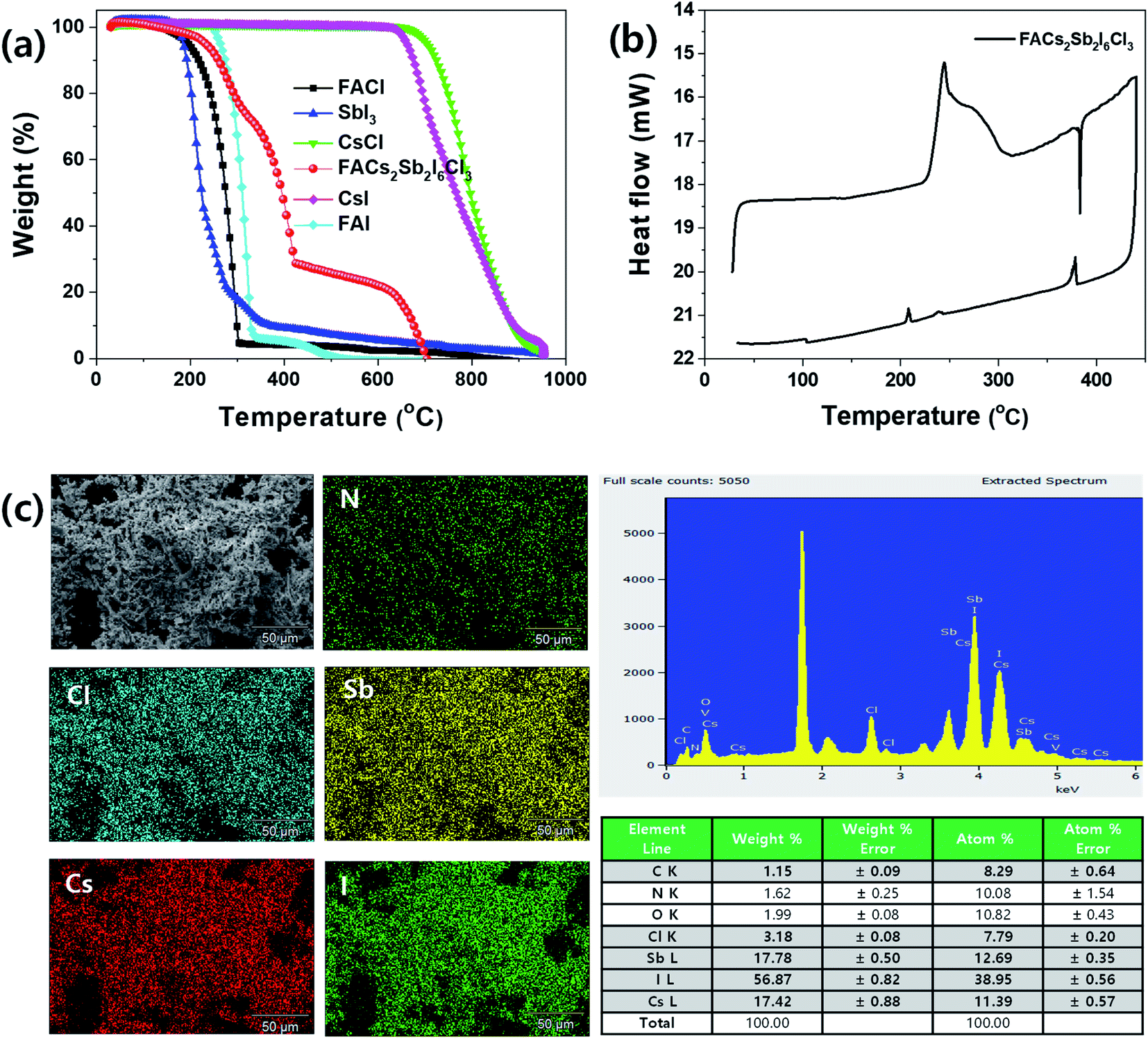
To check thermal properties of the dual-site mixed FACs2Sb2I6Cl3 MHP film, we checked thermal gravimetric analysis (TGA) thermogram and differential scanning calorimetry (DSC) as shown in Fig. 4(a) and (b). Here, we prepared the FACs2Sb2I6Cl3 MHP powder by mixing 1![[thin space (1/6-em)]](https://www.rsc.org/images/entities/char_2009.gif) :2:2 molar ratio of FACl:CsCl:SbI3 instead of mixing 1:2:1:1 molar ratio of FAI:CsI:SbI3:SbCl3 because the SbCl3 is more easily sublimed than the SbI3. The corresponding XRD patterns in Fig. S2† indicate that both samples have layered structures. The TGA and DTA (differential thermal analysis) spectra in Fig. 4(a) and S3† indicate that the FACl and SbI3 begins to be decomposed at ∼200 °C, whereas the CsCl starts to be decomposed at ∼700 °C. The prepared FACs2Sb2I6Cl3 MHP powder begins to be decomposed at ∼230 °C. This implies that the perovskite phase is formed by mixing of 1:2:2 molar ratio of FACl:CsCl:SbI3. The weight% of FACl:CsCl:SbI3 in FACs2Sb2I6Cl3 is 5.67:23.67:70.66 so the FACl and SbI3 are decomposed at 230–420 °C and the CsCl is decomposed over 420 °C. The higher decomposition temperature of prepared MHP powder at 150–300 °C than the pure FACl and the lower decomposition temperature of the powder at > 420 °C than the pure CsCl confirms that the new interaction bonding of FA–I and Cs–I is formed by formation of perovskite phase because their decomposition temperatures are FACl < FAI and CsI < CsCI in Fig. 4(a). Some I in the SbI3 might be replaced with Cl so its composition might be SbI3−xClx. Therefore, The FACs2Sb2I6Cl3 MHP powder might show an inflection point at ∼310 °C. The DSC spectrum in Fig. 4(b) shows that the synthesized FACs2Sb2I6Cl3 MHP powder begins to be decomposed at ∼230 °C, which is consistent with the TGA result.
:2:2 molar ratio of FACl:CsCl:SbI3 instead of mixing 1:2:1:1 molar ratio of FAI:CsI:SbI3:SbCl3 because the SbCl3 is more easily sublimed than the SbI3. The corresponding XRD patterns in Fig. S2† indicate that both samples have layered structures. The TGA and DTA (differential thermal analysis) spectra in Fig. 4(a) and S3† indicate that the FACl and SbI3 begins to be decomposed at ∼200 °C, whereas the CsCl starts to be decomposed at ∼700 °C. The prepared FACs2Sb2I6Cl3 MHP powder begins to be decomposed at ∼230 °C. This implies that the perovskite phase is formed by mixing of 1:2:2 molar ratio of FACl:CsCl:SbI3. The weight% of FACl:CsCl:SbI3 in FACs2Sb2I6Cl3 is 5.67:23.67:70.66 so the FACl and SbI3 are decomposed at 230–420 °C and the CsCl is decomposed over 420 °C. The higher decomposition temperature of prepared MHP powder at 150–300 °C than the pure FACl and the lower decomposition temperature of the powder at > 420 °C than the pure CsCl confirms that the new interaction bonding of FA–I and Cs–I is formed by formation of perovskite phase because their decomposition temperatures are FACl < FAI and CsI < CsCI in Fig. 4(a). Some I in the SbI3 might be replaced with Cl so its composition might be SbI3−xClx. Therefore, The FACs2Sb2I6Cl3 MHP powder might show an inflection point at ∼310 °C. The DSC spectrum in Fig. 4(b) shows that the synthesized FACs2Sb2I6Cl3 MHP powder begins to be decomposed at ∼230 °C, which is consistent with the TGA result.
 | ||
| Fig. 4 (a) Thermogravimetric analysis (TGA) spectra of FACl, SbI3, CsCl, CsI, FAI and FACs2Sb2I6Cl3 MHP powder, (b) differential scanning calorimeter (DSC) spectra of FACs2Sb2I6Cl3 MHP powder, and (c) energy disperse X-ray spectroscopy (EDS) elemental mapping and spectra of FACs2Sb2I6Cl3 MHP film. | ||
Fig. 4(c) is energy dispersive X-ray spectroscopy (EDS) elemental mapping and spectrum of the synthesized FACs2Sb2I6Cl3 MHP powder. The Cl, Sb, Cs, and I elements were well dispersed in the EDS elemental mapping image so we can think that the perovskite phase is created. However, the EDS spectrum indicates that the formed FACs2Sb2I6Cl3 MHP powder is halide deficient because the molar ratio of Cs:Sb:I:Cl was 1.80:2.00:6.14:1.23. This might be attributed to the heat-treatment of the FACs2Sb2I6Cl3 MHP powder at 200 °C for 5 min under nitrogen atmosphere or the oxidation of SbI3. The UV-visible absorption spectra of the heat treated FACs2Sb2I6Cl3 MHP films at 110 °C, 150 °C, and 200 °C for 5 min under N2 atmosphere and photographs of corresponding films were shown in Fig. S4(a).† This clearly shows that the film is slightly darken by heat-treatment at 200 °C and its on-set absorption band edge is also slightly red-shifted. Their corresponding XRD patterns in Fig. S4(b)† indicate that their crystalline structures are maintained to 2D layer structure irrespective of heat-treatment temperature. The slightly narrowed XRD peaks by heat-treatment indicate that their crystallinities are slightly improved.
The electronic structure of synthesized FACs2Sb2I6Cl3 MHP film was analyzed by ultraviolet photoelectron spectroscopy (UPS) spectrum as shown in Fig. 5(a). The zoom-up UPS spectra confirm that the onset photoemission and valence band edge is 16.25 eV and 1.50 eV, respectively. Therefore, a calculated valence band maximum (VBM) energy (EVBM = hν − Ecut-off + ΔEVB, where hν = 21.22 eV for He I, Ecut-off = 16.25 eV, and ΔEVB = 1.50 eV) of the FACs2Sb2I6Cl3 MHP film is −6.47 eV. The calculated conduction band minimum (CBM) energy is −4.47 eV because its bandgap is 2.0 eV in Tauc plot. The band energy diagram of the TiO2 electrode based FACs2Sb2I6Cl3 MHP SC was shown in Fig. 5(b). The mesoscopic TiO2 based MHP SC was composed of FTO/bl-TiO2/m-TiO2/MHP/PTAA/Au. A representative SEM cross-sectional image of mesoscopic TiO2 based MHP SC was shown in Fig. 5(c). The SEM surface of MA3Sb2I9, MA3Sb2I6Cl3, and FACs2Sb2I6Cl3 film on m-TiO2/bl-TiO2/FTO substrate were shown in Fig. 5(d–f), respectively. The current density–voltage (J–V) curves of mesoscopic MA3Sb2I9, MA3Sb2I6Cl3, and FACs2Sb2I6Cl3 MHP SCs in Fig. 5(g) indicate that the dual-site mixed FACs2Sb2I6Cl3 MHP SC have the highest PCE than the other MHP SCs. A short-circuit current density (Jsc), open-circuit voltage (Voc), fill factor (FF), and PCE of FACs2Sb2I6Cl3 MHP SC was 2.88 mA cm−2, 0.59 V, 61.6%, and 1.05% at 1 sun condition. Their photovoltaic parameters were summarized in Table 2. Average photovoltaic properties of 16 samples for each device were shown in Fig. S5.† The FACs2Sb2I6Cl3 MHP SC did not show significant J-V hysteresis with respect to the scan direction as shown in Fig. S6.† Their external quantum efficiency (EQE) spectra were shown in Fig. 5(h). Although their PCEs are still very poor, it is clear that the dual site-mixed A3Sb2X9 MHP SCs have 2D layer structure and narrower bandgap. To check the stabilities of MA3Sb2I9, MA3Sb2I6Cl3, and FACs2Sb2I6Cl3 MHP SCs, we tracked the maximum power points (MPPs) of un-encapsulated devices for 60 min under continuous light soaking at 1 sun as shown in Fig. 5(i). This clearly shows that the FACs2Sb2I6Cl3 MHP SC has good stability.
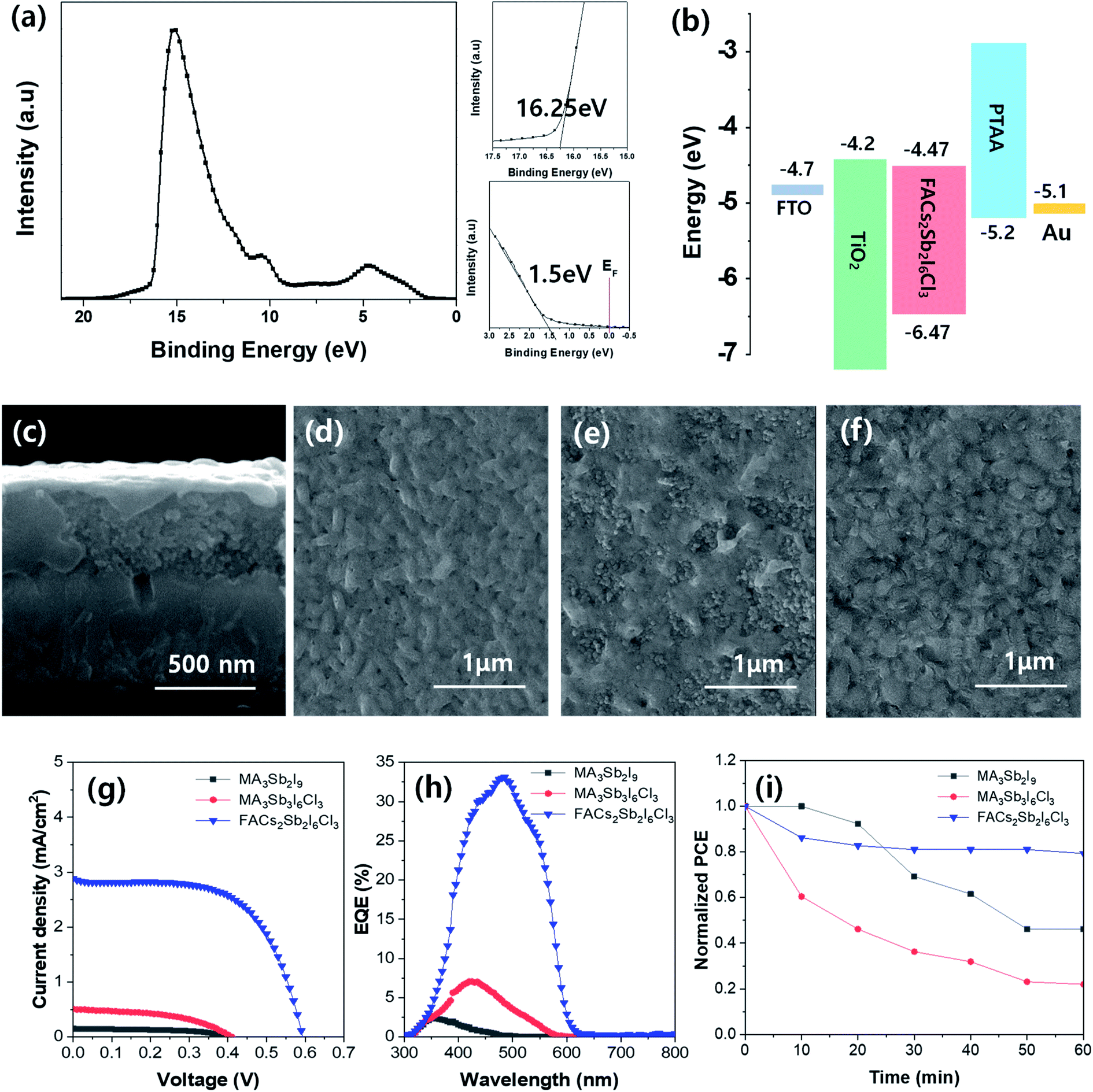 | ||
| Fig. 5 (a) Ultraviolet photoelectron spectroscopy (UPS) spectrum of FACs2Sb2I6Cl3 MHP film, (b) energy band diagram of MHP SC, (c–f) representative SEM cross-sectional image of MHP SC (c) and SEM surface images (d–f) of FTO/bl-TiO2/m-TiO2/MHP ((d) MA3Sb2I9, (e) MA3Sb2I6Cl3, and (f) FACs2Sb2I6Cl3), and (g–i) photovoltaic properties of MHP SCs: (g) current density–voltage curves, (h) EQE spectra, and (i) stabilities of mesoscopic MA3Sb2I9, MA3Sb2I6Cl3, and FACs2Sb2I6Cl3 MHP SCs and planar FACs2Sb2I6Cl3 MHP SC. | ||
| Device | Jsc (mA cm−2) | Voc (V) | FF (%) | PCE (%) |
|---|---|---|---|---|
| MA3Sb2I9 | 0.162 | 0.40 | 55.0 | 0.03 |
| MA3Sb2I6Cl3 | 0.51 | 0.42 | 47.9 | 0.10 |
| FACs2Sb2I6Cl3 | 2.88 | 0.59 | 61.6 | 1.05 |
Conclusions
In summary, we could synthesize 2D layer structured FACs2Sb2I6Cl3 perovskite with narrower energy bandgap by dual-site mixing. The narrower bandgap of FACs2Sb2I6Cl3 perovskite than the 0D dimer structured MA3Sb2I9 and the 2D layer structured MA3Sb2I6Cl3 is attributed to the phase change from P63/mmc dimer structure to Pm1 layer structure due to the change of lattice symmetry by I–Cl mixed halide and the shorter bond length than the others due to the shortest ionic radius of Cs among Cs, MA, and FA. Consequently, the dual-site mixed FACs2Sb2I6Cl3 MHP SCs exhibited higher PCE of 1.05% at 1 sun conditions than the dimer structured MA3Sb2I9 MHP SCs and the layer structured MA3Sb2I6Cl3 MHP SCs.
Conflicts of interest
There are no conflicts to declare.Acknowledgements
This study was supported by the National Research Foundation of Korea (NRF) under the Ministry of Science, ICT & Future Planning (Basic Science Research Program (No. 2014R1A5A1009799), Nano-Material Technology Development Program (No. 2017M3A7B4041696) and the Technology Development Program to Solve Climate Change (No. 2015M1A2A2055631)) and the Ministry of Trade, Industry & Energy, Republic of Korea New & Renewable Energy Core Technology Program of the Korea Institute of Energy Technology Evaluation and Planning (KETEP) (No. 20183010013820).Notes and references
- A. Kojima, K. Teshima, Y. Shirai and T. Miyasaka, J. Am. Chem. Soc., 2009, 131, 6050 CrossRef CAS PubMed.
- M. M. Lee, J. Teuscher, T. Miyasaka, T. N. Murakami and H. J. Snaith, Science, 2012, 338, 643 CrossRef CAS PubMed.
- J. H. Noh, S. H. Im, J. H. Heo, T. N. Mandal and S. I. Seok, Nano Lett., 2013, 13, 1764 CrossRef CAS PubMed.
- J. H. Heo, S. H. Im, J. H. Noh, T. N. Mandal, C. S. Lim, J. A. Chang, Y. H. Lee, H. J. Kim, A. Sarkar, M. K. Nazeeruddin, M. Grätzel and S. I. Seok, Nat. Photonics, 2013, 7, 486 CrossRef CAS.
- N. J. Jeon, J. H. Noh, Y. C. Kim, W. S. Yang, S. Ryu and S. I. Seok, Nat. Mater., 2014, 13, 897 CrossRef CAS PubMed.
- W. S. Yang, J. H. Noh, N. J. Jeon, Y. C. Kim, S. Ryu, J. Seo and S. I. Seok, Science, 2015, 348, 1234 CrossRef CAS PubMed.
- J. H. Heo and S. H. Im, Nanoscale, 2016, 8, 2554 RSC.
- N. J. Jeon, H. Na, E. H. Jung, T. Y. Yang, Y. G. Lee, G. Kim, H. W. Shin, S. I. Seok, J. Lee and J. Seo, Nat. Energy, 2018, 3, 682 CrossRef CAS.
- NREL, https://www.nrel.gov/pv/assets/pdfs/best-research-cell-efficiencies.20191106.pdf, rev. 11.06.2019.
- A. Babayigit, A. Ethirajan, M. Muller and B. Conings, Nat. Mater., 2016, 15, 247 CrossRef CAS PubMed.
- Z. Shi, J. Guo, Y. Chen, Q. Li, Y. Pan, H. Zhang, Y. Xia and W. Hunag, Adv. Mater., 2017, 29, 1605005 CrossRef PubMed.
- F. Hao, C. C. Stoumpos, D. H. Cao, R. H. Chang and M. G. Kanatzidis, Nat. Photonics, 2014, 8, 489 CrossRef CAS.
- E. Jokar, C.-H. Chien, C.-M. Tsai, A. Fathi and E. W.-G. Diau, Adv. Mater., 2019, 31, 1804835 CrossRef PubMed.
- J. H. Heo, J. Kim, H. Kim, S. H. Moon, S. H. Im and K.-H. Hong, J. Phys. Chem. Lett., 2018, 9, 6024 CrossRef CAS PubMed.
- T. Krishnamoorthy, H. Ding, C. Yan, W. L. Leong, T. Baikie, Z. Zhang, M. Sherburne, S. Li, M. Asta, N. Mathews and S. G. Mhaisalkar, J. Mater. Chem. A, 2015, 3, 23829 RSC.
- W. Liao, D. Zhao, Y. Yu, C. R. Grice, C. Wang, A. J. Cimaroli, P. Schulz, W. Meng, K. Zhu, R.-G. Xiong and Y. Tan, Adv. Mater., 2016, 28, 9333 CrossRef CAS PubMed.
- B. Saparov, F. Hong, J.-P. Sun, H.-S. Duan, W. Meng, S. Cameron, I. G. Hill, Y. Yan and D. B. Mitzi, Chem. Mater., 2015, 27, 5622 CrossRef CAS.
- B.-W. Park, B. Philippe, X. Zhang, H. Rensmo, G. Boschloo and E. M. J. Johansson, Adv. Mater., 2015, 27, 6806 CrossRef CAS PubMed.
- J. H. Heo, M. H. Lee, D. H. Song, C. E. Song, J.-J. Lee, K.-H. Hong and S. H. Im, Nanosci. Nanotechnol. Lett., 2018, 10, 591 CrossRef.
- P. C. Harikesh, H. K. Mulmudi, B. Ghosh, T. W. Goh, Y. T. Teng, K. Thurumal, M. Lockrey, K. Weber, T. M. Koh, S. Li, S. Mhaisalkar and N. Mathews, Chem. Mater., 2016, 28, 7496 CrossRef CAS.
- J.-P. Correa-Baena, L. Nienhaus, R. C. Kurchin, S. S. Shin, S. Wieghold, N. T. P. Hartono, M. Layurova, N. D. Klein, J. R. Poindexter, A. Polizzotti, S. Sun, M. G. Bawendi and T. Buonassisi, Chem. Mater., 2018, 30, 3734 CrossRef CAS.
- F. Jiang, D. Yang, Y. Jiang, T. Liu, X. Zhao, Y. Ming, B. Luo, F. Qin, J. Fan, H. Han, L. Zhang and Y. Zhou, J. Am. Chem. Soc., 2018, 140, 1019 CrossRef CAS PubMed.
- F. Umar, J. Zhang, Z. Zin, I. Muhammad, X. Yang, H. Deng, K. Jahangeer, Q. Hu, H. Song, H. Song and J. Tang, Adv. Opt. Mater., 2018, 7, 1801368 CrossRef.
- X.-G. Zhao, J.-H. Yang, Y. Fu, D. Yang, Q. Xu, L. Yu, S.-H. Wei and L. Zhang, J. Am. Chem. Soc., 2017, 139, 2630 CrossRef CAS PubMed.
- G. Kresse and J. Hafner, Phys. Rev. B: Condens. Matter Mater. Phys., 1993, 47, 558 CrossRef CAS PubMed.
- G. Kresse and J. Furthmüller, Comput. Mater. Sci., 1996, 6, 15 CrossRef CAS.
- K.-H. Hong, J. Kim, L. Debbichi, H. Kim and S. H. Im, J. Phys. Chem. C, 2017, 121, 969 CrossRef CAS.
- F. Brivio, C. Caetano and A. Walsh, J. Phys. Chem. Lett., 2016, 7, 1083 CrossRef CAS PubMed.
- J. Jeon, T. Eom, E. Lee, S. Kim, S. Kim, K.-H. Hong and H. Kim, J. Phys. Chem. C, 2017, 121, 9508 CrossRef CAS.
Footnote |
| † Electronic supplementary information (ESI) available. See DOI: 10.1039/d0ra00787k |
| This journal is © The Royal Society of Chemistry 2020 |