
 Open Access Article
 This Open Access Article is licensed under a Creative Commons Attribution-Non Commercial 3.0 Unported Licence
Bistable non-volatile resistive memory devices based on ZnO nanoparticles embedded in polyvinylpyrrolidone
Hongyan Zhanga,
Xiaofeng Zhaob,
Jiahe Huanga,
Ju Baia,
Yanjun Houa,
Cheng Wang *ac,
Shuhong Wang*a and
Xuduo Baia
*ac,
Shuhong Wang*a and
Xuduo Baia
aSchool of Chemical Engineering and Materials, Heilongjiang University, Harbin 150080, P. R. China. E-mail: openair@163.com; wangc_93@163.com
bSchool of Electronic Engineering, Heilongjiang University, Harbin 150080, P. R. China
cSouth China Advanced Institute for Soft Matter Science and Technology, South China University of Technology, Guangzhou 510640, P. R. China
First published on 13th April 2020
Abstract
The resistive random access memory (RRAM) devices based on polyvinylpyrrolidone (PVP) and PVP:PVP:zinc oxide nanoparticle (ZnO NP) active layers have bistable electrical switching behavior. Herein, via a series of storage performance tests, it was proved that the ITO/PVP:ZnO/Al device has a higher ON/OFF current ratio and better memory performance than the ITO/PVP/Al device. Moreover, at 13 wt% concentration of ZnO NPs, optimal storage performance was obtained, the switch state current ratio significantly increased, and the threshold voltage obviously decreased. The conduction mechanism of the devices was further discussed. The device having inorganic nanoparticles embedded in the polymer has excellent storage performance, which has potential application value in data storage.
Introduction
With the development of the information storage industry, the resistive electrode/active layer/electrode capacitor configuration of resistive random access memory (RRAM) devices has attracted significant attention due to its facile manufacturing process, low manufacturing cost, high performance, low power consumption, fast switching speed, and strong nonvolatility.1,2 Research has shown that inorganic materials, small organic molecules, and conjugated polymers exhibit a resistive switching behavior. However, due to the relatively high sensitivity of inorganic materials and oligomer molecules to water and oxygen, the melting point of these materials is low and thus, these materials should be encapsulated to prevent damage from the environment.3,4 In addition, memory devices are vulnerable to damage during the manufacturing process. On the other hand, organic and polymer materials possess excellent properties such as electronic properties that can be adjusted by changing the molecular structure, easy processing, good scalability, high mechanical flexibility, and low manufacturing costs, which facilitate their application in non-volatile memory devices. Organic and polymer materials are commonly referred to as organic electrical bistable materials. Under an external electric field, these devices can switch between two different conductive states, a high resistance state and a low resistance state, which are equivalent to “0” and “1”, respectively, in binary systems.5,6 As a result, polymer-based memory devices have received extensive attention.In recent years, the main research direction of resistive switch memory is towards the fabrication of devices using organic/inorganic nanocomposites as an active layer. For instance, Gu et al.7 have reported the fabrication of a memory device with the reduced graphene oxide (rGO)/Ti3C2Tx-PVP/Au structure, which is a non-volatile rewritable device with excellent performance. Kim et al.8 have prepared a bipolar resistance switching device with ferroelectric (FE) P(VDF-TrFE) and a ZnO nanoparticle (NP) composite material as the active layer. In the nanocomposites composed of polymer/inorganic hybrid nanomaterials, the polymer works as an electro functional host or a supporting matrix.9 The nanocomposites reported in recent years mainly include poly(ethylene oxide),10 poly(N-vinylcarbazole) (PVK),11 polystyrene (PS),12 and polyfluorene (PFO).13 Compared with these polymers, polyvinylpyrrolidone (PVP) has the advantages of good electrical properties, moderate conductivity and charge transfer mechanism, non-toxicity, safety, high solubility in most aqueous solvents, good adhesion, and film formation; therefore, it has attracted special attention from researchers.14,15 Inorganic nanoparticles (NPs) interact with polymers as guest additives under an applied voltage. The distribution and concentration of additives in the blend memory material has a significant influence on the reversibility or volatility of the film resistor.16 To date, inorganic nanomaterials, including metal NPs,17,18 metal oxide NPs,19,20 sulfides,21,22 and carbon materials,23–25 have been widely investigated as a active layers of RRAM. Among these inorganic nanoparticles, n-type semiconductor ZnO NPs have attracted extensive attention due to their wide band gap (3.37 eV), strong electron mobility (∼120 cm2 V s−1), high excitation binding energy (60 meV), high melting point, excellent chemical stability, and good charge carrier transport performance. ZnO NPs have a natural band gap, in which a large number of vacancy point defects may also provide a possible way for charge capture. Due to their excellent properties and tendency to be doped with defects and impurities, wideband gap metal oxides can be used in memory devices. When ZnO NPs are embedded into a polymer as an active layer of a bistable memory device, they can work as a carrier trap.26–29
In this study, the effect of the concentration of ZnO NPs embedded in PVP on the device performance was investigated. A mixture of ZnO NPs and the PVP composite at different concentrations was prepared and equipped into a series of electrical storage devices; the as-fabricated devices were then compared with the indium tin oxide (ITO)/PVP/Al device. The results of all performance tests showed that the storage performance of the devices with embedded ZnO NPs was significantly improved, and the electric bistable switching behavior of the PVP:ZnO films could be adjusted by changing the content of ZnO NPs.
Experimental
Materials
ZnO NPs with a particle size of 10–30 nm and specific surface area of equal to or larger than 110 m2 g−1 were purchased from J&K and stored in a dry nitrogen environment. Other reagents were purchased from Sinopharm Co. Ltd.Fabrication of a sandwich-type memory device
At first, a 2 cm × 1 cm indium tin oxide (ITO) conductive glass substrate was preprocessed by ultrasonication with deionized water, detergent, acetone, and ethanol for 30 min each and then stored in a vacuum drying oven for 12 h at 60 °C. ZnO NPs at different concentrations were embedded in PVP, and the ZnO NP-embedded PVP samples were used as the active layer of devices. PVP was dissolved in ethanol under stirring to prepare a solution with a concentration of 3 mg mL−1, which was filtered through a syringe filter (polytetrafluoroethylene, 0.22 μm) to prepare a homogeneous solution. To manufacture the blended composites, ZnO NPs were dispersed in ethanol and subjected to ultrasonication for 1 hour to prepare ZnO ethanol dispersions with different concentrations. Then, the ZnO dispersion and the pre-treated PVP solution were mixed at equal volumes, and the mixture was stirred for 2 hours. The ZnO NPs were randomly distributed throughout the entire host polymer PVP. Table 1 shows the different dosages of various components in the composite film samples. The mixed solutions were spin-coated on the ITO substrate at 900 rpm for 15 s and then at 3000 rpm for 45 s. After this, the semi-finished product was dried in a vacuum oven at 60 °C for 2 hours to remove the residual solvent. Before vacuum aluminizing, the thicknesses of the PVP and PVP:ZnO films were measured by a scanning electron microscope (SEM, Hitachi S3400). An Al electrode with a diameter of about 200 μm was coated onto the active layer by vacuum thermal evaporation at 7.5 × 10⁻⁷ torr. The schematic of the device with a sandwich structure is shown in Fig. 1.| Sample | ZnO content in the ethanol solution (mg mL−1) | Volume of the ZnO solution (mL) | Volume of the PVP ethanol solution (3 mg mL−1) | ZnO content in the composite film (wt%) |
|---|---|---|---|---|
| A | 0.00 | 0 | 1 | 0 |
| B | 0.13 | 1 | 1 | 4 |
| C | 0.26 | 1 | 1 | 8 |
| D | 0.40 | 1 | 1 | 12 |
| E | 0.44 | 1 | 1 | 13 |
| F | 0.48 | 1 | 1 | 14 |
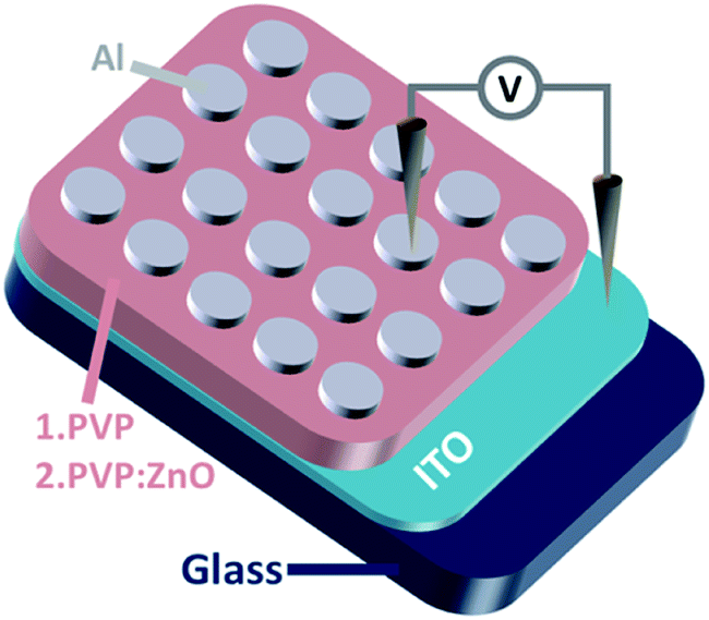 | ||
| Fig. 1 Schematic structure of the memory device. | ||
Results and discussion
Microscopy characterization of devices
Scanning electron microscopy (SEM) was performed on the cross-section of the device structure and the film thicknesses of the two active layers. According to Fig. 2(a) and (b), the device structure is glass, ITO, and active layer, which are clearly visible from bottom to top. Uniform thicknesses of the active layers of PVP and PVP:ZnO were observed, which were 104.8 nm and 96.8 nm, respectively. The dispersion of ZnO NPs was observed by transmission electron microscopy (TEM) (Fig. 2(c)). The TEM image shows that the ZnO NPs are uniformly and randomly distributed in the active layer. The results show that the two materials are homogeneously mixed. Fig. 2(d) displays the X-ray diffraction (XRD) patterns of the ZnO NPs. The peaks in the figure correspond to the (100), (002), (101), (102), (110), (103), (200), (112), (201), and (202) crystal planes of ZnO NPs. All these peaks can be indexed to hexagonal ZnO (JCPDS 36-1451). | ||
| Fig. 2 Cross-section SEM images of the devices based on the (a) PVP and (b) PVP:ZnO (13 wt%) composite films. (c) TEM image of PVP:ZnO; and (d) XRD pattern of ZnO NPs. | ||
Performances of the ITO/PVP/Al memory device
The current–voltage characteristic curves can reveal the storage characteristics of these devices. In order to investigate how the doping level affects the device performance, the performance of the device without doping (the ITO/PVP/Al device, sample A) was separately measured. As shown in Fig. 3(a), the four scanning steps constitute a classic I–V characteristic curve in various voltage ranges: from 0 V to −6 V, from −6 V to 0 V, from 0 V to 6 V, and from 6 V to 0 V. During the first scan, initially, the current slowly increased with an increase in the applied voltage. When the applied voltage reached −2.35 V, the current abruptly increased; that is, the device switched between the high resistance state (HRS) and the low resistance state (LRS). The conduction process represents the “writing” process in digital memory. The ON/OFF current ratio of the device was up to 2.4 × 10². The LRS was still observed in the second scan (sweep 2), i.e. the “reading” process. Then, in the 3rd sweep, when the applied positive bias voltage reached a certain value, the current suddenly decreased from the high conductive state (ON state) to the original low conductive state (OFF state), and the corresponding process is called “erasing”. In the last sweep, the curve shows a “rereading” process with a consistent trend of the OFF state and an outward extension. As abovementioned, the two-stage process of a sharp increase and then decrease in current is also referred to as “set” and “reset”, respectively. In addition, the rewritable electrical characteristics exhibited during the four-step scan depict the entire “write–read–erase–reread” (WRER) cycle, indicating a non-volatile characteristic and a flash-type memory behaviour of the device.30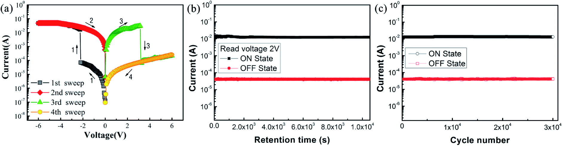 | ||
| Fig. 3 (a) I–V curves, (b) retention performance, and (c) endurance performance of the ITO/PVP/Al device. | ||
The endurance and retention performances of the device were also examined, as shown in Fig. 3(b) and (c). It can be observed from the figure that the current retains the initial value at a constant voltage of 2 V. No significant attenuation was observed for both the HRS and the LRS within 3 h, during which the ON/OFF current ratio was approximately 2.4 × 10². In addition, the device performance was maintained even after 3 × 10⁴ cycles of operation at the read pulse of 2 V. These results indicate the good stability and reliability of these devices.
Characterization of the ITO/PVP:ZnO/Al memory devices
Based on the measurement results of the abovementioned pure polymer material as the active layer, to investigate how the ZnO NP concentration affect the memory performance of the device, PVP:ZnO mixtures with various concentrations were prepared. Fig. 4(a) displays the I–V characteristic curves of all ZnO NP-doped ITO/PVP:ZnO/Al devices. Similar to the case of the ITO/PVP/Al device, in the voltage sweep range from 0 V to −6 V, the current suddenly increased from the OFF state to the ON state, and the opposite trend was observed during the scan from 0 V to 6 V. The abrupt changes in current throughout the cycle allowed the device to switch between the LRS and the HRS, and the electrical memory characteristic curve reveals a homogeneous flash phenomenon. The threshold voltages of the samples B, C, D, E, and F are −2.20 V, −1.60 V, −1.35 V, −0.60 V, and −0.85 V and the ON/OFF current ratios are 3.3 × 10², 1.3 × 10³, 4.5 × 10³, 3.9 × 10⁴, and 4.6 × 10³, respectively. The sample E has the highest switching current ratio and the lowest threshold voltage.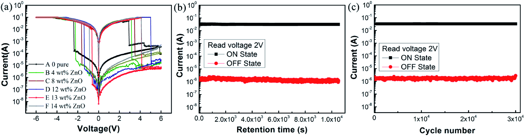 | ||
| Fig. 4 (a) I–V curves of ITO/PVP:ZnO/Al with different doping levels of ZnO NPs and (b) the retention performance and (c) endurance performance of the sample E-based device. | ||
The stability of the sample E-based device was tested, and the results are shown in Fig. 4(b). Under an atmosphere with the initial voltage of 2 V and the ON/OFF current ratio of 3.8 × 10⁴, the two state currents could remain unchanged within 3 h, indicating the excellent stability of this device. In addition, Fig. 4(c) shows that the cycle period at a 2 V pulse reached 3 × 10⁴, indicating that the read cycle had no effect on the HRS and LRS. The stability performance of the ITO/PVP:ZnO/Al storage device is not inferior to that of the pure polymer storage device. Overall, compared with the ITO/PVP/Al memory device, the devices doped with ZnO NPs performed better: the threshold voltage had a downtrend in the range from −2.2 V to −0.6 V and the ON/OFF current ratio increased by two orders of magnitude.
In addition to the abovementioned comparative experiments, the effects of the ZnO NP doping concentration on the threshold voltage and switching ratio were investigated by a double Y curve. Fig. 5(a) shows that the devices doped with ZnO NPs at different concentrations exhibited varying degrees of memory performance in terms of the threshold voltage and ON/OFF current ratio. Therefore, the doping concentration of ZnO NPs is a key factor in lowering the threshold voltage and increasing the ON/OFF current ratio. As the doping concentration increased, the ON/OFF current ratio first increased and then decreased after reaching a maximum value. This phenomenon can be explained by the good electrical conductivity of ZnO NPs, which are dispersed on the surface of the film to form an electron transport path. The effective distance of the ZnO NPs decreased with an increase in the doping concentration. When the effective distance was smaller than the diameter of a single ZnO NP, the uniform two-phase interface would help to form more electron transport paths. When the threshold voltage was reached, a large number of electrons passed through the ZnO NPs, causing an increase in the switching current ratio.31
 | ||
| Fig. 5 (a) The ON/OFF current ratio as well as threshold voltage of the ZnO NP-doped ITO/PVP:ZnO/Al devices. (b) The ON/OFF current ratio of the ITO/PVP:ZnO/Al and ITO/PVP/Al devices. | ||
Table 2 summarizes the memory characteristics of the ITO/composite/Al sandwich structures based on different ZnO composites, which have been reported to exhibit best performance in the literature. According to the summary results presented in Table 2, it is found that when compared with the device based on the polymer matrix materials PVK, PFO, and PEO, the device proposed in this study has a larger ON/OFF current ratio and lower threshold voltage and is expected to have high memory performance and low power consumption in practical applications; thus, this device is better than the devices based on other ZnO composites.
| Mixing material | ZnO content | Memory type | ON/OFF ratio | Threshold voltage | Reference |
|---|---|---|---|---|---|
| Polyvinylpyrrolidone | 13 wt% | Flash | 104 | −0.6 V | This paper |
| Poly(ethylene oxide) | 9 wt% | Flash | — | — | 10 |
| Poly(9,9-dioctylfluorene-2,7-diyl) | 6 wt% | Flash | 103 | −1.1 V | 13 |
| Poly(9-vinylcarbazole) | 6 wt% | Worm | 103 | +1.0 V | 11 |
| Poly(9-vinylcarbazole) | 2 wt% | Worm | 103 | −1.8 V | 31 |
However, excessive doping concentration led to a reduction in the effective distance between ZnO NPs; this affected the transport of charge carriers along the electron path, making it difficult for the charge carriers to pass through the ZnO NPs and resulting in a decrease in the current ratio. The threshold voltage decreased with an increase in the doping concentration until a minimum was reached at the same concentration because a smaller distance between ZnO NPs enabled effective carrier transport at lower activation energy. Fig. 5(b) shows a comparison between the memory windows of the device with an optimum doping concentration (sample E-based device) and the ITO/PVP/Al device.
It can be observed that the flash window of the device with a doping concentration of 13 wt% has significantly improved. By controlling the switching state during the storage procedure, the misreading rate can be reduced. It can be observed in the figure that the reset voltage of the devices based on PVP:ZnO is higher as compared to that of the pure PVP devices. This is because in the devices with embedded ZnO NPs, more conductive paths are formed during the setup process, due to which the device requires more energy to break the conductive path, and thus, the reset voltage increases.
To check the uniformity during the operation of the device, we statistically distributed the set voltage (Vset) and reset voltage (Vreset) of 35 working cells (Fig. 6(a)). The data show that when compared with the case of the ITO/PVP/Al devices, the dispersion of Vset and Vreset of the ITO/PVP:ZnO/Al device is narrow, the coefficient of variation is low, and the distribution is uniform. Moreover, statistical analysis was performed on the current values of the two devices in the high-resistance and low-resistance states (Fig. 6(b)). As abovementioned, the distribution of Vset and Vreset is still narrow for the ITO/PVP:ZnO/Al device, indicating that the device with embedded ZnO NPs has better operational uniformity.32,33
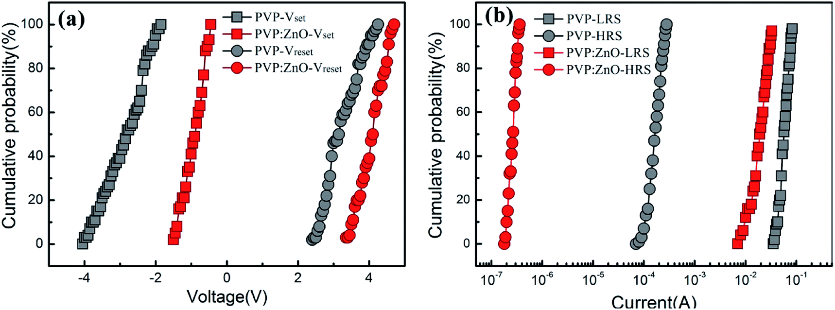 | ||
| Fig. 6 Statistical distribution of the switching parameters of devices: (a) set voltages (Vset) and reset voltages (Vreset) and (b) current values in the ON and OFF states. | ||
Mechanism of the ITO/PVP/Al and ITO/PVP:ZnO/Al memory devices
To further explore the conduction mechanism of devices, the I–V characteristic curve was obtained using the log–log plot. Fig. 7 shows the linearly fitted curve of the ITO/PVP:ZnO/Al device (sample E-based device) in the HRS and LRS. Meanwhile, a schematic corresponding to each stage is shown in Fig. 8 for explaining the conduction mechanism. Fig. 7 shows that the slope of the fitted curve for the ITO/PVP:ZnO/Al device in the OFF state at a low voltage is 0.99 (set). The ZnO NPs distributed in PVP worked as a capture center, indicating that the electrons were occupied by a defect level and impurity level capture trap (Fig. 8(a)). The small number of carriers generated by thermionic emission at this stage had a main effect on charge transport. As the voltage increased, the traps were filled due to the transfer of charges between PVP and ZnO NPs (Fig. 8(b)). Then, the traps were completely filled as the applied voltage increased (Fig. 8(c)). As a result, the electron concentration became higher in the active layer of the PVP:ZnO-based device. The slope of the fitted curve is 2.01, and the relationship between I and V follows a square law (I ∝ V2), indicating that the conduction behavior follows the Child's law. As a result, the switching memory behavior of the device was guided by the space-charge-limited current (SCLC). When the applied voltage exceeded the threshold voltage, due to the higher electron concentration, the number of carriers injected into the active layer exponentially increased; this formed a conductive path in the active layer that would cause an increase in the current (Fig. 8(d)). The device switched between the OFF state and the ON state (slope = 0.97), indicating that the device exhibited an ohmic behavior (I ∝ V) in the ON state. Moreover, the PVP dielectric material used as a substrate exhibited insulating property, and the charge trapped by the ZnO NPs after power-off was retained, thereby making the memory device highly conductive and non-volatile. After applying a reverse voltage, the trapped charge would be released. Subsequently, the trapped charge-induced internal electric field disappeared, and the device switched to the initial HRS.34–36 | ||
| Fig. 7 Linear fitting and corresponding slopes for the sample E-based ITO/PVP:ZnO/Al device: (a) set and (b) reset. | ||
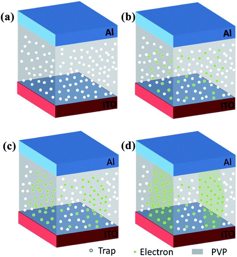 | ||
| Fig. 8 Schematic of the switching process for the ITO/PVP:ZnO/Al device. (a) Traps in the unoccupied state. (b) Injected carriers trapped by ZnO. (c) Gradually and completely filled traps. (d) The formation of the conductive path. | ||
Fig. 9 illustrates the migration process of the carriers based on the energy level diagrams of the two devices. When a negative voltage was applied to the Al/PVP/ITO device, the energy barrier between the ITO electrode and the HOMO level was lower when compared with that between the Al electrode and the LUMO level. Therefore, the hole injection process of the ITO electrode was more convenient when compared with the electron injection process of the Al electrode. With an increase in the voltage, holes were slowly injected into the HOMO from ITO and distributed along the polymer chain. The barrier between the LUMO and the Al electrode prevented electron migration, resulting in a slow increase in the current at a low voltage. When the voltage reached the threshold voltage, the electrons could obtain sufficient energy to overcome the energy barrier and were then injected into the active layer; that is, the electrons were excited from the HOMO to the LUMO orbital, causing an instantaneous increase in the current, and the state was switched to the LRS. The carriers were able to freely move between the two electrodes to form a conductive filament. After applying a reverse voltage and operating the device for a certain period of time, the injected charges would exceed and produce additional heat. Excessive current caused a repulsive coulomb interaction between the trapped charges in the organic active layer and interface to cut off the conductive path, after which the device returned to its original state. Furthermore, the molecular electrostatic potential (ESP) isosurface of PVP was simulated by DFT, as showed in Fig. 9(b). A continuous positive ESP (blue) is observed on the polymer backbone as an open channel for carrier transport. However, the negative ESP region (red) generated by the ketone group is regarded as a charge trap that impedes carrier transport. When the voltage is low, it is difficult for the carriers to obtain sufficient energy to overcome the potential barrier. Therefore, the memory device remains in the OFF state. When the voltage is increased, the carriers can acquire sufficient energy to fill the traps such that the device can be converted from the HRS to the LRS. The captured carrier can be stabilized by a charge transfer process, resulting in a charge separation state. However, there is only one negatively charged group in the main chain of PVP, and there is no twisted configuration in the main chain of this molecule. Therefore, the charge transfer process cannot maintain the charge separation state. Moreover, when a reverse voltage is applied, the captured carriers can be restored to the original state, and the device returns to the HRS, thereby exhibiting a flash-type switching behaviour.37,38
 | ||
| Fig. 9 (a) Energy level diagrams for the devices based on PVP. (b) The DFT-calculated molecular ESP. (c) The energy band diagrams of the ITO/PVP:ZnO/Al device. | ||
As the polymer exhibits a limited charge transport capability, ZnO was introduced for enhancing the charge injection capability and capture performance of the device. According to the previously reported studies, the band gap of ZnO NPs ∼ 3.3 eV.33,39 As the voltage increased, the carriers were injected into the device from the Al electrode via hole injection, followed by being trapped by ZnO for the formation of a space charge layer. When the voltage reached the threshold voltage, the carriers overcame the energy barrier and were injected into the polymer LUMO energy level along ZnO. As a result, the current sharply increased. The content of ZnO NPs in the device affected the effective distance of adjacent ZnO NPs, which in turn promoted the trapping behavior of charge carriers, leading to a difference in the conductive behavior of the device. Accordingly, extra heat generated by excess charge conduction during the reset process would cause the conductive path to rupture, and thereby, non-volatile bistable memory would be obtained.40,41
Conclusions
In this study, PVP:ZnO composite materials were used to fabricate electrical bistable resistive memory devices by the spin coating and evaporation coating technology. The influence of the concentration of ZnO NPs on the device was investigated, and different non-volatile electronic bistable resistance memory devices were obtained. As demonstrated by the experimental results, the ITO/PVP:ZnO/Al memory device displayed a classic conductance switching behavior, and the effects on the rewritable flash memory remained unchanged. On the basis of these memory cells, numerous resistance conversion characteristics were discovered. The device showed excellent electronic memory characteristics. Compared with the case of the ITO/PVP/Al device, for the ITO/PVP:ZnO/Al device, the switching ratio was improved by two orders of magnitude (from 2.4 × 10² to 3.9 × 10⁴) and a low threshold voltage was achieved (from −2.35 V to −0.60 V), which ensured a low misreading rate and rapid response. In addition, as demonstrated by the retention characteristics, the ITO/PVP:ZnO/Al device exhibited strong stability at a continuous voltage of 2 V for 3 h, and the continuous reading period at 2 V exceeded 3 × 10⁴ consecutive reading cycles without any decay. According to the abovementioned results, the proposed device has a low threshold voltage, high switching rate, and excellent stability; thus, the PVP:ZnO film has a promising and reliable role in the next-generation high storage density resistive random access memory.Conflicts of interest
The authors declare no conflict of interest.Acknowledgements
The authors are grateful to the National Natural Science Foundation of China (grant numbers 51527804 and 51973051), Heilongjiang University JMRH project (HDJMRH201913), and Natural Science Foundation of Heilongjiang Province of China (grant number: B2017010) for their support.Notes and references
- P. Zhang, B. Xu, C. Gao, G. Chen and M. Gao, ACS Appl. Mater. Interfaces, 2016, 8, 30336–30343 CrossRef CAS PubMed.
- B. Sun, X. Zhang, G. Zhou, T. Yu, S. Mao and S. Zhu, J. Colloid Interface Sci., 2018, 520, 19–24 CrossRef CAS PubMed.
- G. Chen, P. Zhang, L. Pan, L. Qi, F. Yu and C. Gao, J. Mater. Chem. C, 2017, 5, 9799–9805 RSC.
- B. Zhang, T. Cai, S. Li, X. Zhang, Y. Chen and K. G. Neoh, J. Mater. Chem. C, 2014, 2, 5189–5197 RSC.
- P. Y. Lai, Appl. Phys. Lett., 2008, 93, 274–276 Search PubMed.
- R. G. Hicks, Nat. Chem., 2011, 3, 189–191 CrossRef CAS PubMed.
- C. Gu and H. W. Mao, ACS Appl. Mater. Interfaces, 2019, 11, 38061–38067 CrossRef CAS PubMed.
- T. Y. Kim, Phys. Chem. Chem. Phys., 2018, 1–8 Search PubMed.
- J. Jung, et al., J. Ind. Eng. Chem., 2018, 64, 85–89 CrossRef CAS.
- J. P. Song and H. Z. Han, RSC Adv., 2017, 7, 54128–54135 RSC.
- K. Onlaor, T. Thiwawong and B. Tunhoo, J. Alloys Compd., 2018, 732, 880–886 CrossRef CAS.
- J. Ouyang, Org. Electron., 2014, 15, 1913–1922 CrossRef CAS.
- J. H. Huang, X. F. Zhao, H. Y. Zhang, J. Bai, S. H. Wang, C. Wang and D. G. Ma, RSC Adv., 2019, 9, 9392–9400 RSC.
- D. H. Kim, W. K. Kim and S. J. Woo, Org. Electron., 2017, 51, 156–161 CrossRef CAS.
- M. Ravi, Y. Pavani and K. Kumar, Mater. Chem. Phys., 2011, 130, 442–448 CrossRef CAS.
- Z. Zhou, H. W. Mao, X. J. Wang, T. Sun, Q. Chang, Y. Y. Chen, F. Xiu, Z. D. Liu and J. Q. Liu, Nanoscale, 2018, 10, 14824–14829 RSC.
- P. F. Lee and J. Y. Dai, Nanotechnology, 2010, 21, 295706 CrossRef CAS PubMed.
- K. Krishnan, T. Tsuruoka, C. Mannequin and M. Aono, Adv. Mater., 2016, 28, 640–648 CrossRef CAS PubMed.
- J. A. Ávila-Niño, M. Reyes-Reyes, O. Núñez-Olvera and R. López-Sandoval, Appl. Surf. Sci., 2018, 454, 256–261 CrossRef.
- T. Abhijith, T. V. Arun Kumar and V. S. Reddy, Nanotechnology, 2017, 28, 095203–095209 CrossRef CAS PubMed.
- L. Q. Wu, J. J. Guo, W. Zhong, W. J. Zhang, X. Kang, W. Chen and Y. W. Du, Appl. Surf. Sci., 2019, 463, 947–952 CrossRef CAS.
- F. Fan, B. Zhang, Y. Cao and Y. Chen, Nanoscale, 2017, 9, 2449–2456 RSC.
- Y. M. Sun, J. Lu and C. Ai, Phys. Chem. Chem. Phys., 2016, 18, 11341–11347 RSC.
- Y. N. Kim, D. Y. Yun, N. S. Arul and T. W. Kim, Org. Electron., 2015, 17, 270–274 CrossRef CAS.
- Q. Yang, X. K. Jiang, Y. Xin, X. F. Zhao, J. H. Huang, S. H. Wang, R. R. Zheng, D. G. Ma and C. Wang, RSC Adv., 2017, 7, 54431–54440 RSC.
- A. S. Zoolfakar, R. A. Kadir, S. Balendhran and X. J. Liu, Phys. Chem. Chem. Phys., 2013, 15, 10376–10384 RSC.
- B. Sun, X. Zhang, G. Zhou, T. Yu, S. Mao and S. Zhu, J. Colloid Interface Sci., 2018, 520, 19–24 CrossRef CAS PubMed.
- B. R. Lee, J. H. Park, T. H. Lee and T. G. Kim, ACS Appl. Mater. Interfaces, 2019, 11, 5215–5222 CrossRef CAS PubMed.
- T. Y. Kim, A. Gopinathan, Y. J. Son and S. H. Kim, Phys. Chem. Chem. Phys., 2018, 20, 16176–16183 RSC.
- J. Liu, Z. Zeng, X. Cao, G. Lu and L. H. Wang, Small, 2012, 22, 3517–3522 CrossRef PubMed.
- E. M. Zhao, D. U. Liu and B. Tunhoo, J. Mater. Sci.: Mater. Electron., 2017, 28, 11749–11886 CrossRef CAS.
- Y. T. Li and L. Yin, IEEE Electron Device Lett., 2019, 40, 1599–1601 CAS.
- D. I. Son, Nanotechnol, 2009, 20, 195203 CrossRef PubMed.
- J. C. Chen, C. L. Liu, Y. S. Sun and S. H. Tung, Soft Matter, 2012, 8, 526–535 RSC.
- K. Yan, B. Chen, H. Hu, S. Chen, B. Dong and X. Gao, Adv. Electron. Mater., 2016, 8, 1600160 CrossRef.
- H. Y. Zhang, X. F. Zhao, J. Bai, Y. J. Hou and S. H. Wang, Macromolecules, 2019, 52, 9364–9375 CrossRef CAS.
- Y. Xin, X. F. Zhao, H. Y. Zhang, S. H. Wang, C. Wang, D. G. Ma and P. F. Yan, Org. Electron., 2015, 16, 148–163 CrossRef.
- S. L. Lian, C. L. Liu and W. C. Chen, ACS Appl. Mater. Interfaces, 2011, 3, 4504–4511 CrossRef CAS PubMed.
- A. Kathalingam and J. K. Rhee, J. Electron. Mater., 2012, 41, 2162–2168 CrossRef CAS.
- A. Nakajima and D. Fujii, Appl. Phys. Lett., 2015, 106, 103302 CrossRef.
- Z. J. Liu, J. H. He, H. Zhuang, H. Li, N. J. Li and D. Y. Chen, J. Mater. Chem. C, 2015, 3, 9145–9153 RSC.
| This journal is © The Royal Society of Chemistry 2020 |