
 Open Access Article
 This Open Access Article is licensed under a Creative Commons Attribution-Non Commercial 3.0 Unported Licence
The improved performance and mechanism of solution-processed blue PhOLEDs based on double electron transport layers
Zijian Liu ab,
WeiYe Zhengab,
Peng Weiab,
Zheng Xuab,
Dandan Songab,
Bo Qiaoab and
Suling Zhao*ab
ab,
WeiYe Zhengab,
Peng Weiab,
Zheng Xuab,
Dandan Songab,
Bo Qiaoab and
Suling Zhao*ab
aKey Laboratory of Luminescence and Optical Information, Beijing Jiaotong University, Ministry of Education, Beijing 100044, China
bInstitute of Optoelectronics Technology, Beijing Jiaotong University, Beijing 100044, China
First published on 1st April 2020
Abstract
Performance improved solution-processed blue phosphorescent organic light emitting diodes (PhOLEDs) are demonstrated by adopting a double electron transport layer (ETL) strategy, which consists of TPBi and an additional Alq3 ETL. With the help of Alq3 ETL, the performance of the optimal device with a double ETL is significantly enhanced. The maximum luminance of OLEDs is improved from 6787 cd m−2 to 13![[thin space (1/6-em)]](https://www.rsc.org/images/entities/char_2009.gif) 054 cd m−2, and the maximum current efficiency is increased from 3.9 cd A−1 to 11.4 cd A−1. Furthermore, the difference of carrier injection in the two types of PhOLEDs is explored by using the transient electroluminescence measurement method. The results imply that double ETL can help to balance electron injection and carrier transport, reduce the interface charge accumulation, leading to a high efficiency. The PL decay of the emission layer with different ETL is detected to analyze the effect of the introduced second ETL layer and the interface on the exciton decay of the emission layer. The results show that the introduced interface in devices with a double ETL has an adverse effect on the exciton emission, which contributes to the serious efficiency roll-off of devices with a double ETL.
054 cd m−2, and the maximum current efficiency is increased from 3.9 cd A−1 to 11.4 cd A−1. Furthermore, the difference of carrier injection in the two types of PhOLEDs is explored by using the transient electroluminescence measurement method. The results imply that double ETL can help to balance electron injection and carrier transport, reduce the interface charge accumulation, leading to a high efficiency. The PL decay of the emission layer with different ETL is detected to analyze the effect of the introduced second ETL layer and the interface on the exciton decay of the emission layer. The results show that the introduced interface in devices with a double ETL has an adverse effect on the exciton emission, which contributes to the serious efficiency roll-off of devices with a double ETL.
1. Introduction
Organic light-emitting diodes (OLEDs) increasingly attract interest because of their great potential in the field of high-quality flat panel displays and solid-state lightning.1–4 For these applications, the luminance of OLEDs needs to reach 1000 cd m−2 (ref. 4–6) and even higher for the solid-state lighting devices.5,7 At present, the green OLEDs and the red OLEDs have achieved a high efficiency and long lifetime, which are enough for their applications. But how to improve the performance of the blue OLEDs is still a bottleneck, especially for solution-processed blue OLEDs.8–11In blue OLEDs, the electron transport layer (ETL) plays an important role in conducting electrons and blocking holes. Because most blue OLEDs are hole-dominant devices, the selection of appropriate ETL can optimize the electron injection and transportation then balance the carrier and reduce the leakage current to raise the brightness and efficiency of devices.12 But a poor ETL setting will make electrons difficult to inject, and lead to charge storage in the interface between the emitting layer (EML) and ETL, which may result in the exciton quenching.
Based on this problem, various methods have been investigated. Generally, double ETL has been widely used in various OLEDs to form a step barrier between the EML and cathode to enhance the electronic injection and improve the device efficiency, which not only avoids the device stability problem caused by mix host doping, but also saves the complex steps of cross-linking materials. In addition, it does not need to develop new host and guest materials, and avoids the defects of mixed evaporation.13 Yu Bai et al. inserted Gaq between Alq3 and TBADN to form a double ETL and fabricated blue OLED devices, which resulting in the increase of efficiency.14 Zhang et al. fabricated a blue OLED device using Bpy-OXD/Alq3 as a double ETL. The device showed much better chromaticity and less current-induced color shift as compared to the corresponding single ETL ones.15 Jang et al. used an double ETL of Bphen/Alq3 to realize a higher current density and luminance.16 Jia et al. demonstrated blue PhOLEDs containing a double ETL with the structure of Li(acac):PEI/ZnO:PI.17 This structure markedly improved the electron injection and transport and suppressed the triplet exciton quenching at the EML/ZnO interface, resulting in a lower driving voltage and doubled luminous efficiency compared with those of the control device. However, there is still a lack of an double ETL suitable for solution-processed 3,3′-bis(N-carbazolyl)biphenyl (mcp) system blue OLEDs.
In this paper, the double ETL structure of 1,3,5-tris(1-phenyl-1H-benzimidazol-2-yl)benzene (TPBi)/tris-(8-hydroxyquinoline)aluminum (Alq3) was introduced into the solution-processed blue PhOLEDs based on 3,3′-bis(N-carbazolyl)biphenyl:bis[(4,6-difluorophenyl)-pyridine-to-N,C2](picolinate) iridium(III) (mcp:Firpic) emitting layer (EML) in order to optimize the electron injection and expand the recombination region of excitons. Therefore, both the triplet–triplet annihilation (TTA) and triplet polaron quenching (TPQ) are expected to be restrained, which will improve the performance of the solution-processed blue PhOLED device.18–22 Therefore, to select two ETL materials for matching the energy barrier is a key issue to improve the electron injection and transport. The energy barrier between TPBi and cathode is 1.1 eV before introducing Alq3, and the electron injection barrier is reduced to 0.8 eV after the addition of Alq3,16,23–25 which can promote electron injection and balance charge carriers. The max luminance (Lmax) of 13054 cd m−2 and the max current efficiency (CEmax) of 11.4 cd A−1 are achieved in the optimal double ETL device, and at the luminance of 1000 cd m−2, the efficiency still maintain at 10.8 cd A−1. Compared with the single ETL device (Lmax is 6787 cd m−2, CEmax is 3.9 cd A−1), the double ETL system has done well in improving the performance of solution-processed blue OLED. Then the transient electroluminescence measurement was used to detect the carrier injection, capture and accumulation in the devices.
2. Experimental details
Materials
The hole-injection material of poly(3,4-ethylenedioxythiophene):poly (styrene sulfonate) (PEDOT:PSS), the host material of mcp, the electron-transporting material of TPBi and Alq3, and the phosphorescent dopant of Firpic are all purchased from Xi'an p-oled Optoelectronics Technology Co. Ltd. The molecular structures of mcp, Firpic and Alq3 are shown in Fig. 1. | ||
| Fig. 1 Molecular structures of mcp, Firpic and Alq3. | ||
Device fabrication
The energy level structure of the double ETL solution-processed blue OLED is shown in Fig. 2a and b. The glass substrates with patterned ITO were cleaned by ultrasonic bath with detergent, deionized water, and alcohol successively for 20 minutes each. Then they were dried with nitrogen flow and treated in plasma treatment for 90 s. The hole injection layer (HIL) of PEDOT:PSS was spin-coated on the ITO glass substrate at 4000 rpm and then baked at 150 °C for 15 min to remove residual moisture. Afterwards, all samples were moved into the glovebox. The EML materials of mcp and Firpic were separately dissolved in the solvent of chlorobenzene and then mixed in a specific ratio. In the glovebox, the mixed solution of mcp and Firpic was spin-coated at 3000 rpm on the HIL as an emitting layer and then baked at 60 °C for 25 min to remove residual solvent. Then the electron transport layer (ETL) of TPBi/Alq3 and the cathode of LiF/Al were thermally evaporated under a pressure of below 1 × 10⁻⁴ Pa.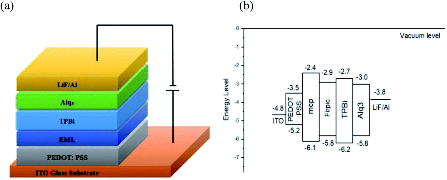 | ||
| Fig. 2 (a) Device structure of the OLEDs and (b) energy level diagram of the OLEDs. | ||
Characterization
The current–voltage–luminance (J–V–L) characteristics and electroluminescence (EL) spectrum of these devices were measured by a test system which consist of computer, Keithley 2410 and SRC-600 spectral radiance colorimeter; transient electroluminescence (TREL) was measured by a transient illuminating test system which consist of a signal generator, a timing controller, a photomultiplier tube and an oscilloscope. The transient photoluminescence (TRPL) was tested using the Horiba Instrument FluoroCube01-N1. All measurements were made under air conditions.3. Results and discussions
Due to the property of high triplet energy level (3.02 eV) and good solubility, mcp is appropriate to be used as the host material for solution-processed blue PhOLED. So firstly in this paper, we chose mcp as the host and Firpic as the dopant to prepare a set of devices with the structure of ITO/PEDOT:PSS/mcp:16 wt% Firpic/TPBi (X nm)/LiF (0.7 nm)/Al (100 nm) by changing the thickness of only one ETL for optimize the electron injection. X is equal to 20 nm, 25 nm, 30 nm, and 35 nm, respectively. The results shows that the luminance and current efficiency of devices increases with the increasing thickness of the ETL, and the turn-on voltage also increases slightly, but the current density of the device decreases as the thickness increases. As shown in Table 1, the Lmax of the device with 35 nm ETL achieves to 5185 cd m−2, while the CEmax achieves to 7.4 cd A−1 and the turn-on voltage is kept at a relatively low level of 3.6 V, which slightly exceeds the best performance of similar devices in ref. 26. As shown in Fig. 1b, the electron injection barrier between TPBi and Al cathode is 1.1 eV, which is too large to inject electron easily and results in electrons accumulation at the TPBi/Al interface. In addition, because the hole mobility (μh ≈ 1.2 × 10⁻⁴ cm2 V−1 s−1) of mcp is much larger than the electron mobility (μe ≈ 5.1 × 10⁻⁶ cm2 V−1 s−1), the majority carrier in the device is hole. Therefore, the device performance depends greatly on the electrons injected to the emission layer. Since the lowest unoccupied molecular orbital (LUMO) of Alq3 is deeper than TPBi, if Alq3 is used as the second electron transport layer, the electron injection barrier can be effectively reduced from 1.1 eV to 0.8 eV.16,27 Therefore, we prepared OLEDs with a additional 10 nm ETL of Alq3, to reduce the electron injection barrier and explore the effect of thickness of TPBi on the device performance.| Devices | Thickness of TPBi (nm) | Turn-on (V) | Lmax (cd m−2) | CEmax (cd A−1) | EQEmax (%) | Color coordinatesa | Peak wavelengthb (nm) |
|---|---|---|---|---|---|---|---|
| a The color coordinates at 1000 cd m−2.b The peak wavelength at 1000 cd m−2. | |||||||
| 1 | 20 | 3.6 | 3158 | 2.1 | 1.0 | (0.15, 0.36) | 471 |
| 2 | 25 | 3.6 | 4043 | 3.6 | 1.7 | (0.15, 0.36) | 472 |
| 3 | 30 | 3.6 | 4857 | 4.9 | 2.3 | (0.15, 0.36) | 471 |
| 4 | 35 | 3.6 | 5185 | 7.4 | 3.3 | (0.16, 0.37) | 472 |
A series of devices with ITO/PEDOT:PSS/mcp:16 wt% Firpic/TPBi (X nm)/Alq3 (0 or 10 nm)/LiF (0.7 nm)/Al (100 nm) structures were fabricated, the thickness X of TPBi is 25 nm, 30 nm, 35 nm, 40 nm and 45 nm, respectively. The turn-on voltage of the double ETL system device is slightly higher as expected, and the brightness and efficiency are improved greatly. It is because that the introduction of Alq3 with a LUMO of 3.0 eV reduces the electron injection barrier and makes it easier for electrons inject into the EML, which helps to balance carriers. And the slightly increasing of turn-on voltage of the device may be due to the interface effect or the increasing thickness of whole EML as shown in Fig. 3a and b. Fig. 3c shows the EL spectrum of different blue OLEDs. All devices exhibit only Firpic emissions centered at 472 nm. As shown in Table 2, the TPBi/Alq3 device achieves a Lmax of 13054 cd m−2 and a CEmax of 11.4 cd A−1, and at the luminance of 1000 cd m−2, the efficiency still maintain at 10.8 cd A−1, which is significantly higher than that of the device with a single ETL of TPBi whose Lmax is 6787 cd m−2 and CEmax is 3.9 cd A−1.
 | ||
| Fig. 3 (a) Current–voltage–luminance (J–V–L) of OLEDs based on different thickness of single and double ETL. (b) Current efficiency of OLEDs based on single and double ETL. (c) Electroluminescence spectra of the blue PhOLEDs. | ||
| Devices | Thickness of TPBi (nm) | Thickness of Alq3 (nm) | Turn-on (V) | Lmax (cd m−2) | CEmax (cd A−1) | EQEmax (%) | Color coordinatesa | Peak wavelengthb (nm) |
|---|---|---|---|---|---|---|---|---|
| a The color coordinates at 1000 cd m−2.b The peak wavelength at 1000 cd m−2. | ||||||||
| 1 | 35 | 0 | 3.6 | 6787 | 3.9 | 1.9 | (0.15, 0.35) | 472 |
| 2 | 25 | 10 | 3.7 | 10187 |
5.9 | 2.8 | (0.15, 0.35) | 471 |
| 3 | 30 | 10 | 3.7 | 10986 |
6.4 | 3.0 | (0.15, 0.35) | 471 |
| 4 | 35 | 10 | 3.8 | 12424 |
8.7 | 4.2 | (0.15, 0.35) | 472 |
| 5 | 40 | 10 | 3.8 | 12346 |
10.6 | 5.0 | (0.15, 0.35) | 473 |
| 6 | 45 | 10 | 4.1 | 13054 |
11.4 | 5.5 | (0.15, 0.35) | 473 |
In order to study the effect of double ETL devices on the electron injection, a group of devices based on holes and electrons were fabricated to analyse the transfer mechanism of carriers.28–30 The devices structure is shown in Table 3. It can be seen from Fig. 4 that the hole current of device 1 is much larger than the electron current of device 2. It means that the electrons and holes inside the EML of the PhOLEDs only with TPBi as the ETL do not match. After introduced Alq3 as the second ETL, the electron current has been much improved greatly in device 3 compared with device 2, which indicates that the introduction of the second electron transport layer Alq3 helps to reduce the electron injection barrier and optimize the carrier balance.
| Devices | Device type | Device structure |
|---|---|---|
| 1 | Hole-only | ITO/PEDOT/mcp:Firpic (16 wt%)/MoO3/LiF/Al |
| 2 | Electron-only | ITO/ZnO/mcp:Firpic (16 wt%)/TPBi/LiF/Al |
| 3 | Electron-only | ITO/ZnO/mcp:Firpic (16 wt%)/TPBi/Alq3/LiF/Al |
 | ||
| Fig. 4 Current density–voltage characteristics in the hole-dominated devices ITO/PEDOT/mcp:Firpic (16 wt%)/MoO3/LiF/Al and the electron-dominated devices ITO/ZnO/mcp:Firpic (16 wt%)/TPBi/LiF/Al and ITO/ZnO/mcp:Firpic (16 wt%)/TPBi/Alq3/LiF/Al. | ||
Through transient electroluminescence measurements, the mechanism of carrier transport, accumulation, capture and even mobility in organic light-emitting devices (OLEDs)31–33 could be analyzed. So we introduced the transient electroluminescence measurement to observe the internal carrier movement of the device and analyze the effect of double ETL. The experimental device of transient electroluminescence measurement and the timing setting of the driving voltage are shown in Fig. 5a. The single ETL device and the double ETL device with the thickness of 35 nm were detected for their transient electroluminescence characteristic curve by applying a voltage pulse with a pulse width of 0.5 ms. The pulse width is sufficient to achieve their steady-state driving. The transient electroluminescence characteristic curve can be seen from Fig. 5b. When a pulse is applied, the double ETL device first reaches its steady-state light emission under the same driven pulse as shown in Fig. 5c, which indicates that the electron injection and transport is improved after the introduction of the second ETL Alq3.
 | ||
| Fig. 5 (a) The experimental device of transient electroluminescence measurement, (b) the transient electroluminescence characteristics and the timing setting of the driving voltage, (c) the transient electroluminescence rising edge characteristic curve, (d) the transient electroluminescence overshoot characteristic curve of the devices based on single and double ETL structure under a periodic electrical pulse of 8 V, 0.5 ms, (e) the PL decay detected in the side of ETL under the excitation of 340 nm of the devices based on single and double ETL structure. | ||
When the bias is turned off, as shown in Fig. 5d, the device is still luminous and exhibits an instantaneous overshoot peak that is stronger than the steady state. The transient overshoot refers to the phenomenon that the luminous intensity suddenly exceeds the steady state a few microsecond after turn off the driving bias, which could be resulted from the recombination of carriers stored in traps or near the interface which accumulated under application of positive bias.32–34 The transient overshoot is strongly dependent, among other parameters, on device materials and structure. Rui Liu et al. reported that the spikes are significantly weaker in devices where a Bphen ETL-HBL layer is added, likely due to enhanced electron transport, and absent in devices where MoO3 replaces CuPc.32 As shown in Fig. 5d, the transient overshoot peak decreases significantly with the addition of the second ETL. From the energy level structure in Fig. 1, the energy barrier between TPBi and the cathode Al reaches 1.1 eV, it is difficult for electrons to jump from the cathode to TPBi and causes a large number of electrons accumulated at the interface. When Alq3 is added, the energy barrier is reduced to 0.8 eV, and the instantaneous overshoot peak is greatly reduced. Therefore, it is concluded that the intensity of the overshoot peak is mainly affected by the electrons stored at the interface. In a single ETL device, when the bias is turned off, the electrons accumulated at the TPBi/cathode interface are released to form excitons with the holes inside the emission layer. These excitons give the overshoot emission and delayed emissions. The addition of the second layer of ETL provides an energy level gradient, which reduces the electron injection barrier and the amount of charge stored at the interface. So the transient overshoot is reduced. The stored charges act as polarons and interact with excitons. The energy could transfer from the triplet exciton to the polaron results in nonradiative recombination. The more charges store in devices, the stronger the interaction between excitons and polarons is. The stronger interaction of exciton–polarons will fast the decay of excitons and reduces the electroluminescence efficiency. Especially under the high current, the stored charges increase greatly, and the efficiency decrease greatly. However, another introduced interface inside the double ETL will results in more defects inside ETL, which attributes more seriously efficiency roll-off in devices. The PL decay of the emission layer with different ETL prove it further.
The emission layer (EML) were fabricated on quartz substrates with the structure of quartz substrate/mcp:Firpic (16 wt%)/ETL (35 nm) were prepared and the PL decay was detected in the side of ETL under the excitation of 340 nm to analyze the effect of an introduced the second ETL layer and the interface on the exciton decay of the emission layer. As shown in Table 4, the distance of the interface between TPBi and Alq3 is different by changing the thickness of TPBi and Alq3. The PL spectra of all films come from the emission of Firpic mainly, as shown as the inset in Fig. 5e. The main PL peak locates at 472 nm corresponding to the exciton recombination of Firpic, and the emission of TPBi was also detected as a tail in the short wavelength. Then the PL decay monitored at 472 nm was detected as shown in Fig. 5e. The PL of Firpic with a single ETL decays faster than that of Firpic with a double ETL. It means that the double ETL is favour to the exciton formation and emit if the exciton zone in the emission layer was considered to be same for different structures. The thicker TPBi is, the more excitation light will be absorbed by TPBi, and the absorption of mcp will decrease, which can be proved by the different PL intensity of TPBi. The results is that the energy transfer from thicker TPBi to Firpic will be weaker because of the long distance from TPBi molecular around its surface to Firpic. The energy transfer probability from the host to Firpic is considered to be same. Therefore, the slower decay of PL with a double ETL will be attributed to the thinner of TPBi which increases the host absorption and the energy transfer probability from TPBi to Firpic. In such case, the number of excitons formed in the emission layer under 340 nm excitation increases along with the thinner of TPBi and reaches the maximum when TPBi is 20 nm. Although the thinner TPBi helps to transfer energy from TPBi to Firpic and increases the number of Firpic excitons, the interface in where there are more defects closes to the emission layer. The interaction between excitons of Firpic and these defects will de-excite nonradiatively the excitons of Firpic. When the thickness of TPBi decreases, the quenching caused by the interface defects is enhanced,35–37 and the PL decay becomes faster again. So it is concluded that the interface is adverse to the exciton emission. Therefore, as shown in Fig. 3b, the efficiency roll-off of devices with a double ETL is more serious than with a single ETL, even the electron injection is improved in devices with double ETL.
| EML | Structure |
|---|---|
| 1 | Quartz substrate/mcp:Firpic (16 wt%)/TPBi (35 nm) |
| 2 | Quartz substrate/mcp:Firpic (16 wt%)/TPBi (25 nm)/Alq3 (10 nm) |
| 3 | Quartz substrate/mcp:Firpic (16 wt%)/TPBi (20 nm)/Alq3 (15 nm) |
| 4 | Quartz substrate/mcp:Firpic (16 wt%)/TPBi (15 nm)/Alq3 (20 nm) |
| 5 | Quartz substrate/mcp:Firpic (16 wt%)/TPBi (10 nm)/Alq3 (25 nm) |
| 6 | Quartz substrate/mcp:Firpic (16 wt%)/TPBi (5 nm)/Alq3 (30 nm) |
4. Conclusions
In summary, compared with the single ETL device, the current efficiency and luminance of the blue phosphorescent device prepared by the solution method of TPBi and Alq3 as a double ETL have been improved. By studying hole-only and electron-only devices, it is found that the addition of Alq3 optimizes the carrier balance. Transient electroluminescence measurement shows that the addition of Alq3 reduces transient overshoot. The results shows that the small spikes of transient overshoot mainly come from the electrons accumulated in the interface between the TPBi and cathode. Therefore, the addition of Alq3 reduces the electron injection barrier and optimizes the device performance to achieve an optimized CEmax to 11.4 cd A−1, Lmax of 13054 cd m−2. At the luminance of 1000 cd m−2, the efficiency still maintain at 10.8 cd A−1, which is significantly higher than that of a single ETL device. The introduced interface in devices with a double ETL has an adverse effect on the exciton emission according to the results of PL decay measurements, which attributes to the serious efficiency roll-off of devices with a double ETL. Hence, it is necessary to optimize the interface effect further in solution-processed PhOLEDs.
Conflicts of interest
There are no conflicts to declare.Acknowledgements
The authors express the thanks to the National Key Research and Development Program of China under Grant No. 2016YFB0401302 and the National Natural Science Foundation of China under Grant No. 61704007 and No. 61775013.References
- C. W. Tang and S. A. VanSlyke, Organic electroluminescent diodes, Appl. Phys. Lett., 1987, 51, 913–915 CrossRef CAS.
- C. W. Tang, S. A. VanSlyke and C. H. Chen, Electroluminescence of doped organic thin films, J. Appl. Phys., 1989, 65, 3610–3616 CrossRef CAS.
- S. Ameen, J. Lee, H. Han, M. Suh and C. Lee, Curing temperature reduction and performance improvement of solution-processable hole-transporting materials for phosphorescent OLEDs by manipulation of cross-linking functionalities and core structures, RSC Adv., 2016, 6, 33212–33220 RSC.
- M. McCarthy, B. Liu, E. Donoghue, I. Kravchenko, D. Kim, F. So and A. Rinzler, Low-Voltage, LowPower, Organic Light-Emitting Transistors for Active Matrix Displays, Science, 2011, 332, 570–573 CrossRef CAS PubMed.
- H. Wu, G. Zhou, J. Zou, C. Ho, W. Wong, W. Yang, J. Peng and Y. Cao, Efficient Polymer White-Light Emitting Devices for Solid-State Lighting, Adv. Mater., 2009, 21, 4181–4184 CrossRef CAS.
- J. Jou, K. Chou, F. Yang, C. Hsieh, S. Kumar, A. Agrawal, S. Chen, T. Li and H. Yu, Pseudo-Natural Light for Displays and Lighting, Adv. Opt. Mater., 2015, 3, 95–102 CrossRef CAS.
- J. Kim, C. Joo, J. Lee, J. Woo, J. Oh, N. Baek, H. Chud and J. Lee, Save energy on OLED lighting by a simple yet powerful technique, RSC Adv., 2015, 5, 8415–8421 RSC.
- E. Kozma, W. Mróz, F. Villafiorita-Monteleone, F. Galeotti, A. Andicsová-Eckstein, M. Catellania and C. Botta, Perylene diimide derivatives as red and deep red-emitters for fully solution processable OLEDs, RSC Adv., 2016, 6, 61175–61179 RSC.
- C. Adachi, M. Baldo and S. R. Forrest, High-efficiency red electrophosphorescence devices, Appl. Phys. Lett., 2001, 78, 1622–1624 CrossRef CAS.
- X. Liu, S. Wang, B. Yao, B. Zhang, C. Ho, W. Wong, Y. Cheng and Z. Xie, New deep-red heteroleptic iridium complex with 3-hexylthiophene for solution-processed organic light-emitting diodes emitting saturated red and high CRI white colors, Org. Electron., 2015, 21, 1–8 CrossRef CAS.
- S. Ye, T. Hu, Z. Zhou, M. Yang, M. Quan, Q. Mei, B. Zhai, Z. Jia, W. Lai and W. Huang, Solution processed single-emission layer white polymer light-emitting diodes with high color quality and high performance from a poly(N-vinyl)carbazole host, Phys. Chem. Chem. Phys., 2015, 17, 8860–8869 RSC.
- N. Chopra, J. Lee, Y. Zheng, S. Eom, J. Xue and F. So, Effect of the charge balance on high-efficiency blue-phosphorescent organic light-emitting diodes, ACS Appl. Mater. Interfaces, 2009, 1, 1169–1172 CrossRef CAS.
- B. Sim, C. Moon, K. Kim and J. Kim, Quantitative Analysis of the Efficiency of OLEDs, ACS Appl. Mater. Interfaces, 2016, 8, 33010–33018 CrossRef CAS PubMed.
- Y. Bai, M. Khan, W. Zhu, X. Jiang and Z. Zhang, A blue organic light emitting diodes with graded junction, Displays, 2008, 29, 365–368 CrossRef.
- X. Zhang, J. Li, M. Khan, L. Zhang, X. Jiang, K. Haq, W. Zhu and Z. Zhang, Improved chromaticity and electron injection in a blue organic light-emitting device by using a dual electron-transport layer with hole-blocking function, Semicond. Sci. Technol., 2009, 24, 075021 CrossRef.
- J. Jang, H. Ji, H. Kim and J. Jeong, TPBI:FIrpic organic light emitting devices with the electron transport layer of Bphen/Alq3, Curr. Appl. Phys., 2011, 11, S251–S254 CrossRef.
- M. Jia, X. Xu, J. Peng, J. Zhang, C. Yao and L. Li, Solution-Processed Double-Layer Electron-Transport Layer for Conventional Blue Phosphorescent Organic Light-Emitting Diodes, Adv. Opt. Mater., 2016, 4, 1635–1641 CrossRef CAS.
- W. Staroske, M. Pfeiffer, K. Leo and M. Hoffmann, Single-Step Triplet-Triplet Annihilation: an Intrinsic Limit for the High Brightness Efficiency of Phosphorescent Organic Light Emitting Diodes, Phys. Rev. Lett., 2007, 98, 197402–197406 CrossRef CAS.
- D. Song, S. Zhao, Y. Luo and H. Aziz, Causes of Efficiency Roll-Of in Phosphorescent Organic Light Emitting Devices: Triplet-triplet Annihilation versus Triplet-Polaron Quenching, Appl. Phys. Lett., 2010, 97, 243304–243307 CrossRef.
- B. Minaev, V. Minaeva and H. Ågren, Theoretical Study of the Cyclometalated Iridium(III) Complexes Used as Chromophores for Organic Light-Emitting Diodes, J. Phys. Chem. A, 2009, 113, 726–735 CrossRef CAS PubMed.
- B. Minaev, G. Baryshnikovb and H. Agren, Principles of phosphorescent organic light emitting devices, Phys. Chem. Chem. Phys., 2014, 16, 1719–1758 RSC.
- G. Baryshnikov, B. Minaev and H. Ågren, Theory and Calculation of the Phosphorescence Phenomenon, Chem. Rev., 2017, 117, 6500–6537 CrossRef CAS PubMed.
- S. Perumal, B. Minaev and H. Ågren, Triplet State Phosphorescence in Tris(8-hydroxyquinoline) Aluminum Light Emitting Diode Materials, J. Phys. Chem. C, 2013, 117, 3446–3455 CrossRef CAS.
- M. Halls and H. Schlegel, Molecular Orbital Study of the First Excited State of the OLED Material Tris(8-hydroxyquinoline)aluminum(III), Chem. Mater., 2001, 13, 2632–2640 CrossRef CAS.
- H. Nakanotani, T. Higuchi, T. Furukawa, K. Masui, K. Morimoto, M. Numata, H. Tanaka, Y. Sagara, T. Yasuda and C. Adachi, High-efficiency organic light-emitting diodes with fluorescent emitters, Nat. Commun., 2014, 5, 4016 CrossRef CAS PubMed.
- J. Jou, W. Wang, S. Chen, J. Shyue, M. Hsu, C. Lin, S. Shen, C. Wang, C. Liu, C. Chen, M. Wud and S. Liu, High-efficiency blue organic light-emitting diodes using a 3,5-di(9H-carbazol-9-yl)tetraphenylsilane host via a solution-process, J. Mater. Chem., 2010, 20, 8411–8416 RSC.
- P. Wei, S. Zhao, Z. Xu, D. Song, B. Qiao, P. Wang and J. Yang, Improved carrier injection and balance in solution-processed blue phosphorescent organic light emitting diodes based on mixed host system and their transient electroluminescence, Synth. Met., 2019, 252, 15–20 CrossRef CAS.
- Y. Zhao, R. Chen, Y. Gao, K. Leck, X. Yang, S. Liu, A. Abiyasa, Y. Divayana, E. Mutlugun, S. Tan, H. Sun, H. Demir and X. Sun, AC-driven, color- and brightness-tunable organic light-emitting diodes constructed from an electron only device, Org. Electron., 2013, 14, 3195–3200 CrossRef CAS.
- A. Kyaw, X. Sun, C. Jiang, G. Lo, D. Zhao and D. Kwong, An inverted organic solar cell employing a sol-gel derived ZnO electron selective layer and thermal evaporated MoO3 hole selective layer, Appl. Phys. Lett., 2008, 93, 221107 CrossRef.
- D. Zhao, X. Sun, C. Jiang, A. Kyaw, G. Lo and D. Kwong, Efficient tandem organic solar cells with an Al/MoO3 intermediate layer, Appl. Phys. Lett., 2008, 93, 083305 CrossRef.
- Y. Luo and H. Aziz, Correlation between triplet triplet annihilation and electroluminescence efficiency in doped fluorescent organic light-emitting devices, Adv. Funct. Mater., 2010, 20, 1285–1293 CrossRef CAS.
- R. Liu, Z. Gan, R. Shinar and J. Shinar, Transient electroluminescence spikes in small molecular organic light-emitting diodes, Phys. Rev. B: Condens. Matter Mater. Phys., 2011, 83, 245302 CrossRef.
- C. Zhang, B. Qiao, S. Zhao, Z. Xu, P. Wang, Y. Chen, F. Yin, G. Teyssedre, C. Laurent and X. Xu, Transient analysis on stored charges in organic light-emitting diodes and their application in alternating current driven electroluminescence, Org. Electron., 2016, 39, 348–353 CrossRef CAS.
- J. Pommerehne, D. Nikolaenkov, V. Nikitenko and H. Bässler, Overshoot effect in transient electroluminescence from single layer organic light-emitting diodes, J. Appl. Phys., 2001, 90, 5554–5560 CrossRef CAS.
- J. Lupton, V. Nikitenko and I. Samuel, Time delayed electroluminescence overshoot in single layer polymer light-emitting diodes due to electrode luminescence quenching, J. Appl. Phys., 2001, 89, 311–317 CrossRef CAS.
- J. Kalinowski, W. Stampor, J. Mężyk, M. Cocchi, D. Virgili, V. Fattori and P. Marco, Quenching effects in organic electrophosphorescence, Phys. Rev. B: Condens. Matter Mater. Phys., 2002, 66, 235321 CrossRef.
- D. Kondakov, J. Sandifer and C. W. Tang, Nonradiative recombination centers and electrical aging of organic light-emitting diodes: direct connection between accumulation of trapped charge and luminance loss, J. Appl. Phys., 2003, 93, 1108–1119 CrossRef CAS.
| This journal is © The Royal Society of Chemistry 2020 |