
 Open Access Article
 This Open Access Article is licensed under a
 Creative Commons Attribution 3.0 Unported Licence
Modification of NiOx hole transport layer for acceleration of charge extraction in inverted perovskite solar cells†
Zezhu Jin,
Yanru Guo,
Shuai Yuan,
Jia-Shang Zhao,
Xiao-Min Liang,
Yujun Qin *,
Jian-Ping Zhang and
Xi-Cheng Ai*
*,
Jian-Ping Zhang and
Xi-Cheng Ai*
Department of Chemistry, Renmin University of China, Beijing 100872, China. E-mail: yjqin@ruc.edu.cn; xcai@ruc.edu.cn
First published on 25th March 2020
Abstract
The modification of the inorganic hole transport layer has been an efficient method for optimizing the performance of inverted perovskite solar cells. In this work, we propose a facile modification of a compact NiOx film with NiOx nanoparticles and explore the effects on the charge carrier dynamic behaviors and photovoltaic performance of inverted perovskite devices. The modification of the NiOx hole transport layer can not only enlarge the surface area and infiltration ability, but also adjust the valence band maximum to well match that of perovskite. The photoluminescence results confirm the acceleration of the charge separation and transport at the NiOx/perovskite interface. The corresponding device possesses better photovoltaic parameters than the device based on control NiOx films. Moreover, the charge carrier transport/recombination dynamics are further systematically investigated by the measurements of time-resolved photoluminescence, transient photovoltage and transient photocurrent. Consequently, the results demonstrate that proper modification of NiOx can significantly enlarge interface area and improve the hole extraction capacity, thus efficiently promoting charge separation and inhibiting charge recombination, which leads to the enhancement of the device performances.
1. Introduction
During the past several years, organic–inorganic metal halide perovskite materials have attracted intensive research in the field of solar cells owing to their strong absorption capacity, excellent defect tolerance, long carrier diffusion length and high carrier mobility.1,2 The power conversion efficiency (PCE) record of perovskite solar cells (PSCs) has increased remarkably from 3.8% in 2009 to 25.2% recently.3,4 The traditional construction of PSCs could be divided into planar and mesoporous structures. In the planar-structured device, a compact TiO2 layer acts as the electron transport layer (ETL) to support the perovskite layer, while there is an additional mesoporous TiO2 (meso-TiO2) layer on the compact TiO2 in the mesoporous PSCs.5,6 The PSCs with meso-TiO2 layer derive from the dye-sensitized solar cells,7 in which the meso-TiO2 could provide the enlarged perovskite/ETL contact area and the photogenerated electrons can be injected from perovskite into ETL very quickly and sufficiently.8,9 In the subsequent development of PSCs, their structures have been varied from conventional configuration (n–i–p) to inverted configuration (p–i–n). Now all the perovskite devices of different structures have been widely explored and demonstrated high photovoltaic performances.10,11 Among these, the inverted PSCs have received increasing attention owing to their advantages of low processing temperature and negligible hysteresis effects.12,13 In inverted PSCs, hole transport layer (HTL) plays an important role in the photovoltaic performances. The appropriate hole transport materials (HTMs) can significantly optimize the Schottky contact, facilitate the interfacial charge separation and reduce the electron–hole recombination.The organic HTMs inherited from conventional configuration have been first used in inverted PSCs owing to the mild fabrication process, while they are limited in the practical application to some extent. For examples, the widely used poly(3,4-ethylenedioxythiophene):poly(styrene-sulfonate) (PEDOT:PSS) and poly[N,N′-bis(4-butylphenyl)-N,N′-bis(phenyl)benzidine] (poly-TPD) suffer from the stability problem caused by the acidic and hygroscopic nature and the high production cost, respectively.14,15 Subsequently, the inorganic materials, including CuSCN,16 CuI17 and nickel oxide (NiOx),18 have been introduced as promising HTM candidates,19 which possess the advantages of low cost, high hole mobility and excellent chemical stability. Particularly, NiOx is an attractive p-type semiconductor HTM with ease of synthesis, high light transmittance and energy level tunability.20 In addition, the doping or modification of NiOx layer can further optimize the surface property, improve the conductivity and modulate the energy level, thereby contributing to the growth of high-quality perovskite films and improving the charge transport capability of HTL.21,22 Recently, inspired by the conventional meso-PSCs, the meso-structure has been adopted in the fabrication of the NiOx HTL of inverted devices. For example, Zhang et al. reported the employment of Zn2+-doped CuGaO2 as HTM scaffold on compact NiOx (c-NiOx) in the inverted PSCs, which obtained significant photovoltaic performance improvement due to the enlarged interfacial contact area and the increased HTL conductivity.23 Han et al. fabricated a hybrid HTL of meso-Al2O3/c-NiOx and improved the photovoltaic performances of the inverted PSC owing to the minimized light absorption loss and interfacial recombination loss.24 Similarly, Alex et al. developed a meso-structure from Cu:NiOx nanoparticle at c-NiOx/perovskite interface which significantly enhanced the hole mobility and the short-circuit current (JSC), as well as decreased series resistance of the HTL.25 Compared with the conventional inverted PSCs based-on NiOx HTL, these works have proposed novel strategy for the modification of NiOx with mesoporous layer and exhibited the advantages of interface optimization, carrier transport improvement and carrier recombination suppression.
In this work, we have developed a facile method to modify NiOx HTL of the inverted PSCs with NiOx nanoparticles (NPs). The increased surface roughness and infiltrating ability of modified NiOx films is beneficial to the growth of high-quality perovskite films. The devices based on the modified NiOx layer demonstrate an impressive photovoltaic behavior improvement owing to the enlarged interface area and the optimized matching of valence band maximum (VBM) of NiOx and perovskite. The charge carrier transport/recombination dynamics of different perovskite films and devices are systematically investigated by the measurements of time-resolved photoluminescence (TRPL), transient photovoltage (TPV) and transient photocurrent (TPC), respectively. Consequently, the results reveal that the modification of NiOx can significantly improve the hole extraction capacity and reduce the charge recombination behaviors, which results in the superior photovoltaic performance of the corresponding device.
2. Experimental
2.1 Fabrication of PSCs
The information of the reagents and chemicals used in this work are provided in the ESI.† Laser-ablated ITO glass was successively rinsed with detergent, deionized water, acetone and ethanol by an ultrasonic bath for 30 min, respectively. Subsequently, the substrate was treated by oxygen plasma for 20 min. For c-NiOx HTL fabrication, NiOx precursor solution (see solution preparation method in ESI†) was spin-coated on ITO substrate at 4000 rpm for 45 s, and then sintered at 300 °C for 1 h in air. The obtained c-NiOx films were used for subsequent devices preparation and film characterization. For the c-NiOx films modified with NiOx NPs, denoted as m-NiOx, NiOx NPs (see synthesis process in ESI†) were spin-coated on the c-NiOx films at 3000 rpm for 30 s, then annealed at 100 °C for 20 min in air.The perovskite active-layer was deposited by a processed method in the nitrogen-filled glovebox. The perovskite ([(FAPbI3)0.85(MAPbBr3)0.15]0.95(CsPbI3)0.05) (FA = formamidine, MA = methylamine) precursor solution was prepared by mixing FAI (1.0 M), PbI2 (1.1 M), MABr (0.2 M), PbBr2 (0.2 M) in anhydrous DMF![[thin space (1/6-em)]](https://www.rsc.org/images/entities/char_2009.gif) :DMSO (DMF = N,N-dimethylformamide, DMSO = dimethyl sulfoxide, 4:1, v:v) mixed solvent, with a slight amount of excessive PbI2.26 After stirring for 1 h, 35 μL of 2.0 M CsI in DMSO was added to the mixed perovskite precursor to achieve the desired triple-cation composition. The solution was spin-coated on the substrates in a two-step program at 1000 and 5000 rpm for 10 and 20 s, respectively. During the second step, 200 μL of chlorobenzene (CB) was poured on the spinning substrate 5 s prior to the end of the program. Then the samples were annealed at 100 °C for 30 min. For PC61BM ([6,6]-phenyl-C61-butyric acid methylester) coating, its solution in CB (20 mg mL−1) was spin-coated at 1500 and 2000 rpm for 6 s and 40 s, respectively, and dried at 80 °C for 20 min. Finally, a 5 nm-thick bathocuproine and a 100 nm-thick Ag counter electrode were deposited by thermal evaporation. The final devices based on c-NiOx and m-NiOx are denoted as “c-PSCs” and “m-PSCs”, respectively.
:DMSO (DMF = N,N-dimethylformamide, DMSO = dimethyl sulfoxide, 4:1, v:v) mixed solvent, with a slight amount of excessive PbI2.26 After stirring for 1 h, 35 μL of 2.0 M CsI in DMSO was added to the mixed perovskite precursor to achieve the desired triple-cation composition. The solution was spin-coated on the substrates in a two-step program at 1000 and 5000 rpm for 10 and 20 s, respectively. During the second step, 200 μL of chlorobenzene (CB) was poured on the spinning substrate 5 s prior to the end of the program. Then the samples were annealed at 100 °C for 30 min. For PC61BM ([6,6]-phenyl-C61-butyric acid methylester) coating, its solution in CB (20 mg mL−1) was spin-coated at 1500 and 2000 rpm for 6 s and 40 s, respectively, and dried at 80 °C for 20 min. Finally, a 5 nm-thick bathocuproine and a 100 nm-thick Ag counter electrode were deposited by thermal evaporation. The final devices based on c-NiOx and m-NiOx are denoted as “c-PSCs” and “m-PSCs”, respectively.
The information of the instruments for the characterization is provided in ESI,† including scanning electron microscopy (SEM), transmission electron microscopy (TEM), atomic force microscopy (AFM), dynamic light scattering (DLS), contact angle (CA), X-ray diffraction (XRD), UV-vis absorption, steady-state photoluminescence (PL) spectroscopy, TRPL, ultraviolet photoelectron spectroscopy (UPS), current density (J)–voltage (V) characteristics and incident photon-to-current efficiency (IPCE) measurement.
2.2 Transient photoelectric experiments
TPV and TPC measurements were conducted following previous report.27 The targeted cell was kept under open-circuit condition and irradiated by a continuous-wave LED laser (520 nm, RGB photonics, Lambda beam) to maintain a steady-state photovoltage (Vph). Then weak laser pulses (532 nm, 7 ns) were applied to induce a small increase (ΔVph) in Vph, with ΔVph/Vph ≤ 5%. Finally, electric signals were recorded by a digital oscilloscope (64 Xs, Lecroy; input impedance, 1 MΩ). A series of desired Vph were obtained by adjusting the intensity of the LED laser through laser power and neutral filters. Corresponding TPC measurement was carried out by immediately switching the input impedance to 50 Ω after TPV measurement. The obtained photovoltage and photocurrent decay traces were fitted by exponential functions, and the charge recombination and transport lifetimes were weighted average values.3. Results and discussion
The modification of c-NiOx is realized through a facile method with the deposition of NiOx NPs, which are obtained by a chemical precipitation method using Ni(NO3)2·6H2O as nickel source (see ESI† for preparation details).28 The as-prepared NiOx NPs are visualized by TEM, as shown in Fig. S1,† which reveals the morphology of the particles aggregated to some extent. The NiOx NPs are further measured with DLS to obtain the size distribution. As depicted in Fig. S2,† the particle size exhibits a relative narrow distribution with an average of about 20 nm. The NPs are also characterized with XRD and the pattern is shown in Fig. S3.† The diffraction peaks at 37.1°, 43.1° and 62.6° can be attributed to the (111), (200) and (220) crystal planes of cubic phase of NiOx.29 The transparency of the c-NiOx and m-NiOx on ITO glass substrate is measured and their optical transmittance spectra are shown in Fig. S4.† Obviously, the introduction of NiOx NPs only leads to a little of transparency decrease and both the samples exhibit good light transmittance (>80%) in the visible region, which insures the light utilization rate of the perovskite layer.30SEM images of the two kinds of HTLs are observed and shown in Fig. 1. Apparently, the films both have excellent coverage, while compared with the smooth surface of c-NiOx (Fig. 1a), the surface of m-NiOx (Fig. 1b) looks much rougher owing to the homogeneously distributed NiOx NPs. The roughness is expected to provide enlarged contact area with the subsequent perovskite layer. The surface topography is further examined by AFM, which reveals that the root-mean-square (RMS) value increases from 5.59 nm of c-NiOx (Fig. 1c) to 8.51 nm of m-NiOx (Fig. 1d) after the deposition of NiOx NPs. The CA test is performed to investigate the infiltrating ability of the different HTLs against the perovskite precursor solution. As exhibited in Fig. S5,† the c-NiOx and m-NiOx substrates display CAs of 15.2° and 8.3°, respectively, indicating that the coating of NiOx NPs layer can help the perovskite solution spread better. The changes of the surface properties of NiOx film upon modification, as will be discussed later, would favor the growth of perovskite film and the optimization of NiOx/perovskite interface.
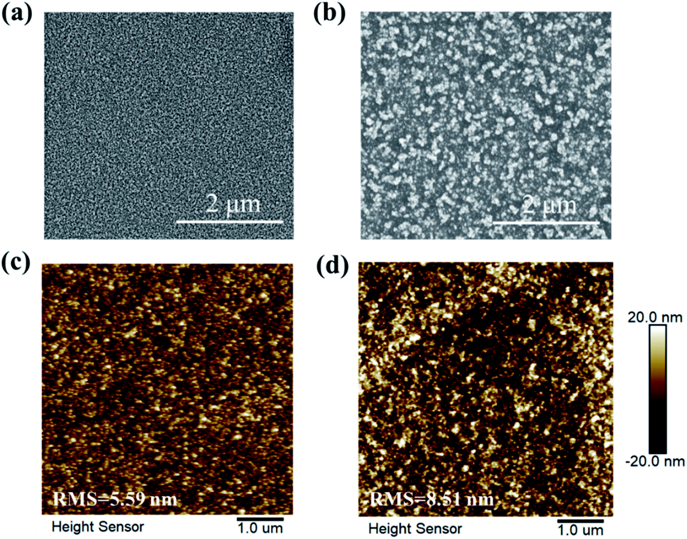 | ||
| Fig. 1 The SEM images of (a) c-NiOx and (b) m-NiOx HTLs. AFM topographic images of (c) c-NiOx and (d) m-NiOx HTLs. | ||
The influence of the different NiOx substrates on the morphology and crystal structures of perovskite films is characterized with SEM and XRD. As shown in Fig. 2, compared with the perovskite film on the c-NiOx (Fig. 2a), the film on m-NiOx presents more smooth and compact morphology (Fig. 2b), which indicates that the modification of substrates could influence the growth of perovskite film. The statistic distributions from the SEM images also displays that the perovskite grains on m-NiOx possess larger average size (245 nm) than those on c-NiOx (230 nm) (Fig. S6†), as well as narrower size distribution. The enlarged perovskite grains with reduced grain boundary can effectively decrease defect density, which would benefit the device performance. XRD patterns of the perovskite films on different NiOx films are illustrated in Fig. 2c, which reveals the typical perovskite characteristics of α black phase rather than δ non-perovskite yellow phase.31 The strong bragg peaks at 13.74°, 19.7°, 24.2°, 28.08°, 31.52° and 40.31° are assigned to the (001), (011), (111), (002), (012) and (022) perovskite crystal planes, respectively, indicating NiOx NPs has no obvious influence on the crystal structures of perovskite under the same preparation conditions of perovskite. In addition, no XRD peaks of residual PbI2 were found in the two samples.32 The UV-vis absorption of the perovskite films on c-NiOx and m-NiOx is also investigated, as shown in Fig. 2d. The improved crystallinity of perovskite on m-NiOx is beneficial to the photon absorption, leading to the gradual rise of the absorption from 750 nm. The absorption ability enhancement of perovskite/m-NiOx would improve JSC of the corresponding device.
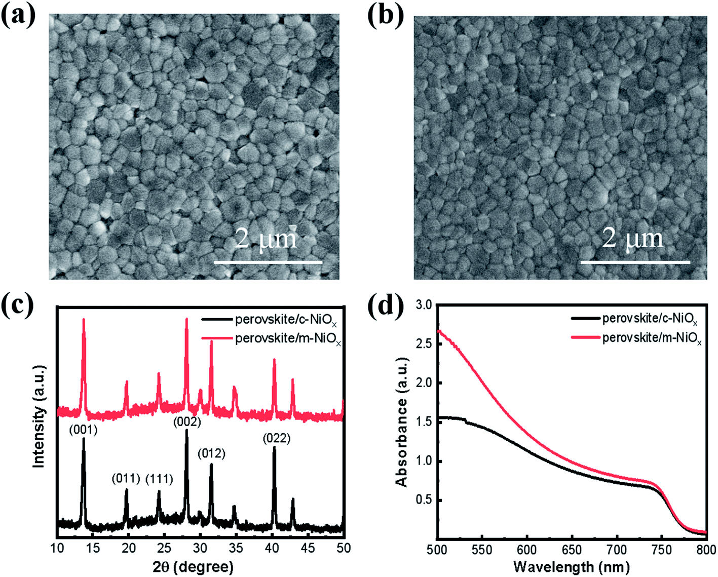 | ||
| Fig. 2 The SEM images of perovskite films based on (a) c-NiOx and (b) m-NiOx HTLs. (c) XRD patterns and (d) absorption spectra of perovskite films deposited on different HTLs. | ||
The Fermi energy (EF) levels of the NiOx films are measured to investigate the influence of NiOx NPs modification. Generally, the EF value of NiOx varies between −4.7 eV and −5.5 eV, depending on its preparation process.33 According to the UPS curves (Fig. S7†), the EF values are −4.79 eV and −4.95 eV for c-NiOx and m-NiOx, respectively, and the VBM of m-NiOx is −5.36 eV, which is slightly lower than −5.22 eV of c-NiOx (see ESI† for calculation details). The value of m-NiOx is much closer to the VBM of the perovskite (−5.60 to −5.40 eV),34–36 which can contribute to the improvement of charge collection and photovoltaic parameters.
To investigate the photogenerated carrier extraction abilities of different HTLs from the perovskite absorber, the steady-state PL spectra and PL decay dynamics are measured, with the perovskite films on quartz as reference. As seen in Fig. 3a, all the perovskite films exhibit the luminescence peaks at about 765 nm, consistent with the band-edge absorption from the UV-vis absorption spectra. Compared with that of perovskite/quartz, the PL emission of perovskite/HTL samples is dramatically quenched owing to the efficient carrier extraction of NiOx. Moreover, the m-NiOx shows a considerably greater PL quenching ability than c-NiOx, implying the promotion of the charge collection and transport efficiency of the former. In details, m-NiOx possesses superior hole extracting ability from the perovskite, which efficiently restricts the PL emission owing to the less recombination of photogenerated electrons and holes in perovskite. The excellent PL quenching ability of m-NiOx results from the enlarged contact area at the perovskite/m-NiOx interface and the optimized energy level alignment with perovskite. As mentioned above, the hole transport from perovskite to m-NiOx is much preferable than to c-NiOx owing to the better matched VBMs of m-NiOx and perovskite. This result is also in agreement with the transient photoelectric experiments (to be discussed in Fig. 5).
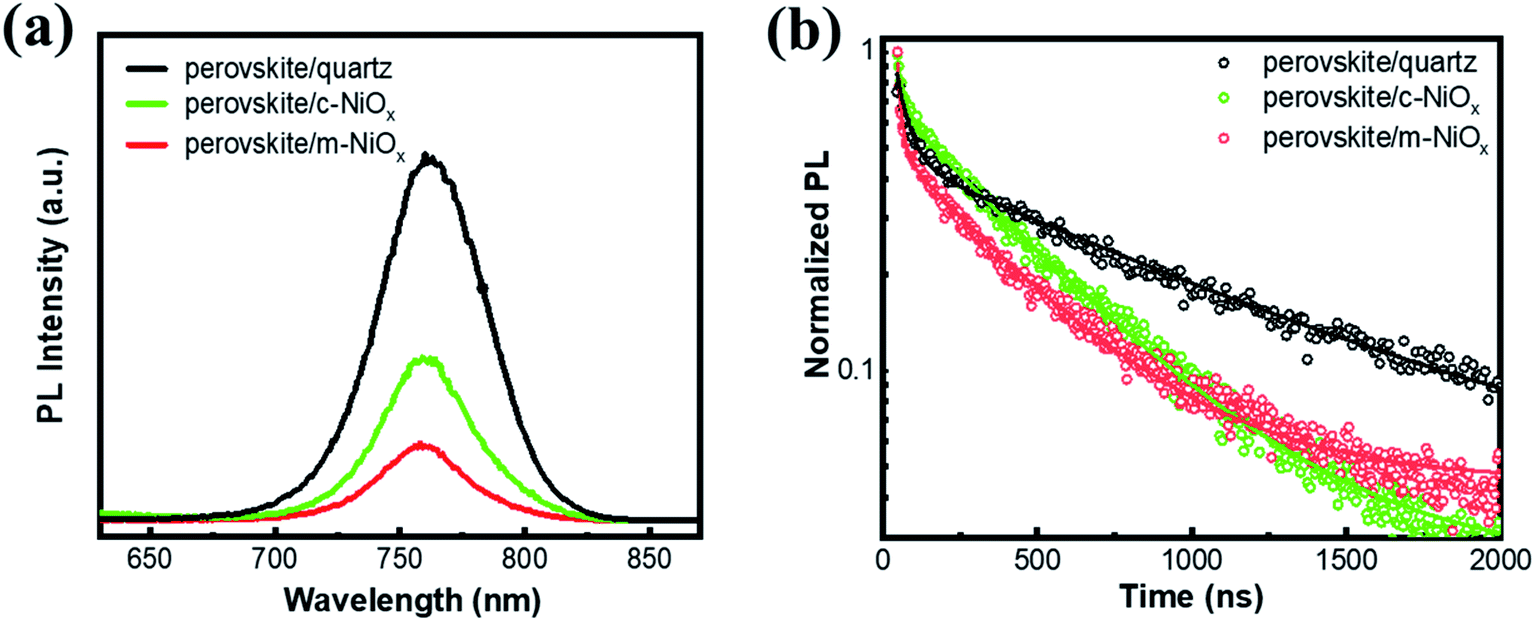 | ||
| Fig. 3 (a) Steady-state PL spectra and (b) PL decay dynamics of perovskite films deposited on different substrates measured at 760 nm. The hollow circles represent experimental data and the solid lines are the fitting results in panel (b). | ||
To further explore the behaviors of the charge carriers in the three perovskite films, the TRPL experiment is conducted and the results are presented in Fig. 3b. The TRPL data are fitted with the biexponential function as below:
| Sample | A1 | τ1 | A2 | τ2 |
|---|---|---|---|---|
| Perovskite/quartz | 0.51 | 40.63 | 0.49 | 943.13 |
| Perovskite/c-NiOx | 0.33 | 22.65 | 0.67 | 421.58 |
| Perovskite/m-NiOx | 0.53 | 13.60 | 0.47 | 385.59 |
The devices based on the two kinds of NiOx as HTLs are fabricated and their photovoltaic performance are compared (the devices based on c-NiOx and m-NiOx are denoted as c-PSCs and m-PSCs, respectively). The cross-sectional SEM images of the two devices are shown in Fig. S8.† Each image clearly demonstrates the distinct layers of the corresponding PSC. Obviously, the HTLs of the device exhibit different thickness with ∼23 nm for c-NiOx and ∼35 nm m-NiOx owing to the modification of the latter with NiOx NPs. It is notable that the thickness of perovskite layer of m-PSC (460 nm) is a little larger than that of c-PSC (440 nm), which could be attributed to the better wettability of m-NiOx for favorable perovskite deposition. The statistical distribution of the photovoltaic parameters of the PSCs is presented in Fig. S9,† which exhibits the superiority of m-PSCs. The J–V curves of the best c-PSC and m-PSC are displayed in Fig. 4a. The c-PSC exhibits PCE of 14.2% with open-circuit voltage (VOC) of 1.01 V, JSC of 20.8 mA cm−2 and fill factor (FF) of 0.67, while the m-PSC demonstrates enhanced performance with PCE of 16.4%, VOC of 1.12 V, JSC of 21.8 mA cm−2 and FF of 0.67. Obviously, the improved PCE of m-PSC is primarily attributable to the increasing JSC and VOC. The increase of JSC of m-PSCs could be ascribed to the enhancement of light absorbance, consistent with the UV-vis absorption (Fig. 2d). The increase of VOC of m-PSCs is mainly due to the reduction of energy loss with m-NiOx as HTL. As mentioned, compared with c-NiOx, the better wettability and rougher surface of m-NiOx could favor the perovskite growth and optimize the perovskite/HTL interface contact, which facilitates the charge transport and reduces the charge recombination. Moreover, the better VBM alignment of m-NiOx with perovskite than that of c-NiOx also benefits the charge extraction from perovskite and injection to HTL. Fig. 4b shows the IPCE spectra for the devices with the corresponding integrated photocurrent densities. The IPCE value correlated to m-PSC exceeds 80%, much higher than that of c-PSC. The higher IPCE means that the m-PSCs has a better utilization of incident light, thus leading to a superior PCE. Meanwhile, the integrated current density is 20.44 and 18.42 mA cm−2 for the two devices, corresponding to the JSC value obtained from the statistical parameters (Fig. S9a†). Considering the similar fabrication conditions, the great improvement in photovoltaic performance of m-PSCs should be ascribed to enlarged charge separation area at the perovskite/HTL interface and the regulation of the energy level of m-NiOx for enhanced charge transport and reduced charge recombination, which is to be proved in the following TPV and TPC results.
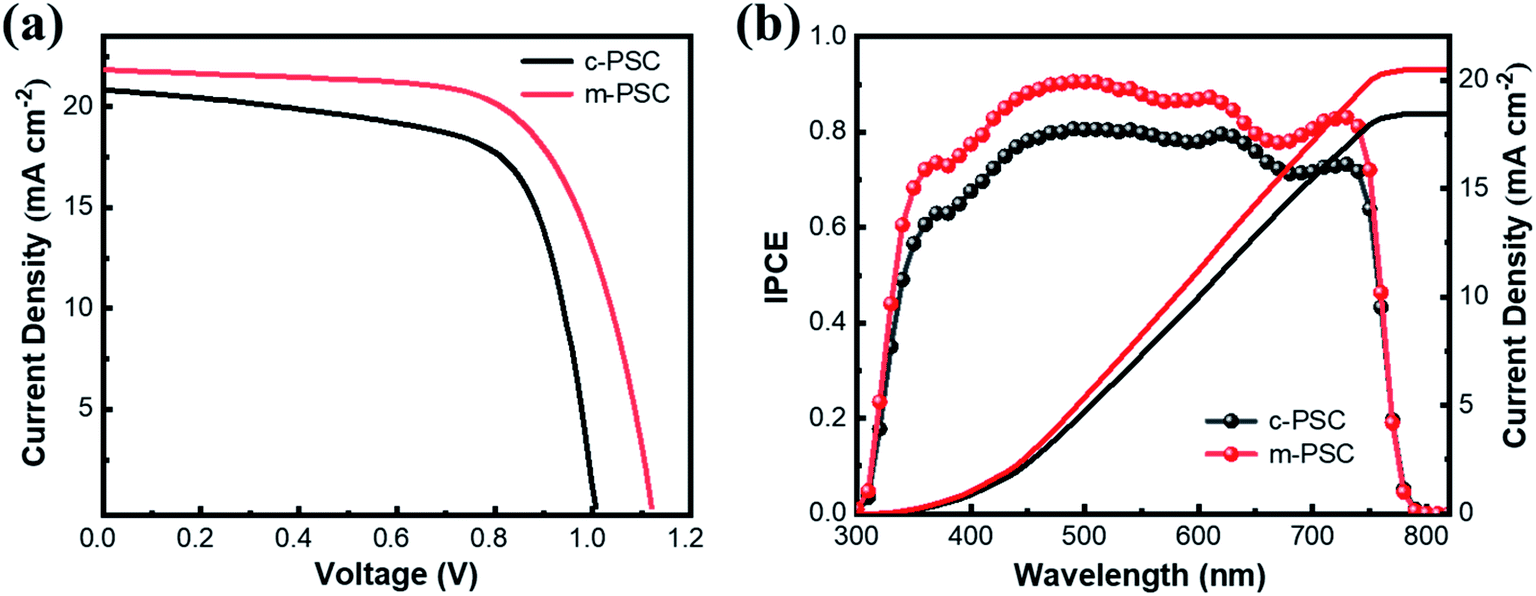 | ||
| Fig. 4 (a) J–V curves and (b) IPCE curves with the corresponding integrated photocurrent of the different HTLs based PSCs. | ||
To probe the origin for photoelectric performance improvement and further unravel the underlying carrier behaviors in the devices, TPV is performed to study the charge recombination dynamics of the targeted PSCs.39,40 Fig. S10† illustrate the corresponding semi-logarithmic plots of normalized Vph decay curves against time for c-PSC and m-PSC, respectively. Apparently, the two devices present distinct decay profiles. Charge recombination lifetimes (τr) are obtained by exponential fitting of the decay traces (see ESI† for fitting details) and Fig. 5a shows the dependence of τr upon different Vph for the two devices. From a rough view, the τr evolution tendency could be divided into two regions with a demarcation point around 550 mV. The τr values are almost constant at 7–8 ms in low voltage region, then τr drops sharply to several μs when the voltage increases from 550 mV to 1000 mV. The two-developing stage of τr along with Vph could be assigned to different competitive recombination processes. In low voltage region, the photogenerated electrons are predominately distributed in deep trap states and the only pathway for a trapped electron/hole to meet or capture another hole/electron is hopping.41 For the two devices with the similar perovskite layer, the effect of NiOx modification on charge separation and transport is negligible in this case,42 thus the almost similar recombination lifetime constants are observed. As the voltage increases continuously, the EF occupied by holes gradually rises and approaches the valence band. Because the population behaviors of electrons and holes are similar, only the behavior of holes is discussed for simplification.43 In this case, it is easy for a trapped hole to accomplish interfacial charge separation driven by the extraction force at perovskite/HTL interface.44,45 The linear correlation between τr and Vph at the semi-logarithmic scale is also observed, which suggests that the charge recombination process should follow the multiple-trap model.46 Compared with c-PSCs, m-PSCs have a longer τr, indicating that the m-NiOx/perovskite interface could promote the charge separation and suppress the charge recombination efficiently. This is mainly attributed to the well matched VBMs of m-NiOx and perovskite, as well as their increased interface contact area.
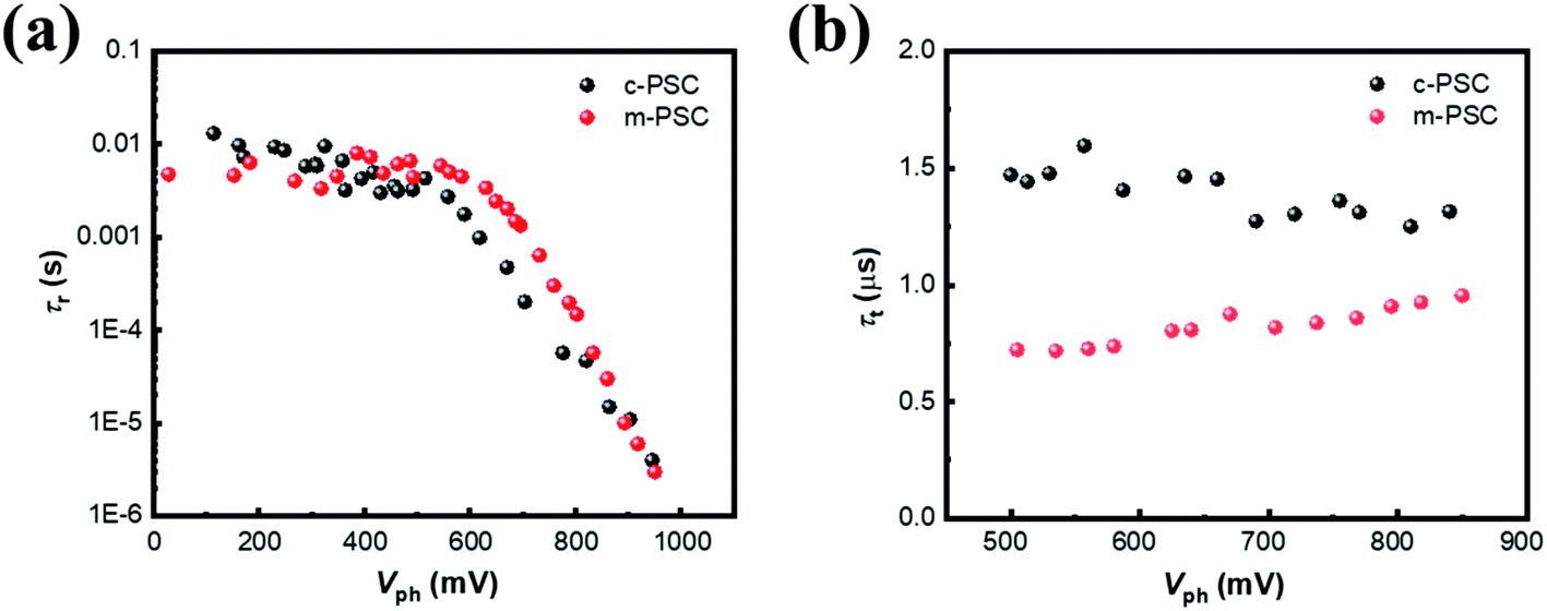 | ||
| Fig. 5 (a) The τr–Vph dependencies from TPV data for different PSCs. (b) The τt–Vph dependencies from TPC data at high voltage (>500 mV) for different PSCs. | ||
Subsequently, TPC measurement is conducted to investigate the charge carrier transport dynamics. Fig. S11† illustrate the corresponding semi-logarithmic plots of normalized photocurrent decay curves against time for different PSCs. Apparently, the devices present similar decay profiles under different Vph. The decay curves are fitted to get the charge transport lifetime (τt) at different voltages with monoexponential decay function as depicted in ESI.† The dependency of τt on Vph from 500 mV to 850 mV obviously exhibits a relatively constant tendency for both devices (Fig. 5b), similar to the previous reports.47,48 The τt values of m-PSC and c-PSC are 0.75 μs and 1.5 μs, respectively, indicating the more efficient charge transport for the former. The results of transient photoelectric experiments quantitatively reveal that the modified HTL behaves superiorly in suppressing charge recombination and elevating charge collection, which accounts for the improvement of the device photovoltaic performance.
4. Conclusions
In summary, a facile method to modify NiOx HTL is proposed by additional deposition of NiOx NPs in inverted planar PSCs. The modification can increase the HTL surface area and infiltrating ability, as well as modulate energy level of NiOx, which is beneficial to the growth of perovskite films and the acceleration of the charge separation and transport. TRPL results exhibits the enhanced charge extraction capability of NiOx HTL owing to the modification. The transient photoelectric tests further reveal that the modification of NiOx can efficiently promote charge transport/separation and reduce the charge recombination, which results in the superior photovoltaic performance of the device. This work could provide new strategies for developing high-efficiency perovskite devices and understanding the underlying charge carrier dynamics.Conflicts of interest
There are no conflicts of interest to declare.Acknowledgements
This work was supported by the National Key R&D Program of China (Grant No. 2018YFA0208701) and the National Natural Science Foundation of China (Grant No. 21773305 and 21973112).References
- K. Schutt, P. K. Nayak, A. J. Ramadan, B. Wenger, Y. H. Lin and H. J. Snaith, Adv. Funct. Mater., 2019, 29, 1900466 CrossRef CAS.
- F. Yu, W. Zhao and S. Liu, RSC Adv., 2019, 9, 884–890 RSC.
- A. Kojima, K. Teshima, Y. Shirai and T. Miyasaka, J. Am. Chem. Soc., 2009, 131, 6050–6051 CrossRef CAS PubMed.
- NREL Best Research-Cell Efficiencies, https://www.nrel.gov/pv/assets/pdfs/pv-efficiency-chart.pdf.
- M. Kim, G. H. Kim, T. K. Lee, I. W. Choi, H. W. Choi, Y. Jo, Y. J. Yoon, J. W. Kim, J. Lee, D. Huh, H. Lee, S. K. Kwak, J. Y. Kim and D. S. Kim, Joule, 2019, 3, 2179–2192 CrossRef CAS.
- H. Min, M. Kim, S. U. Lee, H. Kim, G. Kim, K. Choi, J. H. Lee and S. I. Seok, Science, 2019, 366, 749–753 CrossRef CAS PubMed.
- Y. Wang, H. Y. Wang, J. Han, M. Yu, M.-Y. Hao, Y. Qin, L.-M. Fu, J.-P. Zhang and X.-C. Ai, Energy Technol., 2017, 5, 442–451 CrossRef CAS.
- Y. H. Lv, B. Cai, Y. H. Wu, S. B. Wang, Q. K. Jiang, Q. S. Ma, J. Y. Liu and W. H. Zhang, J. Energy Chem., 2018, 27, 951–956 CrossRef.
- X. Zheng, B. Chen, J. Dai, Y. Fang, Y. Bai, Y. Lin, H. Wei, X. C. Zeng and J. Huang, Nat. Energy, 2017, 2, 17102 CrossRef CAS.
- P. Zhang, J. Wu, T. Zhang, Y. Wang, D. Liu, H. Chen, L. Ji, C. Liu, W. Ahmad, Z. D. Chen and S. Li, Adv. Mater., 2018, 30, 1703737 CrossRef PubMed.
- Y. Lin, L. Shen, J. Dai, Y. Deng, Y. Wu, Y. Bai, X. Zheng, J. Wang, Y. Fang, H. Wei, W. Ma, X. C. Zeng, X. Zhan and J. Huang, Adv. Mater., 2017, 29, 1604545 CrossRef PubMed.
- L. Meng, J. You, T. F. Guo and Y. Yang, Acc. Chem. Res., 2016, 49, 155–165 CrossRef CAS PubMed.
- J. You, L. Meng, T. B. Song, T. F. Guo, Y. M. Yang, W. H. Chang, Z. Hong, H. Chen, H. Zhou, Q. Chen, Y. Liu, N. De Marco and Y. Yang, Nat. Nanotechnol., 2016, 11, 75–81 CrossRef CAS PubMed.
- T. H. Liu, K. Chen, Q. Hu, R. Zhu and Q. H. Gong, Adv. Energy Mater., 2016, 6, 1600457 CrossRef.
- E. Li, Y. Guo, T. Liu, W. Hu, N. Wang, H. He and H. Lin, RSC Adv., 2016, 6, 30978–30985 RSC.
- L. H. Li, J. H. Liang, L. S. Qin, D. Chen and Y. X. Huang, J. Mater. Chem. C, 2019, 7, 6872–6878 RSC.
- J. A. Christians, R. C. Fung and P. V. Kamat, J. Am. Chem. Soc., 2014, 136, 758–764 CrossRef CAS PubMed.
- C. C. Lee, C. I. Chen, C. T. Fang, P. Y. Huang, Y. T. Wu and C. C. Chueh, Adv. Funct. Mater., 2019, 29, 1808625 CrossRef.
- M.-H. Li, P.-S. Shen, K.-C. Wang, T.-F. Guo and P. Chen, J. Mater. Chem. A, 2015, 3, 9011–9019 RSC.
- T. Wang, D. Ding, H. Zheng, X. Wang, J. Wang, H. Liu and W. Shen, Sol. RRL, 2019, 3, 1900045 CrossRef.
- J. Zhang, H. Luo, W. Xie, X. Lin, X. Hou, J. Zhou, S. Huang, W. Ou-Yang, Z. Sun and X. Chen, Nanoscale, 2018, 10, 5617–5625 RSC.
- X. Xia, Y. Jiang, Q. Wan, X. Wang, L. Wang and F. Li, ACS Appl. Mater. Interfaces, 2018, 10, 44501–44510 CrossRef CAS PubMed.
- Y. Chen, X. Jia, Y. Wu, N. Yuan, J. Ding, W.-H. Zhang and S. F. Liu, Nano Energy, 2019, 61, 148–157 CrossRef CAS.
- W. Chen, Y. Z. Wu, J. Liu, C. J. Qin, X. D. Yang, A. Islam, Y. B. Cheng and L. Y. Han, Energy Environ. Sci., 2015, 8, 629–640 RSC.
- K. Yao, F. Li, Q. Q. He, X. F. Wang, Y. H. Jiang, H. T. Huang and A. K. Y. Jen, Nano Energy, 2017, 40, 155–162 CrossRef CAS.
- F. Yang, J. Liu, X. Wang, K. Tanaka, K. Shinokita, Y. Miyauchi, A. Wakamiya and K. Matsuda, ACS Appl. Mater. Interfaces, 2019, 11, 15680–15687 CrossRef CAS PubMed.
- Y. Wang, D. Wu, L.-M. Fu, X.-C. Ai, D. Xu and J.-P. Zhang, ChemPhysChem, 2015, 16, 2253–2259 CrossRef CAS PubMed.
- H. Zhang, J. Cheng, F. Lin, H. He, J. Mao, K. S. Wong, A. K. Jen and W. C. Choy, ACS Nano, 2016, 10, 1503–1511 CrossRef CAS PubMed.
- S. Sajid, A. M. Elseman, H. Huang, J. Ji, S. Y. Dou, H. R. Jiang, X. Liu, D. Wei, P. Cui and M. C. Li, Nano Energy, 2018, 51, 408–424 CrossRef CAS.
- S. Seo, I. J. Park, M. Kim, S. Lee, C. Bae, H. S. Jung, N. G. Park, J. Y. Kim and H. Shin, Nanoscale, 2016, 8, 11403–11412 RSC.
- G. Zheng, C. Zhu, J. Ma, X. Zhang, G. Tang, R. Li, Y. Chen, L. Li, J. Hu, J. Hong, Q. Chen, X. Gao and H. Zhou, Nat. Commun., 2018, 9, 2793 CrossRef PubMed.
- A. A. Zhumekenov, M. I. Saidaminov, M. A. Haque, E. Alarousu, S. P. Sarmah, B. Murali, I. Dursun, X.-H. Miao, A. L. Abdelhady, T. Wu, O. F. Mohammed and O. M. Bakr, ACS Energy Lett., 2016, 1, 32–37 CrossRef CAS.
- B. Mustafa, J. Griffin, A. S. Alsulami, D. G. Lidzey and A. R. Buckley, Appl. Phys. Lett., 2014, 104, 063302 CrossRef.
- Y.-H. Seo, I. H. Cho and S.-I. Na, J. Alloys Compd., 2019, 797, 1018–1024 CrossRef CAS.
- J. Tirado, M. Vásquez-Montoya, C. Roldán-Carmona, M. Ralaiarisoa, N. Koch, M. K. Nazeeruddin and F. Jaramillo, ACS Appl. Energy Mater., 2019, 2, 4890–4899 CrossRef CAS.
- Y. Guo, Z. Jin, S. Yuan, J.-S. Zhao, M.-Y. Hao, Y. Qin, L.-M. Fu, J.-P. Zhang and X.-C. Ai, J. Power Sources, 2020, 452, 227845 CrossRef CAS.
- J.-S. Zhao, H. Y. Wang, M. Yu, M.-Y. Hao, S. Yuan, Y. Qin, L.-M. Fu, J.-P. Zhang and X.-C. Ai, Phys. Chem. Chem. Phys., 2019, 21, 5409–5415 RSC.
- M. Yu, Y. Wang, H.-Y. Wang, J. Han, Y. Qin, J.-P. Zhang and X.-C. Ai, Chem. Phys. Lett., 2016, 662, 257–262 CrossRef CAS.
- Y. Li, Y. Zhao, Q. Chen, Y. M. Yang, Y. Liu, Z. Hong, Z. Liu, Y. T. Hsieh, L. Meng, Y. Li and Y. Yang, J. Am. Chem. Soc., 2015, 137, 15540–15547 CrossRef CAS PubMed.
- J. Xu, A. Buin, A. H. Ip, W. Li, O. Voznyy, R. Comin, M. Yuan, S. Jeon, Z. Ning, J. J. McDowell, P. Kanjanaboos, J. P. Sun, X. Lan, L. N. Quan, D. H. Kim, I. G. Hill, P. Maksymovych and E. H. Sargent, Nat. Commun., 2015, 6, 7081 CrossRef CAS PubMed.
- H. Y. Wang, Y. Wang, M. Yu, J. Han, Z. X. Guo, X.-C. Ai, J.-P. Zhang and Y. Qin, Phys. Chem. Chem. Phys., 2016, 18, 12128–12134 RSC.
- J. Han, H.-Y. Wang, Y. Wang, M. Yu, S. Yuan, P. Sun, Y. Qin, Z.-X. Guo, J.-P. Zhang and X.-C. Ai, RSC Adv., 2016, 6, 112512–112519 RSC.
- M. Yu, H. Y. Wang, M.-Y. Hao, Y. Qin, L.-M. Fu, J.-P. Zhang and X.-C. Ai, Phys. Chem. Chem. Phys., 2017, 19, 19922–19927 RSC.
- J. M. Marin-Beloqui, J. P. Hernandez and E. Palomares, Chem. Commun., 2014, 50, 14566–14569 RSC.
- J. Cui, C. Chen, J. Han, K. Cao, W. Zhang, Y. Shen and M. Wang, Adv. Sci., 2016, 3, 1500312 CrossRef PubMed.
- Y. Wang, D. Wu, L.-M. Fu, X.-C. Ai, D. Xu and J.-P. Zhang, Phys. Chem. Chem. Phys., 2014, 16, 11626–11632 RSC.
- Y. S. Liu, Q. Chen, H. S. Duan, H. P. Zhou, Y. Yang, H. J. Chen, S. Luo, T. B. Song, L. T. Dou, Z. R. Hong and Y. Yang, J. Mater. Chem. A, 2015, 3, 11940–11947 RSC.
- D. Bi, G. Boschloo, S. Schwarzmuller, L. Yang, E. M. Johansson and A. Hagfeldt, Nanoscale, 2013, 5, 11686–11691 RSC.
Footnote |
| † Electronic supplementary information (ESI) available. See DOI: 10.1039/d0ra00209g |
| This journal is © The Royal Society of Chemistry 2020 |