DOI:
10.1039/D0RA00121J
(Paper)
RSC Adv., 2020,
10, 12759-12771
Controlled synthesis of ultrathin MoS2 nanoflowers for highly enhanced NO2 sensing at room temperature†
Received
6th January 2020
, Accepted 24th March 2020
First published on 31st March 2020
Abstract
Fabrication of a high-performance room-temperature (RT) gas sensor is important for the future integration of sensors into smart, portable and Internet-of-Things (IoT)-based devices. Herein, we developed a NO2 gas sensor based on ultrathin MoS2 nanoflowers with high sensitivity at RT. The MoS2 flower-like nanostructures were synthesised via a simple hydrothermal method with different growth times of 24, 36, 48, and 60 h. The synthesised MoS2 nanoflowers were subsequently characterised by scanning electron microscopy, X-ray diffraction, Raman spectroscopy, energy-dispersive X-ray spectroscopy and transmission electron microscopy. The petal-like nanosheets in pure MoS2 agglomerated to form a flower-like structure with Raman vibrational modes at 378 and 403 cm−1 and crystallisation in the hexagonal phase. The specific surface areas of the MoS2 grown at different times were measured by using the Brunauer–Emmett–Teller method. The largest specific surface area of 56.57 m2 g−1 was obtained for the MoS2 nanoflowers grown for 48 h. This sample also possessed the smallest activation energy of 0.08 eV. The gas-sensing characteristics of sensors based on the synthesised MoS2 nanostructures were investigated using oxidising and reducing gases, such as NO2, SO2, H2, CH4, CO and NH3, at different concentrations and at working temperatures ranging from RT to 150 °C. The sensor based on the MoS2 nanoflowers grown for 48 h showed a high gas response of 67.4% and high selectivity to 10 ppm NO2 at RT. This finding can be ascribed to the synergistic effects of largest specific surface area, smallest crystallite size and lowest activation energy of the MoS2-48 h sample among the samples. The sensors also exhibited a relative humidity-independent sensing characteristic at RT and a low detection limit of 84 ppb, thereby allowing their practical application to portable IoT-based devices.
1. Introduction
Gas sensors have attracted considerable attention in the past decades because of their capability to detect toxic and flammable gases and voltaic organic compounds for environmental monitoring, medical diagnosis and human health protection.1,2 For enhanced practical applications, gas sensors are integrated into portable, wearable internet-of-Things (IoT)-based devices.3,4 The gas sensors used in IoT applications must be small for easy integration, have low power consumption and perform well in terms of gas sensitivity, selectivity and stability.5 Among the different types of gas sensors, the ones based on semiconductor metal oxide (SMO) nanostructures are suitable for integration into IoT devices because of their low-cost fabrication, ease of sensing layer synthesis and optimum gas response and sensitivity.6–8 However, these SMO-based sensors work at elevated temperatures, causing high-power consumption and hampering the practical applications of gas sensors in IoT devices. Therefore, the power consumption of gas sensors based on SMO must be reduced to widen their application in portable IoT-based devices. Aside from reducing sensor size using micro-electro-mechanical technologies, new sensing nanomaterials which can operate at room temperature (RT) can also be a promising approach.
Recently, transition metal dichalcogenides such as MoS2 have been considered as a good sensing layer for low-temperature gas sensors because of their high surface-to-volume ratio, distinct semiconducting behaviour, abundant reactive sites for redox reactions and high mobility at RT.9–12 Possessing a layered structure stacked by weak van der Waals interaction, MoS2 has been prepared with different nanostructures by various methods. For example, many groups reported the synthesis of monolayer, bilayer and few-layer MoS2 nanosheets and/or thin film by chemical vapour deposition.13–15 Using the same method, Kumar et al. synthesised nanostructures of vertically aligned MoS2 flakes and nanowire networks.16,17 A previous study also formed MoS2 nanoflakes through sonication-assisted exfoliation.9 Several 3D MoS2 nanostructures, such as spheres and nanosheets, were synthesised using a hydrothermal approach,18–20 which is a simple and low-cost mass-production synthesis method with growth parameters that can be easily controlled. Regarding the sensing characteristics of hydrothermally synthesised MoS2 nanostructures, Zhang et al. fabricated sensors based on MoS2 nanospheres grown via a hydrothermal procedure assisted with CTAB for NO2 detection.21 However, the sensors operate at a high temperature of 100 °C and exhibit a gas response of 60% to a high NO2 concentration of 50 ppm. The MoS2 nanosphere structure synthesised by Yu et al. shows a gas sensitivity of 78% to 50 ppm NO2 at a similarly high temperature of 150 °C.19 In these works, although the operating temperature (OT) of the sensors is lower than that of SMO-based sensors, the sensors work at about 100 °C or 150 °C, causing high power consumption. To further reduce the OT of sensors, Lee et al. fabricated sensors based on surface-activated MoS2 nanosheets with excess sulphur precursor. The sensors work at RT, but their response to a high NO2 concentration of 100 ppm is as low as 99.3%.20 Similarly, sensors based on PbS quantum dot/MoS2 composites show an optimal OT at RT but a low sensitivity of 22.5% to 100 ppm NO2.22 The gas-sensing performance of MoS2 materials is strongly dependent on material morphology and quality, such as specific surface area and crystallite size. Such parameters can be determined by the synthesis method. Thus, a controllable synthesis of MoS2 materials to develop high-performance RT sensors for low concentration of poisonous gases is required for the IoT-based practical application of gas sensors.
This study reported the controlled synthesis of pristine MoS2 nanoflowers with different growth times of 24, 36, 48 and 60 h by using a simple hydrothermal method that does not require further processes, such as surface functionalisation, decoration and/or doping. The synthesised MoS2 nanostructures having the largest specific surface area and the smallest crystallite size showed excellent gas-sensing characteristics at RT to low NO2 concentrations of 1–10 ppm. The gas response of the sensor based on the synthesised MoS2 to a low NO2 concentration of 10 ppm at RT was as high as 67.4%. The fabricated sensors showed a low detection limit (DL), good selectivity to interfering gases and humidity-independent sensing characteristics at RT, which are crucial for their practical application to portable IoT-based devices.
2. Experimental
2.1 Preparation of MoS2 nanoflower-like structures
MoS2 nanoflower-like nanostructures were grown via a facile hydrothermal method, as shown in Fig. 1. Firstly, 0.617 g of ammonium molybdate [(NH4)6Mo7O24·4H2O 99.98% purity, Sigma-Aldrich], 0.79 g of thiourea (CH4N2S, ≥99% purity, Sigma-Aldrich), and 0.69 g of hydroxylammonium chloride (NH2OH·HCl, 98% purity, Sigma-Aldrich) were dissolved in 80 mL of deionised (DI) water. This solution was poured into a 100 mL Teflon autoclave and then heated to 200 °C as described in our previous work.23 The samples were stored at different times of 24, 36, 48 and 60 h and hereafter called MoS2-24 h, MoS2-36 h, MoS2-48 h and MoS2-60 h, respectively. Afterwards, the growth solution was cooled down to RT, centrifuged at 4000 rpm to obtain the precipitated powder, which was washed by DI water and ethanol, and finally dried at 60 °C for 24 h. The morphological, crystal, and vibrational properties of the obtained MoS2 nanostructures were characterised by field-emission scanning electron microscopy (FESEM, JEOL JSM-7600F), X-ray diffraction (XRD, Advance D8, Bruker) and Raman spectroscopy (Renishaw, InVia confocal micro-Raman). The composition, atomic structure and specific surface area of the synthesised nanostructures were also investigated using energy-dispersive X-ray spectroscopy (EDX, detector integrated in the FESEM system), high-resolution transmission electron microscopy (TEM Tecnai G2 20S-TWIN/FEI) and Brunauer–Emmett–Teller (BET; Micromeritics' Gemini VII) method, respectively.
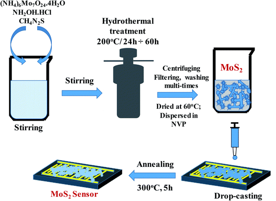 |
| | Fig. 1 Experiment procedure for the controlled hydrothermal synthesis of MoS2 nanoflowers and drop-casting fabrication of the MoS2 sensor. | |
2.2 Fabrication of MoS2 nanoflower-based sensors
MoS2 nanostructure-based gas sensors were fabricated using a drop-casting technique as previously described.24 The synthesised MoS2 nanostructures were dispersed in the N-vinyl-pyrrolidone solvent using an ultrasonic bath. The dispersed solution was coated on the interdigitated Pt electrodes via the drop-casting method, as shown in Fig. 1. The sensors based on the MoS2 nanostructures were heated to 300 °C and placed in vacuum for 5 h to remove the binder and to intensify the contact between the synthesised MoS2 nanostructures and Pt electrodes. The gas-sensing characteristics of the synthesised nanostructures based on the change in the resistance of the sensors with and without exposure to analytical gases were characterized and collected by using a Keithley system (model no. 2602). The setup for gas-sensing measurement is illustrated in Fig. S1,† in which three mass flower controllers (MFCs) were employed for gas mixing. The desired gas concentration (C(ppm)) was calculated as follows:| |
 | (1) |
where C0 is concentration of standard gas used in the measurement, f and F are the flow rates of the standard gas and compressed air in standard cubic centimetre per minute (sccm), respectively. MFC-1 controlled the flow rate of the analytical gas; MFC-2 controlled the flow rate of the press air, which was mixed with the standard gas; and MFC-3 controlled the baseline air flow, which has the same flow rate as the total flow rate of MFC-1 and MFC-2 (Fig. S1†). Details about the gas-sensing measurement setup can be found elsewhere.25,26 In the current work, the total gas flow rate was set to 400 sccm, and the standard NO2 gas with concentration of 100 ppm balanced in nitrogen was used. To obtain the desired NO2 concentrations, we mixed the NO2 standard gas with press air using MFC-1 and MFC-2 with different flow rates (Table. S1†). A gas of desired concentration was flown onto the sensor surface. Two tungsten needles were contacted on the sensor electrodes to transmit electrical signals to a Keithley sourcemetre (model no. 2602) to obtain the resistance response curves. The gas response (S) in percentage was defined as follows:| |
 | (2) |
where Rair and Rgas are the sensor resistance in dry air and in the presence of the test gas, respectively. The selectivity of the sensors was tested with other interfering gases, such as NH3, CO, H2 and CH4.
3. Results and discussion
The surface morphological properties of the synthesised nanostructures were characterised by FESEM. Fig. 2 shows low- and high-magnification SEM images of the MoS2 nanostructures grown at different times of 24 [Fig. 2(a) and (b)], 36 [Fig. 2(c) and (d)], 48 [Fig. 2(e) and (f)], and 60 h [Fig. 2(g) and (h)]. The nanostructures comprised many petal-like nanosheets agglomerated together to form flower-like nanostructures. The low-magnification SEM images illustrated a dissociation of bunches of flower-like nanostructures when the growth time was prolonged from 24 h to 60 h. The thin petals of the flower-like nanostructures were responsible for improving gas sensor performance. The samples grown at different times were difficult to distinguish in the SEM images, as shown in detail in the following.
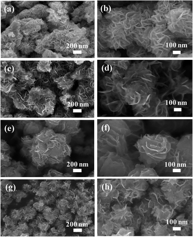 |
| | Fig. 2 SEM images of MoS2 nanoflowers synthesised at different growth times: (a and b) at 24 h, (c and d) at 36 h, (e and f) at 48 h, (g and h) at 60 h. | |
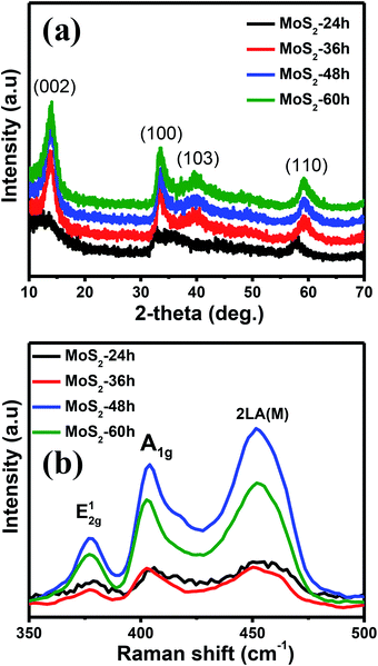
Fig. 3(a) and (b) reveal the XRD patterns and Raman spectroscopy of the MoS2-24 h, -36h, -48h, and -60h samples to investigate the crystal structure properties of the synthesised MoS2 flower-like nanostructures with different growth times. Aside from the XRD pattern of the MoS2 grown for 24 h, those of the rest showed pronounced peaks located at 2θ = 13.76°, 33.36°, 39.87° and 59.40°, which are indexed to the (002), (100), (103) and (110) planes of the hexagonal phase of MoS2, respectively (JCPDS-37-1492).27 The data showed that the diffraction peaks became higher and sharper with prolonged growth time, indicating an improvement of the crystallinity and the formation of the well-stacked layered structure of the MoS2 flower-like nanostructure along the c-axis.28 The crystallite size of the MoS2 nanostructures synthesised with different growth times was calculated using the Scherrer formula:
| |
 | (3) |
where
D,
λ,
β and
θ are the crystallite size, X-ray wavelength (0.154 nm), full width at half maximum and Bragg angle of the XRD peaks, respectively. For comparison purpose, we used the (110) peak of the XRD patterns of the four samples. The crystallite sizes of 4.43, 3.84, 3.51 and 3.67 nm corresponded to the MoS
2-24 h, -36 h, -48 h and -60 h samples. The MoS
2 sample grown for 48 h had the smallest crystallite size, which contributed to the enhancement of gas-sensing properties.
 |
| | Fig. 3 (a) XRD patterns and (b) Raman spectra of MoS2 nanoflowers synthesised at different growth times. | |
Resonant Raman (RR) spectroscopy with a laser wavelength of 633 nm was used to investigate the atomic vibrational modes of the MoS2 flower-like nanostructures grown at different times. Fig. 3(b) shows the Raman spectra of the MoS2 flower-like nanostructures grown for 24, 36, 48 and 60 h. All spectra revealed three Raman vibrational modes located at approximately 378, 403 and 452 cm−1. The first two peaks indexed as E12g and A1g arose from the in-plane and out-of-plane vibrational modes of the hexagonal MoS2 between Mo and S and S and S, respectively.29 The frequency difference between two active modes of all the samples, which is a fingerprint to estimate the thickness of the MoS2 nanosheets, was rather similar. Thus, changes in the nanosheet thickness of the MoS2 grown at different times were difficult to discern. The intensity of the A1g mode was much higher than that of the E12g peak, which can be attributed to the spectra in the resonant condition of the MoS2 flower-like nanostructures.30,31 Under this condition, the direct transition with the final electronic state at K point is associated with dz2 orbitals of the Mo atoms.30 These are aligned in the vibrational direction of S atoms (A1g mode), resulting in strong electron–phonon coupling along the direction of the A1g mode. Thus, the enhancement of the A1g peak intensity with respect to the E12g peak occurred under RR spectroscopic conditions.30 The third peak at 452 cm−1 in the RR spectra of the MoS2 nanostructures was associated with the second-order longitudinal acoustic phonons (2LA(M) mode) at the M point.
To further investigate the atomic structure of the MoS2 flower-like nanostructures, we performed TEM measurements on the synthesised samples using Tecnai G2 20S-TWIN/FEI TEM with a thermal LaB6 electron gun at 200 kV offering a point resolution of 0.24 nm and lattice resolution of 0.144 nm. The MoS2 nanoflower material for measurement was prepared by dissolving a small amount of MoS2 nanoflowers into the ethanol solvent. A small drop of the solution was put onto the TEM specimen (copper grid with carbon foil) by using a micro pipette. Fig. 4(a) and (b) reveal representative TEM images of the MoS2 nanoflower grown for 48 h. The low-magnification TEM image, as shown in Fig. 4(a), indicates that the flower-like nanostructures were composed of curved ultra-thin nanosheets. The width of the uneven sheets was about several hundred nanometres. The high-resolution TEM image of the MoS2 nanostructures (Fig. 4(b)) reveals that the lattice fringes of the MoS2 were also curved but still clearly visible, thereby confirming the formation of the well-defined crystal structure of MoS2. The lattice fringe spacing was 0.63 nm, which was assigned to the (002) crystal plane of the MoS2 flower-like nanostructures. This result is in agreement with previous results.32 The compositional properties of the synthesised MoS2 flower-like nanostructures were investigated using EDX. Fig. 4(c) exhibits a representative EDX spectrum of the MoS2 nanoflowers grown for 48 h. In the measured energy range, the Kα and Lβ fluorescence lines of S and Mo were very close, respectively. Thus, deconvolution of the broad peak in the energy ranging from 2 keV to 2.6 keV of the EDX spectrum was performed. The result clearly showed the presence of S and Mo in the spectrum, which were generated in the synthesised flower-like nanostructures.
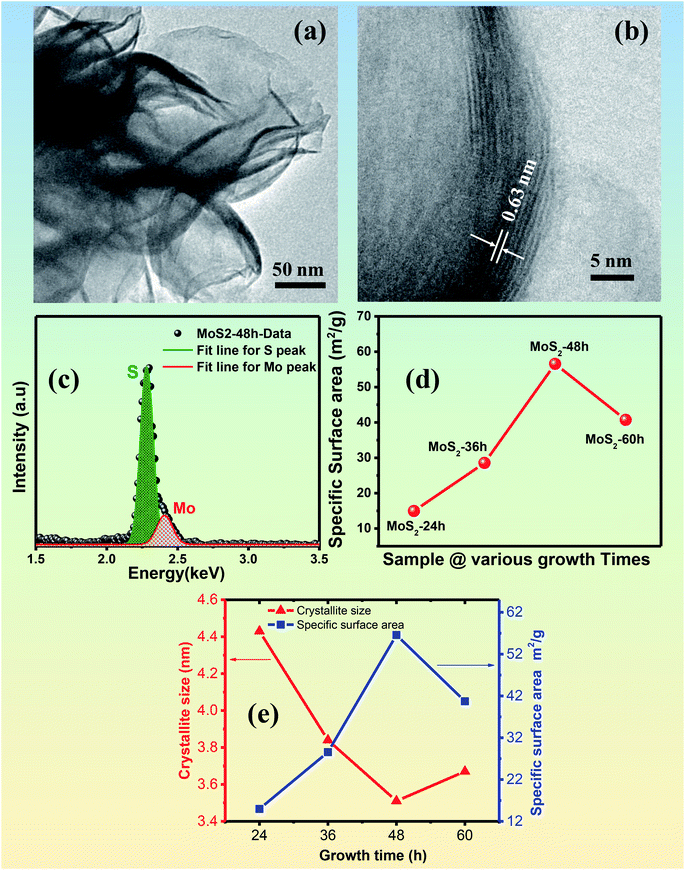 |
| | Fig. 4 (a and b) are representative low- and high-magnification TEM images. (c) EDS analysis of MoS2 with the growth time of 48 h. (d) BET specific surface area of MoS2 nanoflowers synthesised at different growth times. (e) Correlation between the crystallite size and specific surface area of the MoS2 nanostructures synthesised with different growth times. | |
The specific surface area, one of the key parameters responsible for the high gas-sensing performance of the synthesised nanostructures was measured using the BET method by N2 adsorption isotherm at the relative pressure (P/Po) range of 0.05–0.3. The N2 adsorption quantities of the synthesised MoS2 nanostructures under four growth times as a function of relative pressure are shown in the ESI [Fig. S2(a)–(d)].† The BET specific surface areas of the four samples were calculated, as shown in Fig. 4(d). The specific surface area of the synthesised MoS2 nanostructures increased from 14.97 m2 g−1 to 56.57 m2 g−1 with prolonged growth time from 24 h to 48 h, respectively. When the growth time was further prolonged to 60 h, the BET specific surface area of the synthesised MoS2 nanostructures was reduced to 40.72 m2 g−1. The highest specific surface area was reached at 48 h growth time. The results are consistent with the above-mentioned XRD data of the MoS2 nanostructures. For a detailed comparison, Fig. 4(e) represents the correlation between the crystallite size and the specific surface area of the MoS2 synthesised with different growth times of 24, 36, 48 and 60 h. The graph indicates a strong correlation between the two parameters. The smaller crystallite size resulted in the larger specific surface area of the synthesised MoS2, which is in agreement with the theoretical relation between the two parameters (SBET ∼ constant/D, where SBET is the specific surface area and D is the crystallite size).33 The data confirm the largest specific surface area and smallest crystallite size obtained for the MoS2 synthesised with a growth time of 48 h Thus, this sample was expected to show the highest gas response among the different samples. The optimal experiment condition wherein the largest specific surface area and smallest crystallite size of the sample were reached for the growth of MoS2 nanostructures plays an important role in the development of a high-performance gas sensor based on MoS2 nanostructures.25
Prior to the gas-sensing measurements of the sensors based on the MoS2 nanostructures grown at different growth times, the current (I)–voltage (V) characteristics of the sensors were acquired in air with an applied bias voltage from −5 V to 5 V and temperature ranging from RT to 150 °C (data not shown). The current increased with increasing temperature, thereby indicating the semiconducting characteristic of the synthesised MoS2 nanostructures. The interface between the sensing layer and the Pt electrode showed a non-ohmic contact possibly because of the formation of the homojunction of the MoS2 nanoflowers.
The sensing layer with smaller activation energy has been demonstrated showing higher gas sensitivity of the sensor.34,35 The activation energy (Ea) of the MoS2 flower-like nanostructures can be calculated through the temperature-dependent conductivity as expressed by the Arrhenius eqn (4) as follows:34
| |
 | (4) |
where
I is the current of the MoS
2 flower-like nanostructures,
kB is the Boltzmann constant (≈8.62 × 10
−5 eV K
−1) and
T is the absolute temperature. Using the Arrhenius equation and at an applied bias voltage (
i.e. 5 V), we plotted ln(
I) as a function of 1/
T for four MoS
2 samples grown at different times, as shown in
Fig. 5. The activation energy was calculated from the slope of the Arrhenius plot through a linear fitting of ln(
I) with respect to 1/
T. The calculated results showed that the activation energy of the MoS
2-48 h sample was about 0.08 eV, which is the smallest among the
Ea of the other samples. Thus, in combination with the largest specific surface area of the MoS
2 nanostructures grown for 48 h among four samples, the sensor based on the MoS
2-48 h sample was expected to have the highest sensitivity.
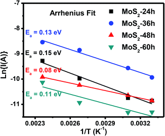 |
| | Fig. 5 Arrhenius fit of the ln(I(A)) versus 1/T of the MoS2 nanostructures grown for 24, 36, 48 and 60 h. | |
Fig. 6(a) exhibits the transient resistance of the sensor to 1–10 ppm NO2 on the basis of the MoS2 flower-like nanostructures grown for 48 h at RT, 50 °C, 100 °C and 150 °C. The data showed that the baseline resistance of the sensor based on the MoS2 nanoflowers decreased when the OT was increased from RT to 150 °C, indicating the semiconducting characteristics of the synthesised MoS2. When the sensor was exposed to NO2 as an oxidising gas, the sensor resistance decreased, thereby showing p-type semiconducting behaviour. Fig. 6(b) reveals the sensor response in percent as a function of NO2 concentration at different OTs. The response of the sensor increased with increasing NO2 gas concentration from 1 ppm to 10 ppm. High amount to gas molecules contributes to absorption, and reaction increases gas sensitivity. The sensor exhibited the highest performance at RT within the measured temperature range, which can be attributed to large various active sites for gas adsorption at RT.2 Namely, the number of defects such as S vacancies was significantly high in the MoS2 at RT. It was about 5% as reported elsewhere for an identical system.9 These defects serve as reactive sites with the target gas, thereby increasing gas response at RT.19 When the working temperature of the MoS2 sensor was increased, the number of defects decreased, which reduced the number of reactive sites. Thus, the gas response decreased at higher temperatures.
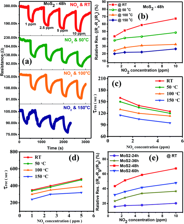 |
| | Fig. 6 (a) Transient resistances of the sensor based on the MoS2-48h sample to 1–10 ppm NO2 at RT, 50 °C, 100 °C and 150 °C. (b) Gas response as a function of the NO2 concentrations at various temperatures. (c and d) are response and recovery times of the MoS2-48h senor as a function of NO2 concentrations at different temperatures. (e) Comparison of the gas responses to 1–10 ppm NO2 of the sensors based on MoS2 grown for 24, 36, 48 and 60 hat RT. | |
Normally, the defect-dominated process on the surface of MoS2 contributes to the significant response and recovery times because of the high adsorption energy of the target gas with the defects as reactive sites.36 Previous works reported that sensors based on pristine MoS2 of different nanostructures have incomplete recovery at RT possibly because of the high adsorption energy of NO2 on the MoS2 surface or the strong binding between NO2 and the reactive sites of MoS2.17,37 However, some other works indicated that in spite of slow rates of gas adsorption and desorption, the pristine MoS2-based sensors showed the complete recovery at RT to target gases.20,38–40 This characteristic can be attributed to several factors, such as high specific surface area, defective/strained surface and weak van der Waals binding between the target gas and the MoS2 surface.20,38,39 In addition, Ikram et al. indicated that the high specific surface area not only increases the response of the sensor but also plays an important role in fast response and recovery times.41 Thus, understanding the detailed mechanism for the complete recovery of the sensor is still under debate because of the combined effects of physi-, chemi-sorption, role of defects sites and transduction mechanism37. As shown in Fig. 6(a), despite its slow rates, the sensor based on MoS2-48 h MoS2 showed complete response and recovery to NO2 gas at RT. This result can be mainly attributed to the large specific surface areas and the defects on the MoS2 surface.
For quantitative analysis, the response and recovery times of the MoS2-48 h MoS2 sensor to 1–5 ppm NO2 (no calculation at 10 ppm NO2 because the recovery resistance curves were not measured completely at this concentration) were deduced from its transient resistance, as shown in Fig. 6(c) and (d), respectively. The data showed that the response time of the sensor working below 100 °C was not much different. A similar behaviour was also obtained for the recovery time of the sensor at low temperatures. While the sensors working at high temperatures of 100 °C and 150 °C showed evidently faster response and recovery times than that working at low temperatures. The response/recovery times to 5 ppm NO2 were about 125 s/485 s and 95 s/320 s at RT and 150 °C, respectively. The fast response/recovery times can be attributed to the thermal energy generated at high temperatures, which reduced the defects on the MoS2 surface and accelerated the desorption of the absorbed gas.
The transient resistance curves of the sensors based on MoS2 grown for 24, 36, and 60 h to 1–10 ppm NO2 gas at different temperatures are shown in Fig. S3, S4 and S5† (in complementary data), respectively. The data also indicated the p-type semiconducting characteristic of the synthesised MoS2 under different growth times. The gas responses of each sensor are summarised in Fig. S3–S5.† Fig. 6(e) presents a comparison of the NO2 gas responses of the sensors based on the MoS2 grown for 24, 36, 48 and 60 h at RT. Among the sensors, the sensor based on the MoS2-48 h sample had the highest response to 1–10 ppm NO2. The highest gas response at 10 ppm NO2 was 67.4%. The highest sensitivity can be attributed to the synergistic factors of the largest specific surface area, smallest crystallite size and lowest activation energy of the MoS2-48 h sample as presented above, thereby contributing to the improved sensitivity of the sensor. For all the measured sensors, high gas response was obtained for the low activation energy, small crystallite size and large specific surface area of the MoS2 sensing layer. Namely, the gas sensitivity gradually decreased for the sensors based on MoS2 nanostructures grown for 48, 60, 36 and 24 h, which is consistent with their reduced specific surface area (56.57, 40.72, 28.55 and 14.97 m2 g−1), increased activation energy (0.08, 0.11, 0.13 and 0.15 eV) and crystallite size (3.51, 3.67, 3.81 and 4.43 nm).
The gas-sensing characteristics of the MoS2 nanostructures can be explained by the Langmuir–Hinshelwood mechanism for chemical reaction of the tested gas with adsorbed oxygen molecules on the surface of the sensing layer, leading to change in the sensor's resistance.36,42,43 As shown in Fig. 7(a), when the p-type semiconducting MoS2 nanostructures were exposed to ambient air, oxygen molecules were adsorbed on the MoS2 surface and electrons were captured from the valence band of the MoS2 to form the oxygen ion species (O2−, O− and O2−) (eqn (5)–(8)) as follows:
| | |
O2(ads) + 4e− → 2O2−.
| (8) |
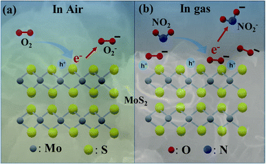 |
| | Fig. 7 NO2 sensing mechanism of the MoS2 nanoflowers: (a) in air and (b) in tested gas. | |
However, the sensors were measured at low temperature from RT to 150 °C; thus, the oxygen ion O2− was dominant.44,45 The adsorption of oxygen molecules on the surface of the p-type MoS2 by trapped electrons from the valence band resulted in a hole accumulation layer and decreased baseline resistance. When the NO2 was injected into the sensing layer, as illustrated in Fig. 7(b), the oxidising gas extracted electrons, which reacted with the adsorbed oxygen followed by, eqn (9) and (10) thereby creating more holes into the valence band.46 Therefore, the sensor resistance decreased upon exposure to NO2 gas, as follows:19,46
| | |
NO2 + O2− + 2e− → NO2− + 2O−,
| (10) |
| | |
NO2− + VS++ → NO2 + h+.
| (11) |
A large number of defects such as S vacancies (VS++) at RT can be found in pristine MoS2, and these defects serve as reactive sites for target gas adsorption.19,36 The interaction mechanism between NO2 gas molecules and S vacancies is shown in, eqn (9) and (11) which generated significant holes into the valence band, thereby highly increasing the gas response at RT. When the temperature was increased, the electron mobility increased but the number of electrons may not be increased significantly; inversely, the number of S vacancies decreased drastically. As a result, less holes were created, and the response decreased at high temperatures.
Recent works on NO2 sensors based on different MoS2 nanostructures are summarised in Table 1 in terms of OT, gas concentration and gas response. The sensors based on pure MoS2 nanostructures showed very low response to NO2 gas even at high concentrations (5–500 ppm) under RT and elevated OT. The gas response of the sensors was increased by the surface functionalisation and heterojunction formation of the MoS2 nanostructures with other noble metals and metal oxide/carbon nanotubes, respectively. However, the enhancement of the response was still negligible and the NO2 gas concentration was extremely high (50–100 ppm). For example, Deokar et al. reported that a sensor based on MoS2–carbon nanotube hybrids exhibits a response of 12.6% to 50 ppm NO2 at RT.47 In the present study, the pure MoS2 flower nanostructure-based sensor showed a high response of 67.4% to a low NO2 concentration of 10 ppm under similar OT at RT.
Table 1 NO2 gas-sensing performance of the sensors based on different MoS2 nanostructures
| No. |
Materials |
OT (°C) |
Concentration (ppm) |
Responsea (%) |
Ref. |
Response was calculated by  ; or ; or  |
| 1 |
MoS2 nanowire network |
60 |
5 |
18.1 |
17 |
| 2 |
MoS2 nanospheres |
100 |
50 |
60 |
21 |
| 3 |
MoS2–Au thin film |
RT |
2.5 |
30 |
55 |
| 4 |
MoS2/Si heterojunctions |
RT |
50 |
28.4 |
56 |
| 5 |
MoS2 layer |
RT |
100 |
10 |
57 |
| 6 |
Nanostructure MoS2 |
75 |
50 |
17.5 |
58 |
| 7 |
UV-assisted 2D MoS2 |
RT |
10 |
27.5 |
59 |
| 8 |
MoS2 hollow spheres |
150 |
500 |
88.3 |
50 |
| 9 |
PbS/MoS2 composites |
RT |
100 |
22.5 |
22 |
| 10 |
MoS2 nanoflowers |
RT |
10 |
67.4 |
This work |
The NO2 gas response of the sensor based on MoS2 nanostructures was the highest at RT. Thus, investigating the effect of humidity on the sensor characteristics is necessary for future practical applications. We measured the response of the representative gas sensor based on the MoS2-48 h sample to 1 ppm NO2 at RT under changing relative humidity (RH) from 60% to 90%. The RH was controlled using a lab-made setup, including a humidifier connected with a humidity sensor, as shown in Fig. S1.† Humidity was created in the sensing measurement chamber through a humidifier, and moisture content was detected by a humidity sensor connected to the humidifier. This sensor helps control the on/off state of the humidifier upon the set values of the RH. Fig. 8(a) exhibits the sensor resistance upon exposure to 1 ppm NO2 gas at RT with different RHs. The baseline resistance of the sensor based on p-type MoS2 nanostructures increased with increasing RH from 60% to 80%. The possible reason is the humid ambience, wherein water molecules interacted with lattice sites and/or defects as active sites on the MoS2 surface. As a result, more electrons were generated on the sensing layer surface. However, the synthesised MoS2 shows p-type semiconducting behaviour with majority charge carriers of holes, thereby increasing the resistance of the sensor in humid ambience.48,49 The resistance of the sensors gradually decreased when the RH was further increased to 90%. This observation is a characteristic of p-type materials and in agreement with previous works.48,49 On the basis of eqn (2), the calculated gas response of the sensor slightly decreased when the RH was increased from 60% to 90%, as shown in Fig. S6(f).† This result can be attributed to the presence of water molecules in the humid ambience, which interact with lattice sites and/or defects on the MoS2 nanoflowers, thereby decreasing the number of active sites for the adsorption of the tested gas.41,50 The large number of water molecules at high RH ambience results in less active sites and reduced surface area, thereby decreasing the gas response.41,50 However, the reduction in the response is small because the water molecules on the MoS2 surface are already abundant at 60% RH. Thus, further increasing the RH to 90% contributes insignificantly to further decreasing the number of active sites on the MoS2 nanoflowers. This phenomenon causes the gas response to slightly decrease with increasing RH. Therefore, humidity has a low effect on the MoS2 nanoflower sensor at RT. This finding is important in developing a NO2 gas sensor working at RT for future integration into smart and/or portable devices.
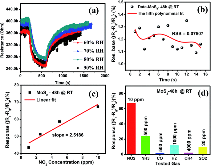 |
| | Fig. 8 (a) Transient resistance curves of the sensor based on the MoS2-48h sample to 1 ppm NO2 at RT under the different RHs. (b) Fifth polynomial fit of the baseline data of the response curve. (c) Linear fit of gas response versus NO2 gas concentrations. (d) Gas responses of the MoS2-48h sensor to interfering gases. | |
Although the sensor resistance varies with different RHs, the calculated gas response of the sensor relying on eqn (1) indicated an insignificant change with four measured RHs. This result demonstrated the RH-independent sensing characteristics of the MoS2 flower-based sensors at RT, which play an important role in developing a NO2 gas sensor working at RT for future integration into smart and/or portable devices.
In addition to the humidity effect, the DL and selectivity of the fabricated sensor are also important parameters for practical applications. Fig. 8(b) and (c) display the fifth-order polynomial fit of 15 experimental data points and the linear fit of the gas response as a function of NO2 concentrations at RT, respectively. On the basis of the fitting results, the DL value of the fabricated sensor was calculated as follows (12):51
| |
 | (12) |
where rms
noise is the root-mean-square standard deviation obtained from
Fig. 8(b), and Slope is extrapolated from the calibration curve obtained from
Fig. 8(c).
52,53 Namely, we took 15 experimental data points at the transient response baseline before exposing to NO
2 gas. The fifth-order polynomial fit of the 15 data points, as shown in
Fig. 8(b), provided the statistical parameters of the polynomial fit or residual sum of squares (RSS) of 0.07507, which was used to calculate the rms
noise:
| |
 | (13) |
where
Si and
S are the measured data point and corresponding value calculated from the fifth-order polynomial fitting equation;
N is the number of data points used for the fitting (
N = 15). Therefore, rms
noise was calculated to be 0.21223. The slope was extrapolated from the linear fitting in
Fig. 8(c), which was 2.5186 ppm. Thus, the DL was calculated using
eqn (12) to be 84 ppb, which allowed the RT sensor to detect the sub-ppm NO
2 concentration for practical applications.
Fig. 8(d) displays the gas response of the sensor based on the MoS2-48 h sample to different oxidising and reducing gases (10 ppm NO2, 20 ppm SO2, 500 ppm NH3, 500 ppm CO, 1000 ppm H2 and 4000 ppm CH4) at RT for the analysis of the selectivity properties of the sensor. The transient resistance curves of the sensor upon exposure to different gases are shown in Fig. S6(a)–(e) in ESI.† Although the concentration of the interfering gases was much higher than that of NO2 gas, the sensitivity of the sensor to NO2 gas was still much higher than to the interfering gases. This result can be explained by the stronger electronic interaction of NO2 gas with MoS2 owing to the higher adsorption energy of NO2 on the active sites of the MoS2 nanoflowers compared with the other tested gases.16,17 This result is consistent with previous theoretical calculations on the adsorption energy of various gases on MoS2 materials.54 The sensors based on the MoS2-48 h sample have good selectivity.
4. Conclusion
Sensors based on ultrathin MoS2 nanoflowers grown at different times of 24, 36, 48 and 60 h were fabricated by using the hydrothermal method. The morphology, crystal structure, composition and atomic structures of the grown MoS2 flower-like nanostructures were investigated using SEM, XRD, Raman spectroscopy, EDX and TEM. The results indicated the formation of well-defined crystal structure of the MoS2 nanoflowers comprising ultrathin petal-like nanosheets. The largest BET specific surface area of 56.57 m2 g−1 and smallest activation energy of 0.08 eV were obtained from the MoS2 nanoflowers grown for 48 h, which were responsible for enhancing the gas sensitivity of the sensor. The sensor based on the MoS2-48 h sample showed the highest gas sensitivity of 67.4% to 10 ppm NO2 at RT. The NO2 gas-sensing mechanism was discussed in detail. This sensor possessed a higher selectivity to NO2 gas compared with interfering gases (SO2, H2, CH4, CO and NH3), RH-independent sensing properties and a low detection limit of 84 ppb. The fabrication of RT gas sensors with RH-independent sensing property and good selectivity and detection limit opens up the future application of the sensor to smart, portable and IoT-based devices.
Conflicts of interest
There are no conflicts to declare.
Acknowledgements
This research was financially supported by the Ministry of Education and Training under Project No. B2018-BKA-08-CTrVL.
References
- N. Shehada, G. Brönstrup, K. Funka, S. Christiansen, M. Leja and H. Haick, Ultrasensitive silicon nanowire for real-world gas sensing: noninvasive diagnosis of cancer from breath volatolome, Nano Lett., 2015, 15, 1288–1295, DOI:10.1021/nl504482t.
- M. Donarelli and L. Ottaviano, 2D Materials for Gas Sensing Applications: A Review on Graphene Oxide, MoS2, WS2 and Phosphorene, Sensors, 2018, 18, 3638, DOI:10.3390/s18113638.
- A. J. Bandodkar, I. Jeerapan and J. Wang, Wearable Chemical Sensors: Present Challenges and Future Prospects, ACS Sens., 2016, 1, 464–482, DOI:10.1021/acssensors.6b00250.
- J. Park, J. Kim, K. Kim, S. Y. Kim, W. H. Cheong, K. Park, J. H. Song, G. Namgoong, J. J. Kim, J. Heo, F. Bien and J. U. Park, Wearable, wireless gas sensors using highly stretchable and transparent structures of nanowires and graphene, Nanoscale, 2016, 8, 10591–10597, 10.1039/c6nr01468b.
- T. H. Kim, Y. H. Kim, S. Y. Park, S. Y. Kim and H. W. Jang, Two-Dimensional Transition Metal Disulfides for Chemoresistive Gas Sensing: Perspective and Challenges, Chemosensors, 2017, 5, 15, DOI:10.3390/chemosensors5020015.
- M. W. Ahn, K. S. Park, J. H. Heo, J. G. Park, D. W. Kim, K. J. Choi, J. H. Lee and S. H. Hong, Gas sensing properties of defect-controlled ZnO-nanowire gas sensor, Appl. Phys. Lett., 2008, 93, 2006–2009, DOI:10.1063/1.3046726.
- P. L. Quang, N. D. Cuong, T. T. Hoa, H. T. Long, C. M. Hung, D. T. T. Le and N. Van Hieu, Simple post-synthesis of mesoporous p-type Co3O4 nanochains for enhanced H2S gas sensing performance, Sens. Actuators, B, 2018, 270, 158–166, DOI:10.1016/j.snb.2018.05.026.
- C. M. Hung, H. V. Phuong, N. Van Duy, N. D. Hoa and N. Van Hieu, Comparative effects of synthesis parameters on the NO2 gas-sensing performance of on-chip grown ZnO and Zn2SnO4 nanowire sensors, J. Alloys Compd., 2018, 765, 1237–1242, DOI:10.1016/j.jallcom.2018.06.184.
- M. Donarelli, S. Prezioso, F. Perrozzi, F. Bisti, M. Nardone, L. Giancaterini, C. Cantalini and L. Ottaviano, Response to NO2 and other gases of resistive chemically exfoliated MoS2-based gas sensors, Sens. Actuators, B, 2015, 207, 602–613, DOI:10.1016/j.snb.2014.10.099.
- C. Y. Wang, X. Zhang, Q. Rong, N. N. Hou and H. Q. Yu, Ammonia sensing by closely packed WO3 microspheres with oxygen vacancies, Chemosphere, 2018, 204, 202–209, DOI:10.1016/j.chemosphere.2018.04.050.
- S. Yang, C. Jiang and S. huai Wei, Gas sensing in 2D materials, Appl. Phys. Rev., 2017, 4, 021304, DOI:10.1063/1.4983310.
- D. J. Late, Y. K. Huang, B. Liu, J. Acharya, S. N. Shirodkar, J. Luo, A. Yan, D. Charles, U. V. Waghmare, V. P. Dravid and C. N. R. Rao, Sensing behavior of atomically thin-layered MoS2 transistors, ACS Nano, 2013, 7, 4879–4891, DOI:10.1021/nn400026u.
- F. K. Perkins, A. L. Friedman, E. Cobas, P. M. Campbell, G. G. Jernigan and B. T. Jonker, Chemical vapor sensing with monolayer MoS2, Nano Lett., 2013, 13, 668–673, DOI:10.1021/nl3043079.
- R. Lv, J. A. Robinson, R. E. Schaak, D. Sun, Y. Sun, T. E. Mallouk and M. Terrones, Transition metal dichalcogenides and beyond: synthesis, properties, and applications of single- and few-layer nanosheets, Acc. Chem.
Res., 2015, 48, 56–64, DOI:10.1021/ar5002846.
- H. Li, Z. Yin, Q. He, H. Li, X. Huang, G. Lu, D. W. H. Fam, A. I. Y. Tok, Q. Zhang and H. Zhang, Fabrication of single- and multilayer MoS 2 film-based field-effect transistors for sensing NO at room temperature, Small, 2012, 8, 63–67, DOI:10.1002/smll.201101016.
- R. Kumar, P. K. Kulriya, M. Mishra, F. Singh, G. Gupta and M. Kumar, Highly selective and reversible NO2 gas sensor using vertically aligned MoS2 flake networks, Nanotechnology, 2018, 29, 46400, DOI:10.1088/1361-6528/aade20.
- R. Kumar, N. Goel and M. Kumar, High performance NO2 sensor using MoS2 nanowires network, Appl. Phys. Lett., 2018, 112, 053502, DOI:10.1063/1.5019296.
- H. Miao, X. Hu, Q. Sun, Y. Hao, H. Wu, D. Zhang, J. Bai, E. Liu, J. Fan and X. Hou, Hydrothermal synthesis of MoS2 nanosheets films: microstructure and formation mechanism research, Mater. Lett., 2016, 166, 121–124, DOI:10.1016/j.matlet.2015.12.010.
- L. Yu, F. Guo, S. Liu, J. Qi, M. Yin, B. Yang, Z. Liu and X. H. Fan, Hierarchical 3D flower-like MoS2 spheres: post-thermal treatment in vacuum and their NO2 sensing properties, Mater. Lett., 2016, 183, 122–126, DOI:10.1016/j.matlet.2016.07.086.
- C. M. Lee, C. H. Jin, C. H. Ahn, H. K. Cho, J. H. Lim, S. M. Hwang and J. Joo, Enhanced Gas Sensing Performance of Surface-Activated MoS 2 Nanosheets Made by Hydrothermal Method with Excess Sulfur Precursor, Phys. Status Solidi A, 2019, 216, 1–6, DOI:10.1002/pssa.201800999.
- Y. Zhang, W. Zeng and Y. Li, Hydrothermal synthesis and controlled growth of hierarchical 3D flower-like MoS 2 nanospheres assisted with CTAB and their NO 2 gas sensing properties, Appl. Surf. Sci., 2018, 455, 276–282, DOI:10.1016/j.apsusc.2018.05.224.
- X. Xin, Y. Zhang, X. Guan, J. Cao, W. Li, X. Long and X. Tan, Enhanced Performances of PbS Quantum-Dots-Modified MoS 2 Composite for NO 2 Detection at Room Temperature, ACS Appl. Mater. Interfaces, 2019, 11, 9438–9447, DOI:10.1021/acsami.8b20984.
- L. T. Hong, V. A. Vuong, N. T. Thang and N. X. Thai, Effect of Hydrothermal Temperature on the Morphology and Structure of Synthesized MoS2 Nanostructures, J. Huazhong Univ. Sci. Technol., 2019, 138, 61–64 Search PubMed.
- N. D. Hoa, C. M. Hung, N. Van Duy and N. Van Hieu, Nanoporous and crystal evolution in nickel oxide nanosheets for enhanced gas-sensing performance, Sens. Actuators, B, 2018, 273, 784–793, DOI:10.1016/j.snb.2018.06.095.
- C. T. Quy, C. M. Hung, N. Van Duy, N. D. Hoa, M. Jiao and H. Nguyen, Ethanol-Sensing Characteristics of Nanostructured ZnO: Nanorods, Nanowires, and Porous Nanoparticles, J. Electron. Mater., 2017, 46, 3406–3411, DOI:10.1007/s11664-016-5270-2.
- N. Van Toan, C. M. Hung, N. Van Duy, N. D. Hoa, D. T. T. Le and N. Van Hieu, Bilayer SnO2–WO3 nanofilms for enhanced NH 3 gas sensing performance, Mater. Sci. Eng., B, 2017, 224, 163–170, DOI:10.1016/j.mseb.2017.08.004.
- G. Li, C. Li, H. Tang, K. Cao, J. Chen, F. Wang and Y. Jin, Synthesis and characterization of hollow MoS2 microspheres grown from MoO3 precursors, J. Alloys Compd., 2010, 501, 275–281, DOI:10.1016/j.jallcom.2010.04.088.
- Y. X. Zeng, X. W. Zhong, Z. Q. Liu, S. Chen and N. Li, Preparation and enhancement of
thermal conductivity of heat transfer oil-based MoS2 nanofluids, J. Nanomater., 2013, 2013, 1–6, DOI:10.1155/2013/270490.
- L. Sun, W. S. Leong, S. Yang, M. F. Chisholm, S.-J. Liang, L. K. Ang, Y. Tang, Y. Mao, J. Kong and H. Y. Yang, Concurrent Synthesis of High-Performance Monolayer Transition Metal Disulfides, Adv. Funct. Mater., 2017, 1605896, DOI:10.1002/adfm.201605896.
- H. Li, Q. Zhang, C. C. R. Yap, B. K. Tay, T. H. T. Edwin, A. Olivier and D. Baillargeat, From bulk to monolayer MoS2: Evolution of Raman scattering, Adv. Funct. Mater., 2012, 22, 1385–1390, DOI:10.1002/adfm.201102111.
- G. L. Frey and R. Tenne, Raman and resonance Raman investigation of MoS 2 nanoparticles, Phys. Rev. B, 2000, 60, 2883–2892, DOI:10.1103/PhysRevB.60.2883.
- L. Ye, H. Xu, D. Zhang and S. Chen, Synthesis of bilayer MoS2 nanosheets by a facile hydrothermal method and their methyl orange adsorption capacity, Mater. Res. Bull., 2014, 55, 221–228, DOI:10.1016/j.materresbull.2014.04.025.
- A. Gaber, M. A. Abdel-Rahim, A. Y. Abdel-Latief and M. N. Abdel-Salam, Influence of calcination temperature on the structure and porosity of nanocrystalline SnO2 synthesized by a conventional precipitation method, Int. J. Electrochem. Sci., 2014, 9, 81–95 Search PubMed.
- P. H. Phuoc, C. M. Hung, N. Van Toan, N. Van Duy, N. D. Hoa and N. Van Hieu, One-step fabrication of SnO2 porous nanofiber gas sensors for sub-ppm H2S detection, Sens. Actuators, A, 2019, 111722, DOI:10.1016/j.sna.2019.111722.
- P. Zhang, G. Pan, B. Zhang, J. Zhen and Y. Sun, High sensitivity ethanol gas sensor based on Sn-doped ZnO under visible light irradiation at low temperature, Mater. Res., 2014, 17, 817–822, DOI:10.1590/1516-1439.235713.
- Y. Han, D. Huang, Y. Ma, G. He, J. Hu, J. Zhang, N. Hu, Y. Su, Z. Zhou, Y. Zhang and Z. Yang, Design of Hetero-Nanostructures on MoS2 Nanosheets to Boost NO2 Roomerature Sensing, ACS Appl. Mater. Interfaces, 2018, 10, 22640–22649, DOI:10.1021/acsami.8b05811.
- H. Long, A. Harley-Trochimczyk, T. Pham, Z. Tang, T. Shi, A. Zettl, C. Carraro, M. A. Worsley and R. Maboudian, High Surface Area MoS2/Graphene Hybrid Aerogel for Ultrasensitive NO2 Detection, Adv. Funct. Mater., 2016, 26, 5158–5165, DOI:10.1002/adfm.201601562.
- C. M. Lee, G. C. Park, C. H. Ahn, J. W. Choi, C. H. Park, H. K. Cho, J. H. Lim and J. Joo, Effects of Precursor Concentration on Dimensional Size, Defect State, and Gas Sensing Performance of MoS2 Sheets Synthesized by Hydrothermal Method, Phys. Status Solidi A, 2018, 215, 1–5, DOI:10.1002/pssa.201800079.
- H. Li, Z. Yin, Q. He, H. Li, X. Huang, G. Lu, D. W. H. Fam, A. I. Y. Tok, Q. Zhang and H. Zhang, Fabrication of single- and multilayer MoS 2 film-based field-effect transistors for sensing NO at room temperature, Small, 2012, 8, 63–67, DOI:10.1002/smll.201101016.
- W. Li, Y. Zhang, X. Long, J. Cao, X. Xin, X. Guan, J. Peng and X. Zheng, Gas Sensors Based on Mechanically Exfoliated MoS2 Nanosheets for Room-Temperature NO2 Detection, Sensors, 2019, 19, 1–12, DOI:10.3390/s19092123.
- M. Ikram, L. Liu, Y. Liu, L. Ma, H. Lv, M. Ullah, L. He, H. Wu, R. Wang and K. Shi, Fabrication and characterization of a high-surface area MoS2@WS2 heterojunction for the ultra-sensitive NO2 detection at room temperature, J. Mater. Chem. A, 2019, 7, 14602–14612, 10.1039/c9ta03452h.
- L. Van Duy, N. H. Hanh, D. N. Son, P. T. Hung, C. M. Hung, N. Van Duy, N. D. Hoa, N. Van Hieu and F. Ke, Facile Hydrothermal Synthesis of Two-Dimensional Porous ZnO Nanosheets for Highly Sensitive Ethanol Sensor, J. Nanomater., 2019, 2019, 1–7, DOI:10.1155/2019/4867909.
- A. P. Lee and B. J. Reedy, Temperature modulation in semiconductor gas sensing, Sens. Actuators, B, 1999, 60, 35–42, DOI:10.1016/S0925-4005(99)00241-5.
- N. Barsan and U. Weimar, Conduction Model of Metal Oxide Gas Sensors, J. Electroceram., 2001, 7, 143–167, DOI:10.1023/A:1014405811371.
- A. Mortezaali and R. Moradi, The correlation between the substrate temperature and morphological ZnO nanostructures for H2S gas sensors, Sens. Actuators, A, 2014, 206, 30–34, DOI:10.1016/j.sna.2013.11.027.
- M. B. Rahmani, S. H. Keshmiri, M. Shafiei, K. Latham, W. Wlodarski, J. Du Plessis and K. Kalantar-Zadeh, Transition from n- to p-type of spray pyrolysis deposited Cu doped ZnO thin films for NO2 sensing, Sens. Lett., 2009, 7, 621–628, DOI:10.1166/sl.2009.1121.
- G. Deokar, P. Vancsó, R. Arenal, F. Ravaux, J. Casanova-Cháfer, E. Llobet, A. Makarova, D. Vyalikh, C. Struzzi, P. Lambin, M. Jouiad and J. F. Colomer, MoS2–Carbon Nanotube Hybrid Material Growth and Gas Sensing, Adv. Mater. Interfaces, 2017, 4, 1–10, DOI:10.1002/admi.201700801.
- Z. Bai, C. Xie, M. Hu, S. Zhang and D. Zeng, Effect of humidity on the gas sensing property of the tetrapod-shaped ZnO nanopowder sensor, Mater. Sci. Eng., B, 2008, 149, 12–17, DOI:10.1016/j.mseb.2007.11.020.
- P. Shankar and J. Rayappan, Gas sensing mechanism of metal oxides: the role of ambient atmosphere, type of semiconductor and gases-A review, Sci. Lett. J., 2015, 4, 126 Search PubMed.
- Y. Li, Z. Song, Y. Li, S. Chen, S. Li, Y. Li, H. Wang and Z. Wang, Hierarchical hollow MoS2 microspheres as materials for conductometric NO2 gas sensors, Sens. Actuators, B, 2019, 282, 259–267, DOI:10.1016/j.snb.2018.11.069.
- H. M. Tan, C. Manh Hung, M. N. Trinh, H. Nguyen, N. Duc Hoa, N. Van Duy and N. Van Hieu, Novel self-heated gas sensors using on-chip networked nanowires with ultralow power consumption, ACS Appl. Mater. Interfaces, 2017, 6b14516, DOI:10.1021/acsami.6b14516.
- G. Jeevitha, R. Abhinayaa, D. Mangalaraj, N. Ponpandian, P. Meena, V. Mounasamy and S. Madanagurusamy, Porous reduced graphene oxide (rGO)/WO 3 nanocomposites for the enhanced detection of NH 3 at room temperature, Nanoscale Adv., 2019, 1, 1799–1811, 10.1039/c9na00048h.
- N. Van Hoang, C. M. Hung, N. D. Hoa, N. Van Duy, I. Park and N. Van Hieu, Excellent detection of H2S gas at ppb concentrations using ZnFe2O4 nanofibers loaded with reduced graphene oxide, Sens. Actuators, B, 2019, 876–884, DOI:10.1016/j.snb.2018.11.157.
- S. Zhao, J. Xue and W. Kang, Gas adsorption on MoS2 monolayer from first-principles calculations, Chem. Phys. Lett., 2014, 595–596, 35–42, DOI:10.1016/j.cplett.2014.01.043.
- Y. Zhou, C. Zou, X. Lin and Y. Guo, UV light activated NO2 gas sensing based on Au nanoparticles decorated few-layer MoS2 thin film at room temperature, Appl. Phys. Lett., 2018, 113, 2–7, DOI:10.1063/1.5042061.
- S. Zhao, Z. Li, G. Wang, J. Liao, S. Lv and Z. Zhu, Highly enhanced response of MoS2/porous silicon nanowire heterojunctions to NO 2 at room temperature, RSC Adv., 2018, 8, 11070–11077, 10.1039/c7ra13484c.
- S. Y. Cho, S. J. Kim, Y. Lee, J. S. Kim, W. Bin Jung, H. W. Yoo, J. Kim and H. T. Jung, Highly Enhanced Gas Adsorption Properties in Vertically Aligned MoS2 Layers, ACS Nano, 2015, 9, 9314–9321, DOI:10.1021/acsnano.5b04504.
- J. Huang, J. Chu, Z. Wang, J. Zhang, A. Yang, X. Li, C. Gao, H. Huang, X. Wang, Y. Cheng and M. Rong, Chemisorption of NO2 to MoS2 Nanostructures and its Effects for MoS2 Sensors, ChemNanoMat, 2019, 5, 1123–1130, DOI:10.1002/cnma.201900350.
- Y. Kang, S. Pyo, E. Jo and J. Kim, Light-assisted recovery of reacted MoS2 for reversible NO2 sensing at room temperature, Nanotechnology, 2019, 30, 355504, DOI:10.1088/1361-6528/ab2277.
Footnote |
| † Electronic supplementary information (ESI) available. See DOI: 10.1039/d0ra00121j |
|
| This journal is © The Royal Society of Chemistry 2020 |
Click here to see how this site uses Cookies. View our privacy policy here. 
 Open Access Article
 This Open Access Article is licensed under a Creative Commons Attribution-Non Commercial 3.0 Unported Licence
 *a,
Nguyen Van Duy*a,
Nguyen Van Hieu
*a,
Nguyen Van Duy*a,
Nguyen Van Hieu


 ; or
; or 


