
 Open Access Article
 This Open Access Article is licensed under a Creative Commons Attribution-Non Commercial 3.0 Unported Licence
Designing coexisting multi-phases in PZT multilayer thin films: an effective way to induce large electrocaloric effect
Cai Chena,
Sichun Wangac,
Tiandong Zhang *ab,
Changhai Zhangab,
Qingguo Chi*ab and
Weili Li*d
*ab,
Changhai Zhangab,
Qingguo Chi*ab and
Weili Li*d
aSchool of Electrical and Electronic Engineering, Harbin University of Science and Technology, Harbin 150080, PR China. E-mail: tdzhang@hrbust.edu.cn
bKey Laboratory of Engineering Dielectrics and Its Application, Ministry of Education, Harbin University of Science and Technology, Harbin 150080, PR China
cSchool of Electrical Engineering and Automation, Harbin Institute of Technology, Harbin 150001, PR China
dSchool of Materials Science and Engineering, Harbin Institute of Technology, Harbin 150001, PR China
First published on 12th February 2020
Abstract
Coexisting multi-phases in PbZrxTi1−xO3 multilayer thin films were successfully fabricated using the sol–gel method. The microstructure and electrical of the multilayer films with different growth sequences, including the up multilayer films and down multilayer films, have been systematically investigated. The results indicate that a large electrocaloric effect (ECE) is obtained at the temperatures much below the Curie temperature. At room temperature (25 °C), the change in temperature (ΔT) values of the up multilayer and down multilayer thin films are 20.2 K with the applied electric field E = 826 kV cm−1 and 46.3 K with the E = 992 kV cm−1, respectively. In addition, both the films exhibit outstanding ECE of around 145 °C, and ΔT values of 28.9 K and 14.8 K have been obtained for the up multilayer and down multilayer thin films. The results indicate that the antiferroelectric/ferroelectric (AFE/FE), ferroelectric/ferroelectric (FE/FE) phase transition and the synergistic effect of the AFE/FE and FE/FE phase transition are as effective as the FE/PE phase transition. In particular, the multilayer thin films are endowed with refrigeration ability at multi-temperature zones due to the coexistence of multi-phases.
Introduction
Caloric materials, including electrocaloric, magnetocaloric, piezocaloric and elastocaloric materials, have attracted considerable attention in recent years due to their applications in various technological fields.1–5 Electrocaloric effect (ECE) is considered to be one of the most important thermodynamic effects employed in refrigeration technologies.6,7 Electrocaloric materials, such as inorganic ferroelectrics,8–10 relaxor ferroelectrics,11,12 and organic polymer films,13,14 have been widely studied. The electrocaloric effect is a change in the temperature (ΔT) of a ferroelectric (FE) material by the change in entropy (ΔS) upon the application or withdrawal of an electric field under adiabatic conditions. The maximum ΔT values are mostly obtained near the point of first order phase transition and confined to Curie temperature (Tc), which is much higher than the room temperature. For example, Mischenko et al. reported that ΔT = 12 K and ΔS = 8 J K−1 kg−1 at 222 °C for PbZr0.95Ti0.05O3 thin films were obtained due to ferroelectric/paraelectric (FE/PE) phase transition.6 For the Pb0.97La0.02(Zr0.65Sn0.3Ti0.05)O3 thin film, ΔT = 20.1 K was obtained at a temperature corresponding to the antiferroelectric (AFE) phase to paraelectric phase transition.15 Although a high working temperature may permit cooling applications in many fields, such as automotive, aerospace, or food industries, a lower working temperature is also important and can be used in on-chip refrigeration or other fields. In particular, lower working temperatures are also beneficial to reduce the films fatigue, entitling them with higher breakdown strength.In the consideration of viewpoints mentioned above, exploring an effective way to reduce the working temperature of electrocaloric materials is very significant for the further expansion of their applications. It was reported that with regards to the ECE of the doped PbZrxTi1−xO3 (PZT) thin films, including PNZST16 and PLZST,17 which originated from the phase transition between AFE and FE, the ΔT values are 5.5 K and 3.8 K near the room temperature, respectively. A large ΔT (45.3 K) in Pb0.8Ba0.2ZrO3 AFE thin films was observed at room temperature due to the coexistence of the AFE and FE phases at the nanoscale.18 Besides, the 0.7Pb(Mg1/3Nb2/3)O3-0.3PbTiO3 and PbZr0.52Ti0.48O3 thin films were prepared and at morphotropic phase boundary (MPB), the compositions were investigated, which demonstrated that low temperature refrigeration can be realized by utilizing the phase transition at MPB.19 Hence, it can be concluded that not only the phase transition between FE/PE phases, but also one of the AFE/FE phases or FE/FE phases act as the potential sources for excellent ECE. Furthermore, a theoretical analysis for developing ferroelectric materials with high ECE near an invariant critical point (ICP) was proposed; the enhanced ECE can be attributed to the increase in the entropy induced by the coexisting multi-phases.20
In order to build coexisting multi-phases in electrocaloric materials, in this study, the PbZrxTi1−xO3 multilayer thin films were fabricated on a Pt(111)/Ti/SiO2/Si substrate. As shown in Fig. 1(a) and (b), the PbZr0.95Ti0.05O3, PbZr0.8Ti0.2O3 and PbZr0.52Ti0.48O3 individual layers can provide an antiferroelectric orthorhombic phase, rhombohedral phase and morphotropic phase, respectively.21 The results indicate that the ECE can be enhanced by making use of the phase transition in the individual layer, and the synergistic effect of AFE/FE and FE/FE phase transitions is as effective as the effect of FE/PE phase transition. In particular, the multilayer thin films are endowed with refrigeration ability at the multi-temperature zones due to the coexisting multi-phases. The results further confirmed that the construction of bilayer or five-layer films is an effective way to enhance the ECE of PZT-based films, similar to our previous studies.22,23 In order to further confirm the validity of enhancing ECE by constructing coexisting multi-phases, in this study, the ECE effect of three-layered PZT films have been systematically investigated.
 | ||
| Fig. 1 Schematics of PbZrxTi1−xO3 multilayer thin films: (a) up multilayer thin films; (b) down multilayer thin films. (c) XRD patterns of the multilayer thin films. | ||
Experimental section
Fabrication of multilayer films
First, the precursor solution was prepared. Pb(CH3COO)2·3H2O (Sinopharm Chemical Reagent Co. Ltd, ≧99.5%) was dissolved in 2-methoxyethanol (Sinopharm Chemical Reagent Co. Ltd, ≧99%) and refluxed at 120 °C for half an hour. After the solution was cooled down to room temperature, titanium isopropoxide (Alfa, 99%) and zirconium n-propoxide (Alfa, 70% w/w in n-propanol) were added, in sequence. After refluxing for an hour, the concentration of the solution was adjusted to 0.4 mol L−1 by adjusting the volume of 2-methoxyethanol. Moreover, 10 mol% excess of Pb(CH3COO)2·3H2O was used to compensate the lead volatility during the processing. After aging the precursor solution for 24 hours, PbZrxTi1−xO3 multilayer thin films were deposited on Pt(111)/Ti/SiO2/Si substrates through a spin coating process at 4000 rpm for 15 s. The deposition of each layer was followed by pyrolysis at 375 °C for 3 min, and each composition was spin coated for two layers. The total thickness of the films was determined by regulating the number of spin coatings. At last, the multilayer thin films were annealed via rapid temperature annealing (RTA) at 700 °C for 5 min.Microstructure characteristics
The crystalline structures of the thin films were analyzed using a Philips X′ pert X-ray diffractometer (XRD) with Cu Kα radiation generated at 40 kV and 40 mA. The surface morphology of the thin films was observed by atomic force microscopy (AFM) using a commercial setup of a scanning probe microscope system (CSPM5600 of Benyuan), and the cross-section micrograph of the thin film was obtained by SEM (Helios Nanolab600i) with an accelerating voltage of 20 kV.Electrical measurements
Platinum top electrodes with a diameter of 200 μm were deposited by DC magnetron sputtering. Ferroelectric properties were measured using a Radiant Precision Workstation Ferroelectric Measurement System; three unique electrodes were tested for each sample. With the help of the Agilent 4294A precision impedance analyzer, the temperature dependence of the dielectric properties of the samples was measured at the frequency of 10 kHz with a 500 mV AC amplitude. The capacitance of the samples with the applied electric field was measured at 1 MHz with a 50 mV ac amplitude. The temperature was increased from room temperature (25 °C) to 180 °C using a Sigma heating system with the heating rate of 3 °C min−1.Results and discussion
Microstructure
The XRD diffraction patterns shown in Fig. 1 indicate that both the up multilayer films and down multilayer films have a pure perovskite structure without any trace of secondary phases. The multi-phases, namely the orthorhombic AFE (OAFE) phase originating from the PbZr0.95Ti0.05O3 layer, the rhombohedral FE (RFE) phase originating from the PbZr0.8Ti0.2O3 layer and the tetragonal FE (TFE) phase originating from the PbZr0.52Ti0.48O3 layer, are observed and coexist in the multilayer films. Since the PbZrxTi1−xO3 layer, which is closer to the Pt(111)/Ti/SiO2/Si substrate, possesses a different crystal lattice constant, the mismatch stress between the bottom PbZrxTi1−xO3 layer and Pt layer leads to the mixed orientation of (100) and (111) in the up multilayer films and (110) orientation in the down multilayer films; these results are in accordance with those obtained in our previous study.22AFM and SEM were carried out to characterize the surface morphology and cross-sectional morphology of the multilayer thin films, as shown in Fig. 2. The up multilayer films exhibited fine grains (size = ∼90 nm) and dense surface structure. The down multilayer thin films, showed larger grain size (size = ∼2 μm) and clear grain boundaries, while some fine grains (size = ∼100 nm) can be seen on the surface of larger grains. The surface morphologies observed via SEM, as shown in Fig. 2(c) and (d), are consistent with that of the AFM images. It was reported that the activation energy for nucleation decreased with the increase in the Ti content in the PZT films.24,25
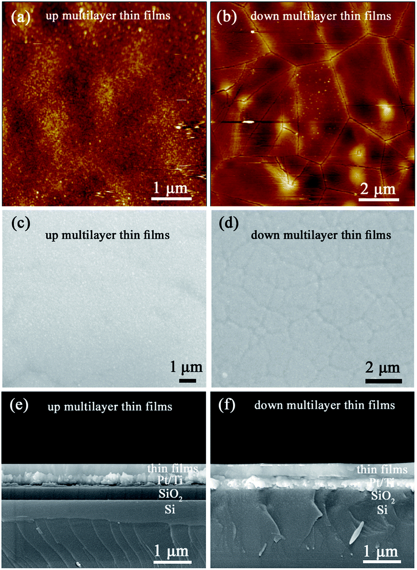 | ||
| Fig. 2 AFM images of (a) up multilayer thin films and (b) down multilayer thin films. SEM images of the surface of (c) up multilayer thin films and (d) down multilayer thin films. SEM cross-sectional images of (e) up multilayer thin films and (f) down multilayer thin films. | ||
In this study, the PbZr0.95Ti0.05O3 layer acts as the top layer for the up multilayer films, where the Zr-rich layer leads to the smaller grain size. For the down multilayer films, the Ti-rich layer of PbZr0.52Ti0.48O3 possesses lower nucleation energy and results in the larger grain size.24,25 The cross-sectional images of the multilayer films are given in Fig. 2(e) and (f); the results indicate that the thickness of the multilayer films is approximately 300 nm. The differences in the microstructure of the up and down multilayer films are mainly induced by the different growth sequences. It was also reported that the grain size, thickness effects, substrates and associated processing conditions had deep influences on the electrical responses of PZT-based films.26–28
Dielectric properties
The dielectric spectra, namely those of the temperature dependence of the dielectric properties and the characteristics of capacitance with applied electric field, are always used to investigate the phase structure and the phase transition behaviour of the materials. In this study, the dielectric constant (εr) and loss were measured using an Agilent 42941A impedance analyzer at 10 kHz and 500 mV ac amplitude; the temperature was increased from room temperature (25 °C) to 180 °C by the Sigma heating system with the heating rate of 3 °C min−1. The capacitance of the samples with the applied electric field was measured at 1 MHz.In Fig. 3, it can be seen that the spectrum of the up multilayer thin films shows an unclear peak at 120 °C, which is associated with the OAFE/RFE phase transition of the PbZr0.95Ti0.05O3 layer, according to the PZT phase diagram.21 It needs to be stressed that no peak corresponding to the AFE/FE transition was observed in the curve of the PbZr0.95Ti0.05O3 single layer thin film.6 The dielectric constant of the down multilayer thin films has a broad peak corresponding to the R(FE, LT)/R(FE, HT) phase transition of the PbZr0.8Ti0.2O3 layer at around 150 °C.21 The broadening of the peak is typical in the curves of thin films, and may be induced by the interfacial strain and concentration gradients. In addition, the temperature dependence of the dielectric constant and dielectric loss around the room temperature indicates the phase transition of RFE/TFE in the PbZr0.52Ti0.48O3 MPB composite, but the OAFE/RFE phase transition in the PbZr0.95Ti0.05O3 antiferroelectric layer cannot be observed at room temperature. The up and down multilayer films exhibit different variation trends of the dielectric spectrum, which implies that the thin film growth sequence has a deep influence on the phase transition of AFE/FE and FE/FE, which may be caused by the different misfit strain in the multilayer thin films.
 | ||
| Fig. 3 Temperature dependence of the dielectric properties measured at 10 kHz for (a) up multilayer films and (b) down multilayer films. The capacitance with the applied electric field measured at 1 MHz for (c) up multilayer films and (d) down multilayer thin films. | ||
The applied electric field dependence of capacitance of the up and down multilayer films is shown in Fig. 3(c) and (d), respectively. It was reported that the capacitance vs. applied electric field of the AFE or FE thin films displays a double butterfly shape23 and a single butterfly shape, respectively.29 When a lower electric field of 175 kV cm−1 is applied, as shown in the insets of Fig. 3, the non-asymmetric curves of capacitance with the applied electric field can be observed, which demonstrates the coexistence of AFE phase and FE phase in the multilayer films. In particular, the AFE characteristic in the down multilayer thin films were more distinct than that in the up multilayer thin films. When the applied electric field reaches 500 kV cm−1, the curves exhibit single butterfly characteristics, which indicates that only the FE phase existed in the multilayer films due to the electric field-induced AFE/FE phase transition.
Electrocaloric effect
An in-direct method was employed to evaluate the ECE of the multilayer thin films. The dependence of hysteresis loops (abbreviated as P(E)) on temperature was measured at a frequency of 100 Hz at a 5 K interval from 25 °C to 160 °C. A lower electric field of 826 kV cm−1 was applied for the up multilayer thin films and a higher electric field of 992 kV cm−1 was applied for the down multilayer thin films. The representative hysteresis loops given in Fig. 4(a) and (b) correspond to the up multilayer and down multilayer thin films. The shape of P(E) loops exhibits some differences between the up and down multilayer films, which may be caused by the microstructure differences, such as mismatch stress and grain size, induced by the different growth sequence.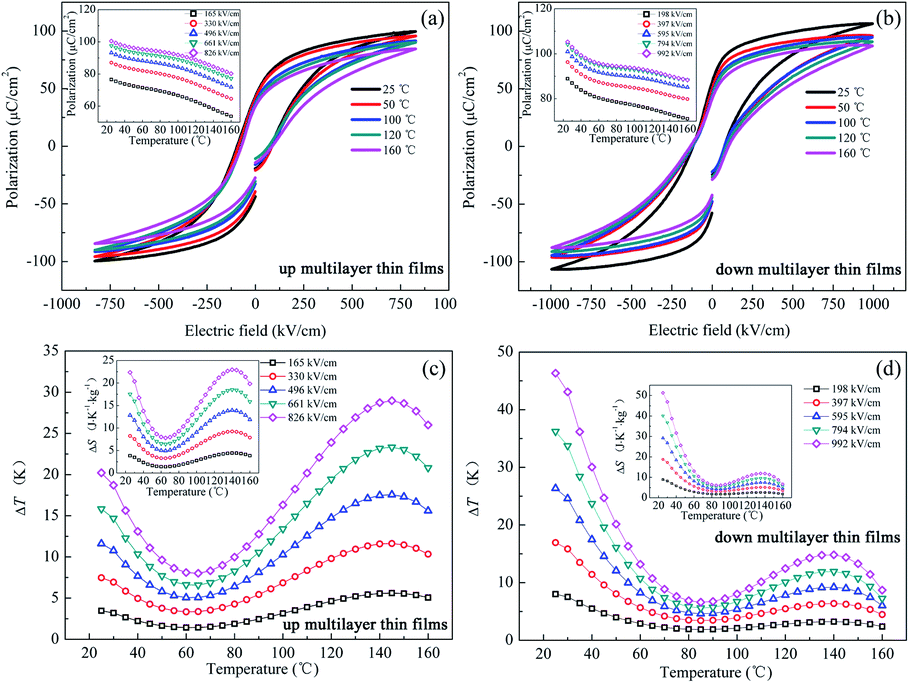 | ||
| Fig. 4 P(E) loops at selected temperatures for (a) up multilayer thin films and (b) down multilayer thin films. ΔT at selected electric fields for (c) up multilayer thin films and (d) down multilayer thin films. | ||
We assumed the reversible adiabatic changes following the Maxwell relationship, as shown in eqn (1), and the temperature change ΔT and entropy change ΔS for a material of density ρ with specific heat capacity C are expressed in eqn (2) and (3):6,7
 | (1) |
 | (2) |
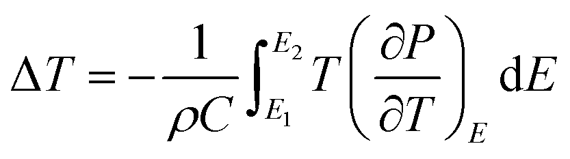 | (3) |
The values of (∂P/∂T) were obtained from the fourth-order polynomial fits to the P(T) data extracted from the upper branches of P(E) loops in E > 0 (see the inset of Fig. 4(a) and (b)). According to the composition of each layer in the multilayer films, both the up multilayer and down multilayer thin films can be considered as Zr-rich lead-based thin films. The heat capacity C = 330 J K−1 kg−1 and density ρ = 8.3 kg cm−3 can be selected for the Zr-rich lead-based thin films.6,17 As shown in Fig. 4(c) and (d), as expected, ΔT = 20.2 K for the up multilayer thin films and ΔT = 46.3 K for the down multilayer thin films are achieved at room temperature, which are mainly induced by the phase transition of RFE/TFE at MPB in the PbZr0.52Ti0.48O3 layer and OAFE/RFE in the PbZr0.95Ti0.05O3 layer. It was reported that the presence of the monoclinic (MA, MB) phases between the RFE and TFE phase transition makes the lattice more frustrated and causes huge ΔS and ΔT values,19 particularly accompanying AFE/FE phase transition under electric field.18 It is also worth mentioning that both the films exhibit outstanding ECE at around 145 °C, much below the Tc. The peak of ΔT = 28.9 K and 14.8 K for the up multilayer thin films and down multilayer thin films is observed, which is mainly attributed to the AFE/FE phase transition of the PbZr0.95Ti0.05O3 layer and the FE/FE phase transition of the PbZr0.8Ti0.2O3 layer and PbZr0.52Ti0.48O3 layer according to the relationship between the dielectric constant and temperature. Insets of Fig. 4(c) and (d) give the entropy change ΔS with the increase in temperature. The maximum ΔS is 22.8 J K−1 kg−1 and 51.2 J K−1 kg−1 for the up and down multilayer thin films, respectively. The ECE improved significantly in comparison with our previous study, which may be attributed to the negative effect of the PbZrO3 antiferroelectric layer.22 Honestly, besides the synergistic effect of multi-phases transition, which is one of the key factors to enhance the ECE, the effect of the domain architecture,30 polarization,31 electrostatic interactions32 and misfit strain33 in the multilayer films should be deeply investigated in further studies, as they may also play an important role in the enhancement of ECE in the multilayer thin films compared with the single-layer thin films. For comparison, Table 1 lists the electrocaloric effect of the representative lead-containing materials, where it can be found that the PZT multilayer films possess excellent ECE both at room temperature and around 145 °C.
| Materials | ΔT (K) | ΔS (J K−1 kg−1) | Phase transition | T (°C) | Ref. |
|---|---|---|---|---|---|
| PZT up multilayer films | 20.2 | 22.3 | AFE/FE | 25 | This work |
| 28.9 | 22.8 | FE/FE | 145 | ||
| PZT down multilayer films | 46.3 | 51.2 | AFE/FE | 25 | This work |
| 14.8 | 11.8 | FE/FE | 140 | ||
| PbZr0.95Ti0.05O3 | 12 | 8 | AFE/PE | 226 | 6 |
| Si doped PbZr0.95Ti0.05O3 | 8.5 | 5.89 | AFE/PE | 203 | 37 |
| PbZrO3 | 11.4 | — | AFE/PE | 235 | 34 |
| Pb0.97La0.02Zr0.75Sn0.18Ti0.07O3 | 53.8 | 63.9 | AFE/FE | 5 | 16 |
| Pb0.8Ba0.2ZrO3 | 45.3 | 46.9 | AFE/FE | 17 | 18 |
| PbZr0.52Ti0.48O3 | 11.1 | — | FE/FE | 387 | 19 |
| PMN-PT 67/33 | 14.5 | — | FE/PE | 150 | 35 |
| PbZr0.95Ti0.05O3/PbZr0.52Ti0.48O3 bilayer films | 24.8 | 20.5 | AFE/FE | 125 | 23 |
| 10.7 | 11.9 | FE/FE | 25 | ||
| PZT multilayer films | 9.1 | 10 | AFE/FE | 25 | 22 |
| 17.9 | 13.1 | FE/FE | 180 | ||
| PZT/BaTiO3 multilayer films | 1.85 | — | FE/PE | 135 | 38 |
| PbZr0.53Ti0.47O3/CoFe2O4 multilayer films | −52.2 | 94.23 | — | −223 | 36 |
Leakage current I(t) measurements with their maximum field were investigated at 160 °C, as shown in Fig. 5. It can be seen that the steady-state leakage current for the up multilayer thin films and down multilayer thin films are 6 nA and 1.1 nA, respectively. The lower leakage current also indicates that the higher electric field can be applied for the down multilayer thin films. In addition, the less joule heat would be induced by the lower leakage current, which is beneficial for the refrigeration to work steadily.
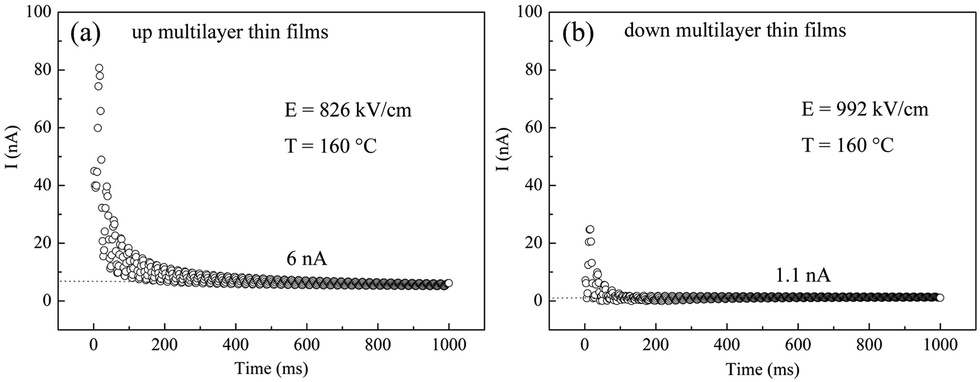 | ||
| Fig. 5 Leakage current measurements of multilayer films at 160 °C (a) up multilayer thin films and (b) down multilayer thin films. | ||
Conclusions
In summary, we experimentally showed that the ECE in PbZrxTi1−xO3 multilayer thin films can be significantly enhanced by the coupling effect of the AFE/FE phase transition and FE/FE phase transition. Our study highlights the importance of the multi-phases coexisting in the PbZrxTi1−xO3 multilayer thin films. The results presented for the up multilayer and down multilayer thin films demonstrate the potential to achieve a large ECE. ΔT = 20.2 K for the up multilayer thin films and ΔT = 46.3 K for the down multilayer thin films have been achieved at room temperature, and ΔT = 28.9 K and 14.8 K have also been observed in the up multilayer and down multilayer thin films, respectively. These results indicate that the AFE/FE or FE/FE phase transitions are as effective as the FE/PE phase transition, and large electrocaloric responses can be obtained at temperatures much below the Curie temperature.Conflicts of interest
There are no conflicts to declare.Acknowledgements
The authors gratefully acknowledge the support from the Natural Science Foundation of China (Grant No. 51807042, 51702069). China Postdoctoral Science Foundation (No. 2018M640303). Fundamental Research Foundation for Universities of Helongjiang Province (No. LGYC2018JC020). Cai Chen and Sichun Wang are co-first authors, and contributed equally to this study.Notes and references
- X. Moya, S. Kar-Narayan and N. D. Mathur, Nat. Mater., 2014, 13, 439–450 CrossRef PubMed.
- A. M. Tishin, Y. I. Spichkin, V. I. Zverev and P. W. Egolf, Int. J. Refrig., 2016, 68, 177–186 CrossRef.
- S. Lisenkov, R. Herchig, S. Patel, R. Vaish, J. Cuozzo and I. Ponomareva, Nano Lett., 2016, 16, 7008–7012 CrossRef PubMed.
- S. Lisenkov, B. K. Mani, J. Cuozzo and I. Ponomareva, Phys. Rev. B, 2016, 93, 064108 CrossRef.
- X. Moya, E. Defay, V. Heine and N. D. Mathur, Nat. Phys., 2015, 11, 202–205 Search PubMed.
- A. S. Mischenko, Q. Zhang, J. F. Scott, R. W. Whatmore and N. D. Mathur, Science, 2006, 311, 1270 CrossRef PubMed.
- B. Neese, B. J. Chu, S. G. Lu, Y. Wang, E. Furman and Q. M. Zhang, Science, 2008, 321, 821–823 CrossRef PubMed.
- J. Tušek, K. Engelbrecht, R. Millán-Solsona, L. Mañosa, E. Vives, L. P. Mikkelsen and N. Pryds, Adv. Energy Mater., 2015, 5, 1500361 CrossRef.
- M. H. Park, H. J. Kim, Y. J. Kim, T. Moon, K. D. Kim and C. S. Hwang, Nano Energy, 2015, 12, 131–140 CrossRef.
- T. D. Zhang, W. L. Li, Y. F. Hou, Y. Yu, W. P. Cao, Y. Feng and W. D. Fei, RSC Adv., 2016, 6, 71934 RSC.
- A. Gupta, R. Kumar and S. Singh, Scr. Mater., 2018, 143, 5–9 CrossRef.
- Z. J. Jiang, S. Prokhorenko, S. Prosandeev, Y. Nahas, D. Wang, J. Íñiguez, E. Defay and L. Bellaiche, Phys. Rev. B, 2017, 96, 014114 CrossRef.
- R. J. Ma, Z. Y. Zhang, K. Tong, D. Huber, R. Kornbluh, Y. Sungtaek and Q. B. Pei, Science, 2017, 357, 1130–1134 CrossRef PubMed.
- G. Z. Zhang, L. X. Weng, Z. Y. Hu, Y. Liu, R. X. Bao, P. Zhao, H. Feng, N. Yang, M.-Y. Li, S. L. Zhang, S. L. Jiang and Q. Wang, J. Alloys Compd., 2018, 731, 489–495 CrossRef.
- B. L. Peng, Q. Zhang, Y. N. Lyu, L. J. Liu, X. J. Lou, C. Shaw, H. T. Huang and Z. L. Wang, Nano Energy, 2018, 47, 285–293 CrossRef.
- X. H. Hao and J. W. Zhai, Appl. Phys. Lett., 2014, 104, 022902 CrossRef.
- Y. Zhao, X. H. Hao and Q. Zhang, J. Mater. Chem. C, 2015, 3, 1696–1697 RSC.
- B. L. Peng, H. Q. Fan and Q. Zhang, Adv. Funct. Mater., 2013, 23, 2987–2992 CrossRef.
- R. Chukka, J. W. Cheah, Z. H. Chen, P. Yang, S. Shannigrahi, J. L. Wang and L. Chen, Appl. Phys. Lett., 2011, 98, 242902 CrossRef.
- Z. K. Liu, X. Y. Li and Q. M. Zhang, Appl. Phys. Lett., 2012, 101, 082904 CrossRef.
- N. Zhang, H. Yokota, A. M. Glazer, Z. Ren, D. A. Keen, D. S. Keeble, P. A. Thomas and Z.-G. Ye, Nat. Commun., 2014, 5, 5231 CrossRef PubMed.
- T. D. Zhang, W. L. Li, Y. Yu, M. Wang, J. He and W. D. Fei, J. Alloys Compd., 2018, 731, 489–495 CrossRef.
- T. D. Zhang, W. L. Li, W. P. Cao, Y. F. Hou, Y. Yu and W. D. Fei, Appl. Phys. Lett., 2016, 108, 162902 CrossRef.
- F. C. Kartawidjaja, C. H. Sim and J. Wang, J. Mater. Sci., 2009, 44, 5375–5382 CrossRef.
- F. C. Kartawidjaja, A. Varatharajan, N. Valanoor and J. Wang, J. Mater. Sci., 2010, 45, 6187–6199 CrossRef.
- J. F. Ihlefeld, D. T. Harris, K. Ryan, L. Jacob, J.-P. M. Jones and S. Trolier-McKinstry, J. Am. Ceram. Soc., 2016, 99, 2537–2557 CrossRef.
- C. T. Shelton, P. G. Kotula, G. L. Brennecka, P. G. Lam, E. Kelsey, J.-P. M. Meyer, B. J. Gibbons and J. F. Ihlefeld, J. Am. Ceram. Soc., 2010, 93, 3935–3954 CrossRef.
- C. T. Shelton, P. G. Kotula, G. L. Brennecka, P. G. Lam, K. E. Meyer, J.-P. l. Maria, B. J. Gibbons and J. F. Ihlefeld, Adv. Funct. Mater., 2012, 22, 2295–2302 CrossRef.
- M. Ye, H. T. Huang, T. Li, S. M. Ke, P. Lin, B. L. Peng, M. F. Mai, Q. Sun, X. Peng and X. R. Zeng, Appl. Phys. Lett., 2015, 107, 202902 CrossRef.
- R. V. K. Mangalam, J. Karthik, A. R. Damodaran, J. C. Agar and L. W. Martin, Adv. Mater., 2013, 25, 1761–1767 CrossRef.
- Z. Kutnjak and R. Blinc, Phys. Rev. B, 2007, 76, 104102 CrossRef.
- M. T. Kesim, J. Zhang, S. P. Alpay and L. W. Martin, Appl. Phys. Lett., 2014, 105, 052901 CrossRef.
- J. H. Qiu and Q. Jiang, J. Appl. Phys., 2008, 103, 084105 CrossRef.
- J. Parui and S. B. Krupanidhi, Phys. Status Solidi A, 2008, 5, 230–232 Search PubMed.
- Z. Y. Feng, D. Q. Shi and S. X. Dou, Solid State Commun., 2011, 151, 123–126 CrossRef.
- G. Vats, A. Kumar, N. Ortega, C. R. Bowen and R. S. Katiyar, Energy Environ. Sci., 2016, 9, 1335–1345 RSC.
- J. X. Wang, G. C. Jiang, W. C. Huang, D. Q. Liu, B. Yang and W. W. Cao, Appl. Phys. Lett., 2019, 115, 053901 CrossRef.
- M.-S. Kwon, S.-G. Lee and K.-M. Kim, J. Nanosci. Nanotechnol., 2018, 18, 5936–5941 CrossRef CAS.
| This journal is © The Royal Society of Chemistry 2020 |