DOI:
10.1039/C9RA10771A
(Paper)
RSC Adv., 2020,
10, 7839-7854
Enhancement in the performance of nanostructured CuO–ZnO solar cells by band alignment†
Received
21st December 2019
, Accepted 14th February 2020
First published on 24th February 2020
Abstract
In this study, we investigated the effect of cobalt doping on band alignment and the performance of nanostructured ZnO/CuO heterojunction solar cells. ZnO nanorods and CuO nanostructures were fabricated by a low-temperature and cost-effective chemical bath deposition technique. The band offsets between Zn1−xCoxO (x = 0, 0.05, 0.10, 0.15, and 0.20) and CuO nanostructures were estimated using X-ray photoelectron spectroscopy and it was observed that the reduction of the conduction band offset with CuO. This also results in an enhancement in the open-circuit voltage. It was demonstrated that an optimal amount of cobalt doping could effectively passivate the ZnO related defects, resulting in a suitable conduction band offset, suppressing interface recombination, and enhancing conductivity and mobility. The capacitance–voltage analysis demonstrated the effectiveness of cobalt doping on enhancing the depletion width and built-in potential. Through impedance spectroscopy analysis, it was shown that recombination resistance increased up to 10% cobalt doping, thus decreased charge recombination at the interface. Further, it was demonstrated that the insertion of a thin layer of molybdenum oxide (MoO3) between the active layer (CuO) and the gold electrode hinders the formation of a Schottky junction and improved charge extraction at the interface. The ZnO/CuO solar cells with 10% cobalt doped ZnO and 20 nm thick MoO3 buffer layer achieved the best power conversion efficiency of 2.11%. Our results demonstrate the crucial role of the band alignment on the performance of the ZnO/CuO heterojunction solar cells and could pave the way for further progress on improving conversion efficiency in oxide-based heterojunction solar cells.
1. Introduction
Fabrication of photovoltaic (PV) devices is critically dependent on the availability of low-cost materials used in the fabrication.1 For third-generation solar technologies, nanostructured materials are integrated into scalable, robust, and low-cost device structures that electronically couple the photoactive nanostructures to an external circuit. Metal oxides are abundant in nature and can be synthesized by inexpensive wet chemical methods with tunable electrical properties. With its excellent minority carrier diffusion length, high absorption coefficient, non-toxicity, and environmental friendly deposition methods, CuO has always been considered as a potential absorber material for low-cost photovoltaic applications.1,2 For a single p–n junction solar cell, the optimum bandgap is about 1.34 eV for maximum efficiency, the optical properties of CuO (bandgap 1.4 eV) serve as an excellent candidate for a semiconductor absorber material for solar cell application.3 Based on a Shockley–Queisser analysis of CuO-based solar cells, it is predicted to have a theoretical power conversion efficiency of around 30% by considering only radiative recombination.4 As there is no n-type CuO available, solar cells must be constructed as heterojunctions with another material as an n-type, wide bandgap window material.5 One n-type material that can be used for oxide-based solar cells is zinc oxide (ZnO) due to its wide bandgap and a relatively high absorption coefficient.3,5 Similarly, homo-junctions are challenging to form for ZnO because the p-type conductivity is very sensitive to the synthesis and post-treatment conditions.5,6 However, there are few reports of p-type ZnO available in the literature.7,8 Therefore, one of the best solutions for fabricating oxide-based solar cells will be to study a ZnO/CuO heterojunction as a stable p–n junction.3,9,10
Previously, few efforts have been focused on fabricating p-CuO/n-ZnO heterojunctions11–13 even though simple estimates predict large valence band offsets (VBOs) and conduction band offsets (CBOs) between the two semiconductors.14 Therefore, it is imperative to control the band alignments in CuO/ZnO for further enhancement of power conversion efficiency by altering conduction and valence band offsets. A heterojunction device based on ZnO nanowires coated with CuO nanoparticles has been reported with a power conversion efficiency of up to 0.3%.15 Omayio et al.16 reported a maximum efficiency of 0.23% for Sn-doped ZnO/CuO solar cells. In another literature,17 the maximum reported efficiency for CuO/ZnO nanocomposites-based device is 1.1 × 10⁻⁴%. By using the pulsed laser deposition (PLD) method, Bhaumik et al.18 reported the highest power conversion efficiency of 2.88% device of CuO nanostructure decorated with nanoparticles. For heterojunction solar cell, both the n-type and active absorber layer interface play a critical role in determining their overall performance because charge injection and recombination are directly related to the properties of the nanomaterial used.19–21 The optimization of the properties of the window layer plays a critical role in the optimization of the performance of the solar cells. The surface modification and doping of various metal oxides have been considered as approaches to improving the optical and electrical properties of the n-type electron transport window layer.21 For example, metal ions such as Mg, Cs, Li, Al-doped ZnO have been used as an efficient electron transport layer to enhance efficiency in various perovskites,22–24 polymers,25 quantum dots,26 and copper indium gallium selenide (CIGS)27 based solar cells. In transition metal-doped ZnO, cobalt has a relatively higher solubility limit than other kinds of dopants.28 Due to this property, cobalt is an excellent candidate as a dopant in ZnO nanorods for tuning optical and electrical properties. Due to the slightly smaller ionic radius of Co++ (58 pm) than Zn++ (60 pm) under the same coordination number, as in wurtzite ZnO, incorporation of cobalt into ZnO layer to form Zn1−xCoxO would significantly alter the bandgap mainly due to the lifting of the conduction band minimum (CBM) and valence band maximum (VBM).8,12 Using this composition, the Fermi level in the Zn1−xCoxO layer would move up, which leads to the enhanced open-circuit voltage (VOC), which in turn will result in an enhancement in device power conversion efficiency (PCE).
Fermi-level pinning can result in the formation of a Schottky barrier even between CuO and gold electrode, despite the close alignment between the Fermi level of gold and the valence band edge of CuO.29 Similar back-contact Schottky barriers have also been observed in cadmium telluride (CdTe) thin-film solar cells30 and can lead to a substantial reduction in the open-circuit voltage, fill factor, and PCE. Some previous reports on the incorporation of molybdenum oxide (MoO3) into photovoltaic devices have attributed an increase in efficiency due to the reduction in series resistance resulting from improved hole extraction from the p-type active layer through the high work function of MoO3,31,32 while others have credited it to a decrease in leakage current and concomitant rise in shunt resistance, identifying electron-blocking property as the primary contribution of MoO3.33,34 Our approach in this study is to employ a low-resistance contact to p-CuO using molybdenum oxide (MoO3) as the back-contact buffer layer for improving solar cell performance. To understand the effect of MoO3 thickness on ZnO/CuO heterojunction, layers of various thicknesses of MoO3 were deposited onto a CuO layer by a spin coating method. We found that the thickness of the MoO3 layers had a significant effect on the overall performance of the ZnO/CuO solar cells.
In this work, we report a shift in band offset extracted from X-ray photoelectron spectroscopy (XPS) with cobalt doping in ZnO nanorods on the performance of ZnO/CuO heterojunction solar cells. The performance of the heterojunction PV cells is correlated to the conduction band offsets with various levels of cobalt doping. Besides, it is verified that the insertion of a thin layer of molybdenum oxide (MoO3) between the CuO absorber and the gold electrode hinders the formation of a back contact Schottky junction. We also present a detailed analysis of the influence of MoO3 buffer layer thickness on the current–voltage (I–V) characteristics of devices.
2. Experimental details and characterization techniques
The detailed process of fabricating ZnO and cobalt doped ZnO nanorods using chemical bath deposition (CBD) was discussed in detail in our previous studies.35–41 For CuO nanostructures, the growth mechanism was a modified chemical bath deposition (CBD) method in which equimolar 0.1 M of copper nitrate trihydrate (Cu(NO)3·3H2O) and hexamethylenetetramine (C6H12N4) was dissolved in deionized water under constant stirring. Few drops of ammonium hydroxide solution (30–33% NH3 in H2O) was added to the resulting precursor solution until the pH reached 8. The seeded substrate was submerged in the precursor solution and heated at 90 °C for 4–8 hours in a convection oven. Finally, samples were rinsed with deionized (DI) water, dried in the air, and annealed at 300 °C for an hour in the air.
For the buffer layer, MoO3 solutions were synthesized by a thermal decomposition method using ammonium heptamolybdate (NH4)6Mo7O24·4H2O as a precursor.42 (NH4)6Mo7O24·4H2O was dissolved in deionized water (20 ml) and heated at 80 °C for 1 hour in the air. The precursor decomposed into three components, MoO3, NH3, and H2O, among which NH3 evaporated into the air, and MoO3 is expected to be the significant solute in the solution (a small amount of NH3 can remain in the solution). The product is considered to be a layered structure MoO3, which forms a long molecular chain.43 The resulting precursor solution was diluted by DI water to various concentrations (0.2 wt%, 0.5 wt%, 1 wt%, and 2 wt%) and was used to form MoO3 films by spin coating techniques. For >1 wt%, the layer was very thick and acted as an insulator. 0.2 wt% did not produce improvements in solar cell properties as well. We have found efficiency enhancement only with a 0.5 wt% solution. Finally, 0.5 wt% precursor solution was spin-coated on the top of the CuO layer at different rpm and different deposition time to form 20–40 nm thick MoO3 films (Fig. S1†).
For electrical measurements, DC sputtering technique was used to deposit high-quality gold electrodes. The thicknesses of the ZnO seed layer, ZnO nanorods, CuO nanostructures, MoO3 buffer layer, and gold electrodes were approximately 50 nm, 450 nm, 1.6 μm, 20–40 nm, and 100 nm respectively. The active device area was 0.16 cm2. The schematic design of the fabricated solar cell is shown in Fig. 1.
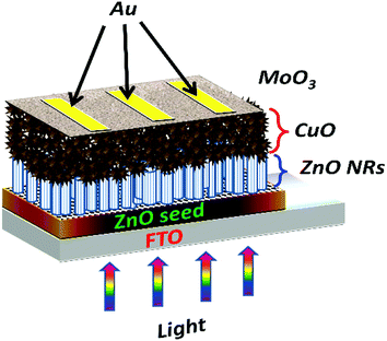 |
| | Fig. 1 Schematic design of ZnO/CuO/MoO3 heterojunction solar cell. | |
Morphological characterization of prepared ZnO nanorods, CuO nanostructures, and MoO3 layer was performed using by FEI Inspect S50 scanning electron microscope (SEM). Crystal structures were analyzed by the X-ray diffraction (XRD) technique using the Rigaku SmartLab X-ray diffractometer (CuKα radiation, λ = 1.54056 Å). Rietveld refinement was performed using the Rigaku PDXL-XRD analysis software. The absorption spectra were calculated by a VARIAN Cary 50 Scan UV-Vis spectrometer. The thickness of different nanostructured layers was measured using the n&k 1200 Analyzer. XPS spectra were acquired using a dual anode X-ray source, XR 04-548 (Physical Electronics), and an Omicron EA 125 hemispherical energy analyzer with a resolution of 0.02 eV in an ultra-high vacuum (UHV) chamber with a base pressure <10−10 torr. The X-ray source used was the Al-Kα source operated at 400 W and an X-rays incident angle of 54.7° and normal emission. Hall measurements were performed using MMR H-50 Hall, van der Pauw controller. The current–voltage (J–V) characteristics of the solar cells were measured by a Keithley 2450 source meter with AM 1.5 Global spectrum source for illumination. External quantum efficiency (EQE) spectra were measured using Oriel IQE 200 instruments. Capacitance measurements were performed using Agilent/HP 4274A multi-frequency LCR meter with external biasing. Impedance spectra were analyzed in the frequency range of 1 Hz to 10 MHz with 20 mV ac voltage using Omicron Bode 100 analyzer. EIS spectrum analyzer 1.0![[thin space (1/6-em)]](https://www.rsc.org/images/entities/char_2009.gif) 44 software was used to model the Cole–Cole plots obtained from the impedance measurements.
44 software was used to model the Cole–Cole plots obtained from the impedance measurements.
3. Result and discussion
3.1 Structural analysis
The crystal structure of ZnO nanorods was analyzed using X-ray diffraction (XRD) technique. Fig. 2(a–e) shows the XRD spectra of 0–20% cobalt-doped ZnO nanorods and corresponding Rietveld analysis (see Table S1†). All the peaks on X-ray diffraction patterns were well matched to the ZnO wurtzite-phase structure (JCPDS no. 36-1451).45 All the undoped and cobalt doped ZnO are highly c-axis oriented, and (002) diffraction peak position gradually shifted toward lower diffraction angle with higher cobalt doping. This indicates that the Co++ ions were well-substituted during doping into Zn sites without the creation of the secondary phase (within the detection limits). For 10%, 15%, and 20% cobalt doping, we observe an additional spinel ZnCo2O4 phase, which is a typically found spinel structure with Zn++ ions in the tetrahedral sites and Co3+ occupying the octahedral sites. In our previous studies,39 we have discussed the detail Rietveld analysis of these nanomaterials and found that the percentage of the wurtzite ZnO phase in samples decreases and the secondary phase of ZnCo2O4 increases with excessive cobalt concentration. However, for 10% cobalt doped samples, the existence of the ZnCo2O4 secondary phase is low (<5%) in comparison to other higher doped samples. Also, we observed that the crystallite size increases from 50.01 nm to 73.24 nm as cobalt doping is increased from 0 to 20%. The increase in crystallite size reveals the presence of cobalt in the ZnO lattice. During cobalt doping, distortion is produced by dopant atoms due to a mismatch between ionic radii of Zn++ and Co++. This mismatch created distortions at various locations across the ZnO lattice, and at higher cobalt concentrations, the distortion centers increase, which increases the average crystallite size.46 Fig. 2(f) displays the XRD spectra of the fabricated ZnO/CuO/MoO3 heterojunction solar cell. Diffraction peaks matching to the hexagonal wurtzite structure of ZnO (JCPDS no.36-1451)45 can be identified from the XRD plot. The intense (002) peak points out the crystalline nature of the ZnO nanorods, and it grows along the c-axis. Fig. 2(f) also shows the presence of the diffraction peaks, which belong to the monoclinic tenorite structure of CuO (JCPDS no. 48-1548).47 Previous reports48,49 have shown that CuO film deposited on ZnO film has peaks corresponding to (![[1 with combining macron]](https://www.rsc.org/images/entities/char_0031_0304.gif) 11), (111), and (
11), (111), and (![[2 with combining macron]](https://www.rsc.org/images/entities/char_0032_0304.gif) 02), which is consistent with our XRD results. XRD results confirm that there is no other secondary impurity crystalline phase (Cu or Cu2O or Cu(OH)2) in our device. Furthermore, the XRD patterns also show sharp diffraction peaks, which is consistent with the standard values of the orthorhombic MoO3 crystal structure (JCPDS card no. 76-1003).50,51
02), which is consistent with our XRD results. XRD results confirm that there is no other secondary impurity crystalline phase (Cu or Cu2O or Cu(OH)2) in our device. Furthermore, the XRD patterns also show sharp diffraction peaks, which is consistent with the standard values of the orthorhombic MoO3 crystal structure (JCPDS card no. 76-1003).50,51
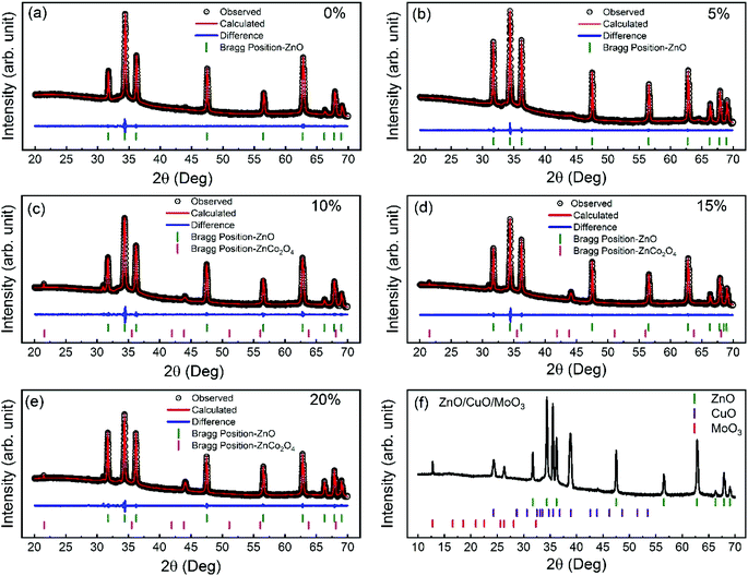 |
| | Fig. 2 XRD spectra and (a–e) Rietveld analysis of 0–20% cobalt doped ZnO nanorods (f) ZnO/CuO/MoO3 heterojunction solar cell. | |
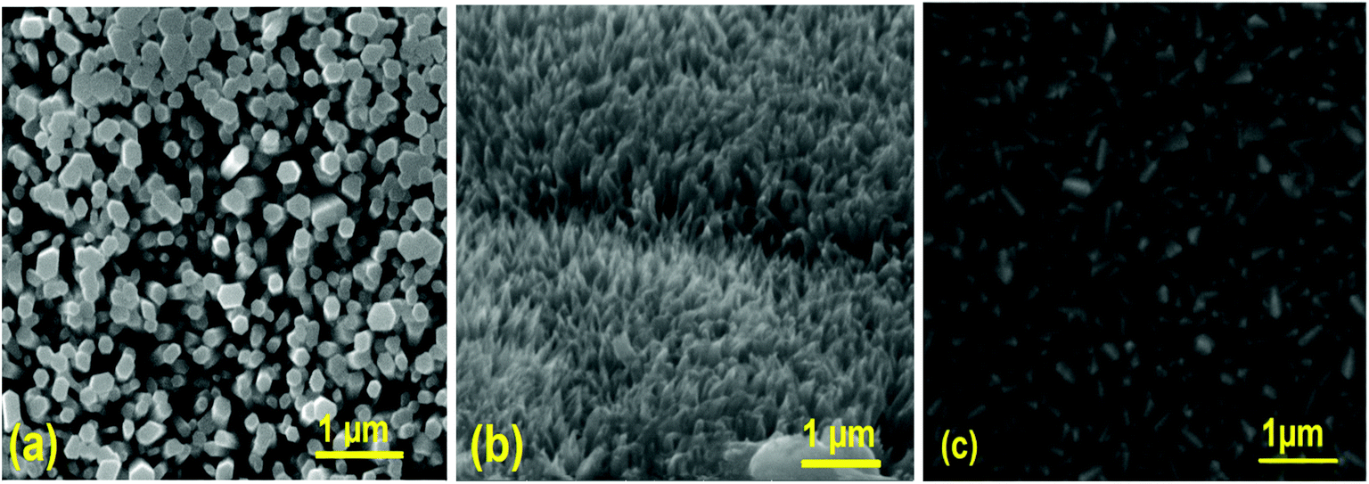
Fig. 3 shows a typical SEM image of ZnO nanorods, CuO nanostructures, and MoO3 thin film layers. From SEM images, we infer that ZnO has hexagonal shaped perpendicular aligned nanorods, and CuO has a unique cone-like nanostructure measuring less than 37 ± 5 nm. The average diameter of the undoped ZnO nanorods is about 94 ± 4 nm, and the length is about 453 ± 9 nm. The morphology and size of the prepared ZnO nanorods are well suited to act as a conducting path for electron and CuO nanostructures as light trapping centers, which can increase the rate of charge carrier generation.
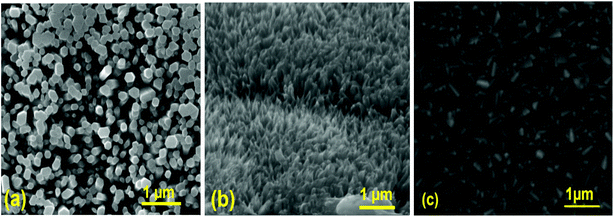 |
| | Fig. 3 SEM images of (a) undoped ZnO nanorods (b) CuO nanostructures (c) MoO3 thin film. | |
3.2 XPS analysis and band offsets
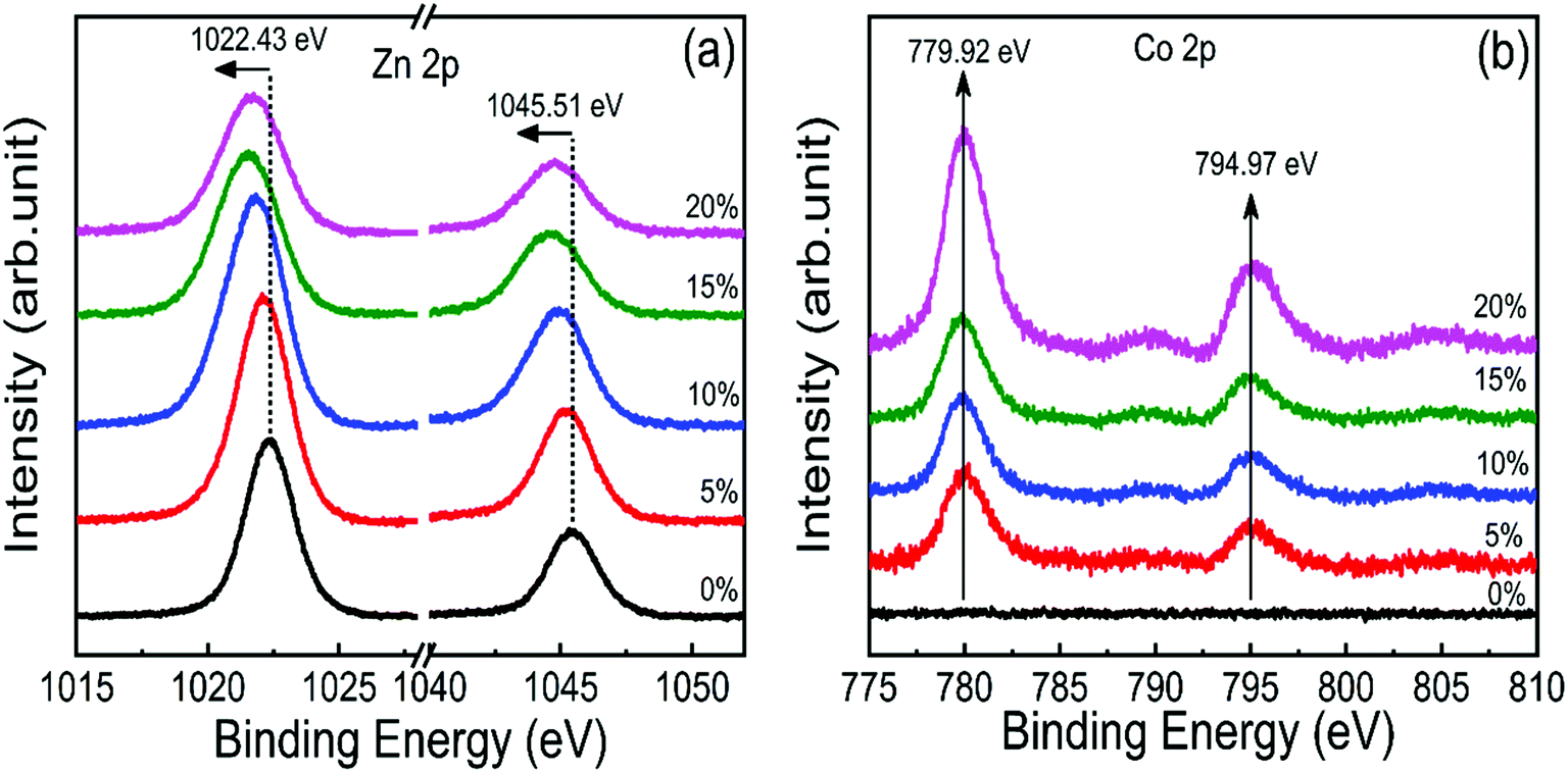
X-ray photoelectron spectroscopy (XPS) was performed to investigate the incorporation of cobalt in ZnO nanostructures. Fig. S2† shows the complete scan survey spectra of 10% cobalt doped ZnO/CuO heterojunction sample, which confirms the presence of Zn, Cu, Co, O, and C atoms in ZnO/CuO heterostructure. Also, a trace of the Sn atom is observed due to the FTO substrate. Fig. 4(a and b) displays the high resolution XPS core-level spectra of ZnO nanorods (Zn 2p and Co 2p) films with 0%, 5%, 10%, 15%, and 20% doping concentration. Characteristic binding energy peaks at 1022.43 eV and 1045.51 eV, assigned to Zn 2p3/2 and 2p1/2, were observed in all cobalt-doped ZnO spectra, as shown in Fig. 4(a), confirming the existence of divalent zinc ions in all samples.11 Spectra of the Co 2p core-level states as a function of cobalt concentration are displayed in Fig. 4(b), where Co 2p is observed at 780 eV and 795 eV with enhanced intensity and area, suggesting the incorporation of cobalt into the ZnO lattice. To investigate the incorporation of cobalt atoms into the ZnO host lattice structure, we deconvoluted the O 1s XPS spectra for all undoped and doped ZnO nanostructures into three different near Gaussian subpeaks shown in Fig. 5. The O 1s spectra of both the undoped and cobalt doped ZnO show the main peak (O 1s-Peak A), and two shoulder peaks (O 1s-Peak B and Peak C) centered at around 530.31 eV, 531.19 eV, and 532.52 eV respectively. The dominant peak at 530.31 eV (Peak-A) is attributed to O2− ions or oxygen atoms bonded with nearest neighbor metal ion species (Zn–O or Co–O) in a wurtzite structure and shows a very minor shift toward lower binding energy for doped samples.21,52 Peak-B is associated with O2− ions could reduce the oxygen vacancy concentration. By the cobalt doping process, strong and stable Co–O complexes are formed, thereby reducing oxygen-related defects, which in turn results in the selective passivation of deep level defects up to a certain doping level (in our case, 10% doping). This type of passivation of native defects of ZnO was observed in the previous study using Mg doping (up to 4%).53 Therefore, we can say that cobalt dopant can play a role in suppressing the formation of oxygen vacancies. Also, the weight (%) of the Peak-C in the O 1s spectrum in 10% cobalt doped ZnO is slightly smaller when compared to the corresponding peak area in the spectrum of undoped ZnO, which might be associated with a reduction in the concentration of hydroxyl groups in the ZnO due to cobalt doping.21 However, the weight (%) of the Peak-C is slightly enhanced with higher cobalt dopant (15% and 20%) due to cobalt clustering.
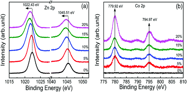 |
| | Fig. 4 High-resolution core-level XPS spectra of (a) Zn 2p and (b) Co 2p state in 0–20% cobalt ZnO nanorods. | |
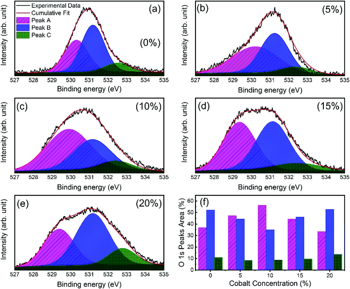 |
| | Fig. 5 Core level XPS spectra of O 1s state in (a) undoped (b–e) 5–20% cobalt doped ZnO nanorods. The XPS oxygen peaks were deconvoluted to three different near-Gaussian subpeaks named as Peak A, Peak B, and Peak C. (f) Relative weight percentage of O 1s peaks as a function of cobalt concentration. | |
Similarly, the high-resolution XPS spectra of Cu 2p states are shown in Fig. 6. The core-level spectra were fitted with Pseudo-Voigt (mixed Lorentzian–Gaussian) function by employing a Shirley background correction. Peaks around at 933.98 eV and 953.86 eV were observed, which are assigned to the Cu 2p3/2 and Cu 2p1/2 state in CuO.23 In addition to the main peak, the strong shake-up satellite peaks are also detected at the higher binding energy (BE) side, at 941.28 eV, 943.67 eV, and 962.33 eV, which are characteristics of partially filled d-block (3d9) of Cu++ ions.49 The peak positions and presence of the shake-up satellites indicate the formation of pure CuO, which is supported by our XRD results. Also, the position of the Cu 2p peaks in ZnO/CuO heterojunction samples shifts to higher binding energy compared to pure CuO nanostructures. The shift of Cu 2p peaks to higher binding energy can be explained by the strong interaction between ZnO and CuO nanostructures in our heterojunction.49 Similar results have been reported earlier by the researcher while performing XPS studies of ZnO/CuO nanostructures by different (RF sputtering, hydrothermal, electrospinning) routes.9,13,49
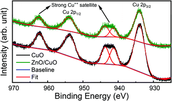 |
| | Fig. 6 High-resolution XPS spectra of Cu 2p state in pure CuO nanostructures (black) and ZnO/CuO heterojunction (green). | |
The critical parameters leading restrictions for the performance of the photovoltaic cells is band offsets at the heterojunction interface. Depending on the band offsets present at any heterojunction solar cells, the charge transport across the junction interface is affected.54 To determine band offsets and to explain the structure of ZnO/CuO heterojunction, valence band offset (VBO) was measured by calculating the binding energy difference between valence band maximum (VBM) and the core level (CL) using XPS analysis.26 Fig. S3† shows the valence band (VB) spectrum of undoped and cobalt doped ZnO along with CuO nanostructures, and the valence band maximum (VBM) value of 2.64 eV–1.80 eV and 0.57 eV are extrapolated by linear fitting for 0–20% cobalt doped ZnO and CuO, respectively. For the calculation of VBO, we use the core-level measurement technique, as proposed by Kraut et al.55 In this method, the VBO of ZnO/CuO interface can be calculated using the following equation:
| | |
ΔEVBO = [EZnO/CuOZn 2p − EZnO/CuOCu 2p] − {[EZnOZn 2p − EZnOVBM] − [ECuOCu 2p − ECuOVBM]};
| (1) |
where
Esi denotes the binding energy of the core level i for the sample s while
EsVBM denotes the VBM for the sample s. Further, conduction band offset (CBO) was calculated by using bandgap values of ZnO, CuO, and the VBO by the following relation:
54| | |
ΔECBO = EZnOg − ECuOg − ΔEVBO;
| (2) |
where
EZnOg and
ECuOg are the bandgap of ZnO and CuO calculated by the Tauc plot using absorption spectra (see Fig. S4
†).
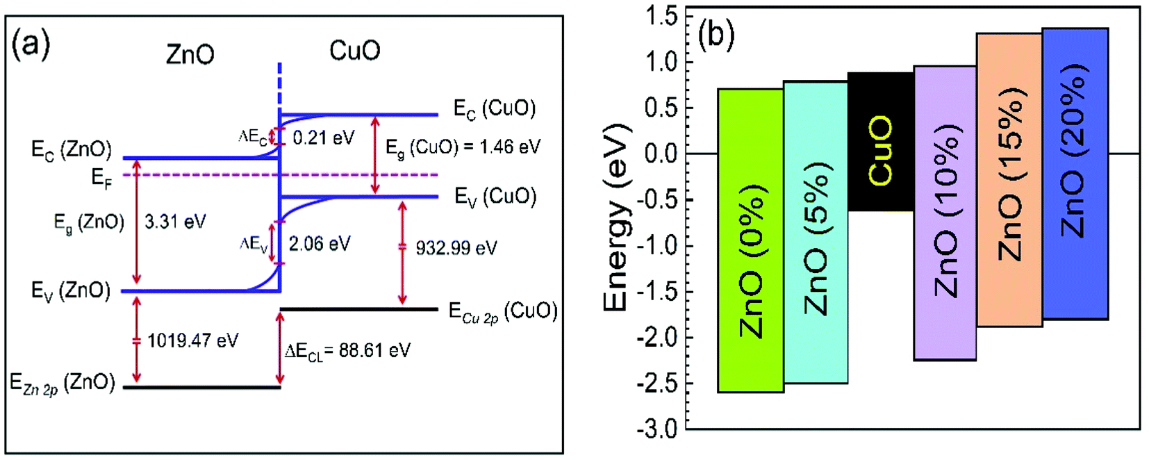
The calculated values for VBO and CBO are shown in Table 1. Similar results (VBO = 2.83 eV and CBO = −0.73 eV) were obtained by Hussain et al.13 for undoped ZnO/CuO nanocomposite. As the cobalt doping level was below 10%, the conduction band of ZnO was lower than that of the CuO nanostructures; i.e., the value of CBO was negative, thus forming a cliff structure at the interface with type-II band alignment.21,54 When the cobalt doping concentration was above 10%, the conduction band of ZnO was higher than that of the CuO; i.e., the CBO was positive, thus forming a spike structure with type-I band alignment. Many previous studies54,56–58 showed that a large negative CBO increases the probability of recombination at the interface, and large positive CBO produces a barrier, which hinders the collection of photogenerated carriers. Accordingly, a small positive CBO with a notch like structure at the junction is necessary for stronger band bending to prevent the injected electrons from going to the junction and decrease the chances of recombination. We calculated a positive CBO of 0.07 eV for a 10% cobalt doped ZnO/CuO device (Fig. 7). For 15% and 20% cobalt doped ZnO heterojunctions, where the CBO spike is higher (0.4 eV), and as a result, the recombination became faster again. This consequence might be due to the increase in the trap density because of excessive cobalt doping, and this creates the negative effect of the trap states on the recombination mechanism despite the positive effect of the notch or spike-like structure.
Table 1 Bandgap, VBO, and CBO of 0–20% cobalt doped ZnO/CuO heterojunction solar cells
| Co% |
Bandgap ZnO (eV) |
Bandgap CuO (eV) |
ΔEV (eV) |
ΔEC (eV) |
| 0 |
3.31 |
1.46 |
2.06 |
−0.21 |
| 5 |
3.28 |
1.93 |
−0.11 |
| 10 |
3.22 |
1.69 |
0.07 |
| 15 |
3.20 |
1.31 |
0.43 |
| 20 |
3.17 |
1.23 |
0.48 |
 |
| | Fig. 7 (a) Band diagram of 0% cobalt doped ZnO/CuO heterojunction solar cells. (b) Schematic band offsets in 0–20% cobalt doped ZnO/CuO heterojunction. VBM and CBM values are from the Fermi level. | |
3.3 Conductivity and Hall measurements
It is well known that the electrical properties of the interfacial layers are essential for the performance of the solar cell devices because they will affect charge transport at the interface.59 Fig. 8(a) shows the conductivity of 0–20% cobalt doped ZnO nanostructures. The electrical conductivity increases with increasing cobalt concentration and shows a maximum value of 20.55 Ω−1 cm−1 at a 10% cobalt doping level, but beyond this doping concentration, the conductivity was found to decrease again. At relatively lower doping concentrations (≤10%), electrons from the dopant play a dominant role in the film and as less oxygen vacancy scattering occurs, the conductivity increases.25,59 At a higher cobalt doping concentration of above 10%, the disorder produced in the lattice (due to cobalt clustering) increases the efficiency of scattering mechanisms such as phonon scattering and ionized impurity scattering which, in turn, causes a decrease in conductivity.60 ZnO with higher conductivity is beneficial for reducing the ohmic voltage loss when electron transport within the layer, resulting in the enhancement in VOC and FF of the solar cell which will be discussed later. Hall measurement shows the n-type conductivity in all undoped and doped ZnO samples. We observed that the carrier concentration and mobility of cobalt doped ZnO films increases to 3.18 × 1018 cm−3 and 40.41 cm2 V−1 s−1, a peak value for the 10% cobalt doped sample. However, after 10% cobalt doping level, mobility starts to decrease, whereas carrier concentration becomes saturated. This can be explained as due to excessive cobalt doping; more defects will be formed and acts as scattering centers, which results in the formation of sites capable of trapping carriers. After trapping the charge carriers, the traps became electrically charged, creating a potential energy barrier, which hindered the transport of photogenerated carriers from one crystallite site to another, thereby reducing their mobility and conductivity.61,62 A similar result was obtained by Wu et al.63 for 0–10% cobalt doped ZnO and proposed that the substitution of Co++ for Zn++ could improve the electrical conductivity and mobility up to certain limit due to the increase in carrier concentration. The increased mobility resulting from increasing the cobalt doping also ensures that electrons can quickly transport to the FTO electrode. Hall measurement on CuO films shows p-type conductivity with a carrier concentration of 2.93 × 1016 cm−3, mobility of 0.74 cm2 V−1 s−1, and conductivity of 3.46 × 10⁻³ Ω−1 cm−1.
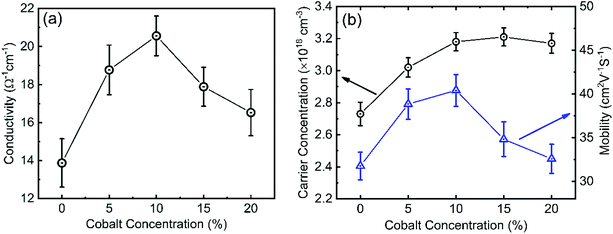 |
| | Fig. 8 (a) Conductivity (b) mobility and carrier concentration of 0–20% cobalt doped ZnO. | |
3.4 I–V and EQE analysis
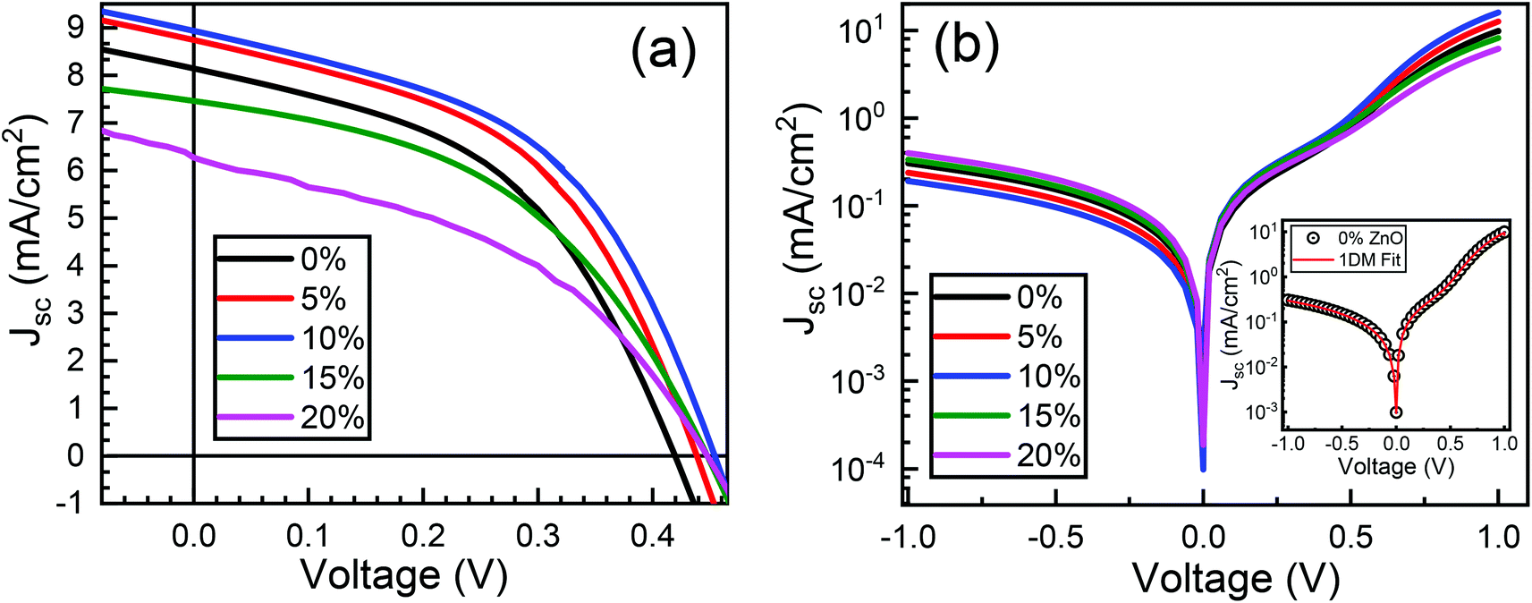
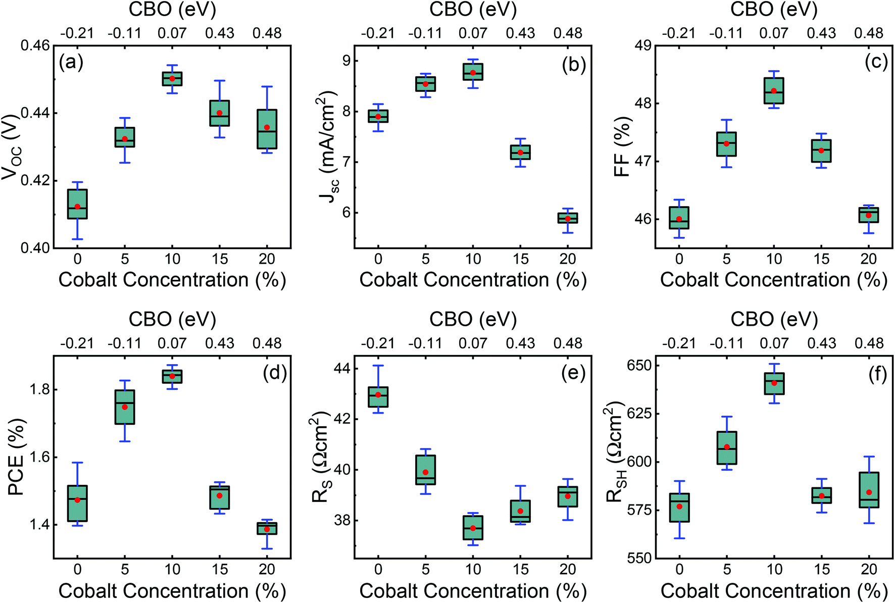
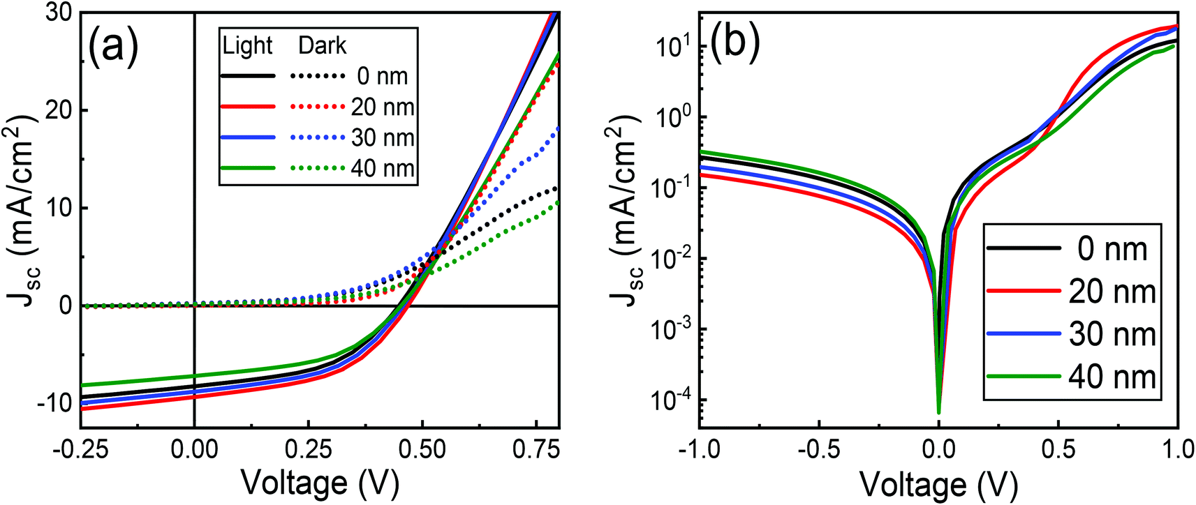
Typical current density–voltage (J–V) characteristics of cobalt doped ZnO/CuO heterojunction solar cell (champion cell) under standard AM1.5G illumination are displayed in Fig. 9(a). To assure credible device performance, the statistical parameter distribution of eight devices were plotted in Fig. 10. Since statistical deviations are relatively small; thus, the device improvement is reliable. The CBOs were varied in the range from −0.21 to 0.48 eV with cobalt doping. As expected, a significant improvement in open-circuit voltage was observed when a spike structure was formed at the junction interface corresponding to 10% cobalt doping. When the positive CBO was very high (0.4 eV), the VOC is slightly reduced. Likewise, the short-circuit current density (JSC) and the fill factor (FF) of the heterojunction solar cell first increase with changing CBO (from −0.21 eV to 0.07 eV) and then decrease when the CBO is large enough (0.4 eV). The solar cell with 10% cobalt-doped ZnO exhibited the best performance, with an average power conversion efficiency of 1.87%, VOC of 0.45 V, JSC of 9.17 mA cm−2, and FF of 48.22% (Table S2†). All these values are higher than those solar cells based on undoped ZnO and CuO. However, a decrease in photocurrent is observed due to the large spike for a conduction band offset greater than 0.11 eV (15% and 20% cobalt doped). The current–voltage results revealed that the performances of ZnO/CuO heterojunction extremely depend on the doping concentration of cobalt in ZnO nanorods and their band alignments.
 |
| | Fig. 9 (a) I–V characteristics under light and (b) dark IV characteristics of 0–20% cobalt doped ZnO/CuO heterojunction solar cells. The insets of (b) show one diode model fit of 0% ZnO/CuO solar cell. | |
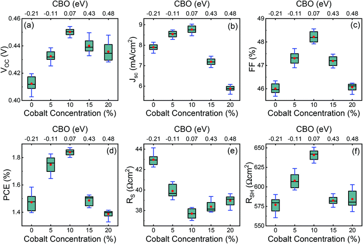 |
| | Fig. 10 Statistics of device performance using various cobalt doped ZnO window layer (0–20%). (a) Open circuit voltage (VOC), (b) short circuit current density (JSC), (c) fill factor (FF), (d) power conversion efficiency (PCE), (e) series resistance (RS), and (f) shunt resistance (RSH). The solid red circle represents the average values, and the horizontal lines in the box denote the 25th, 50th, and 75th percentile values. | |
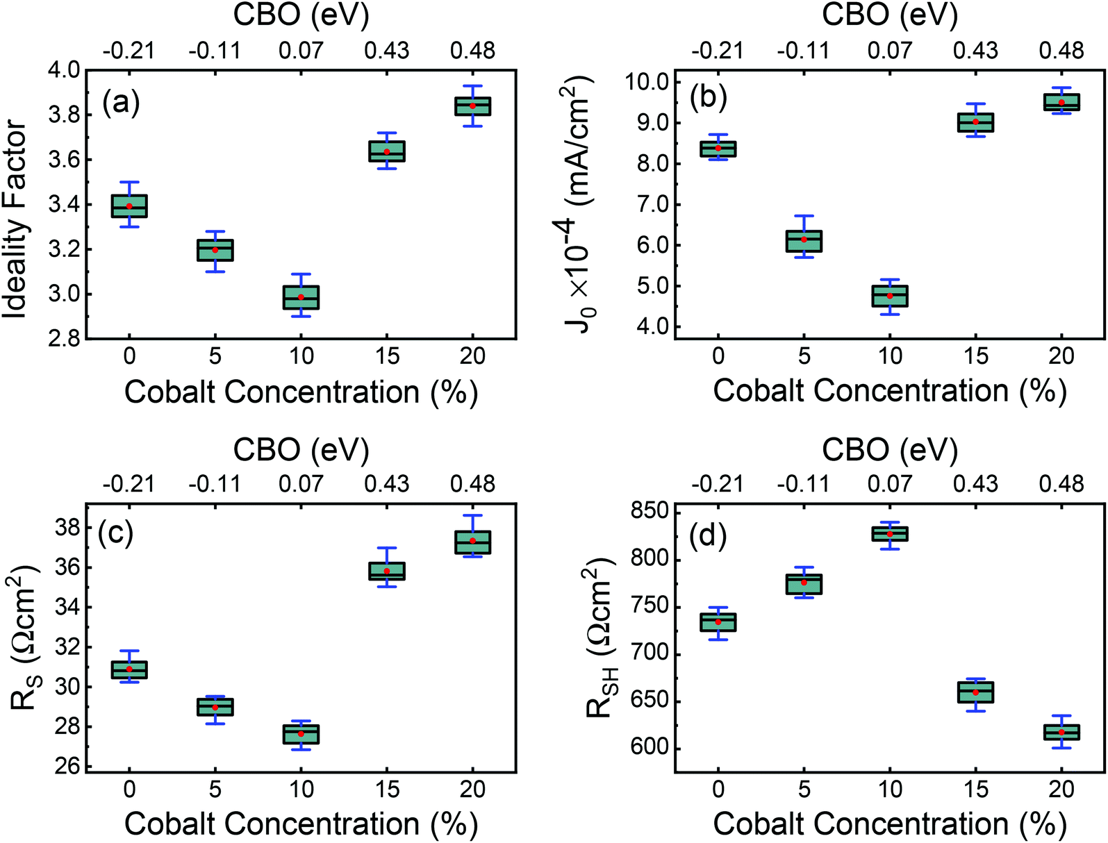
To find out the effect of cobalt doping in ZnO/CuO heterojunction on charge recombination mechanism, the diode formation of the solar cells was studied by examining the dark J–V characteristics. The diode parameters in the solar cells, such as the ideality factor (n) and reverse saturation current density (J0), are important indicators of the dominant recombination mechanism. The dark J–V plot (Fig. 9(b)) reassures that the ZnO/CuO heterojunction display rectifying performance, which proves the p–n junction formation. Fig. 9(b) shows the semi-log J–V plot, and the inset shows experimental dark J–V data (0% cobalt) fitted with a generalized single diode Shockley equation.64
| |
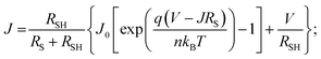 | (3) |
where
J0,
n,
RSH,
RS,
q,
kB, and
T are the reverse saturation current density, the diode ideality factor, the shunt resistance, the series resistance, the electronic charge, the Boltzmann constant, and the temperature of the device, respectively. Fitted parameters extracted from the single diode Shockley equation are displayed in
Fig. 11 (see Table S3
† for average value). For undoped ZnO, average reverse saturation current density, series resistance, shunt resistance, and diode ideality factor of 8.38 × 10
−4 mA cm
−2, 30.88 Ω cm
2, 736.4 Ω cm
2, and 3.39 respectively, were obtained. This high reverse leakage current is the indication of the existence of significant interface defects and non-radiative recombination at the ZnO/CuO junction. Also, the high value of leakage current is responsible for the limitation of open-circuit voltage
65,66 as well as the fill factor of the device, which can be seen on our device performances. As seen in
Fig. 11, the dark reverse leakage current of the ZnO/CuO heterojunction decreased with increasing cobalt doping level-up to 10%, indicating a suppressed recombination. The continuous decrease in the dark current of the solar cells may be due to the increased built-in potential (explained later in
C–
V analysis) in the cobalt doped ZnO layer, attributed to the increased Femi level of cobalt-doped ZnO.
67 In our case, the ideality factor is higher than 2, and it is reported that if the ideality factor is higher than 2, the defect activities are supposed to be dominated by a recombination process with traps distributed at the interface and surface.
66,68 Besides, the inhomogeneous thickness of ZnO nanorods and non-uniformity of interfacial charges could contribute to the high ideality factor. Since the existence of vacancies and mid-gap trap states associated with nonidealities in both ZnO and CuO surface also forms a substantial number of interfacial states at the ZnO/CuO junction.
38 These nonidealities might be responsible for defect-mediated tunneling,
69,70 which stimulate photogenerated carrier in the reverse direction. The tunneling process mediated by defect densities could cause shunting of the device and result in a lower reverse breakdown voltage.
39 This type of behavior can be seen in
Fig. 9 with sizeable reverse leakage current and low photocurrent. The average value of the ideality factor first reduced from 3.39 to 2.98 as the cobalt content was increased to 10% and then increased to 3.84, with a further increase in cobalt concentration. The 10% cobalt-doped device exhibits the smallest diode ideality factor, indicating that this device shows the best suppression of interfacial recombination, which might be due to a small positive CBO, increased built-in potential and suitable structural properties such as lesser defect density. However, even for the 10% cobalt doped cells, the ideality factor is still high. This substantial value indicates that the space-charge recombination still dominates the device loss mechanism.
 |
| | Fig. 11 Statistics of the result obtained from one diode model fitting of dark J–V characteristics of various cobalt doped ZnO layer (0–20%). (a) Ideality factor (n), (b) reverse saturation current density (J0), (c) series resistance (RS), and (d) shunt resistance (RSH). The solid red circle represents the average values, and the horizontal lines in the box denote the 25th, 50th, and 75th percentile values. | |
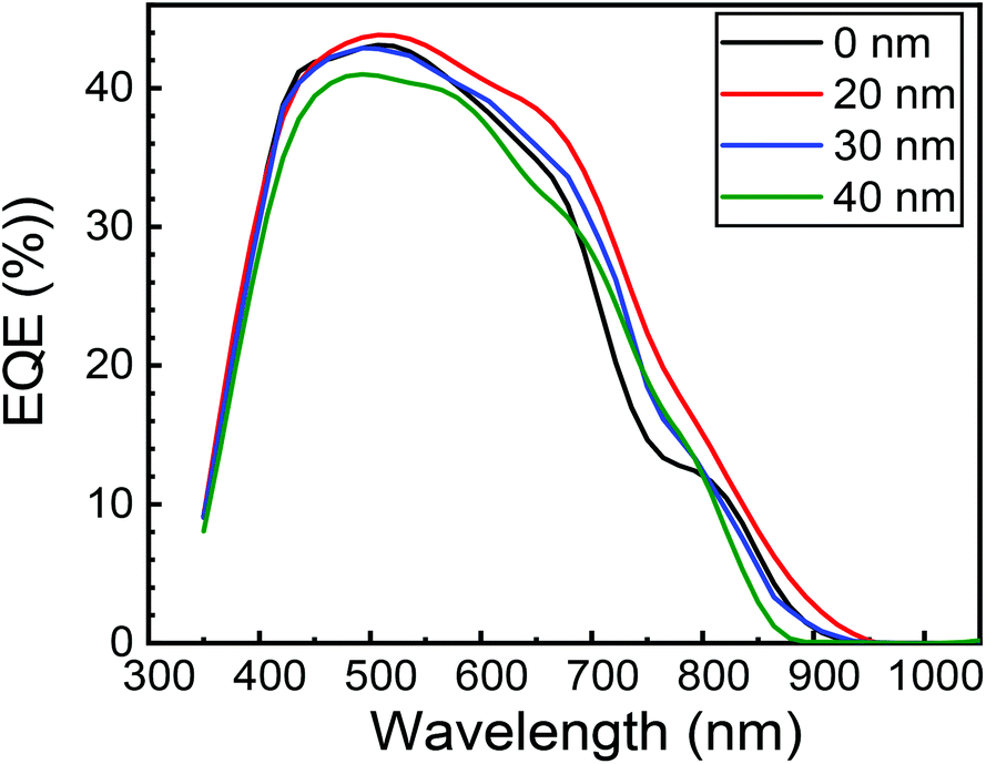
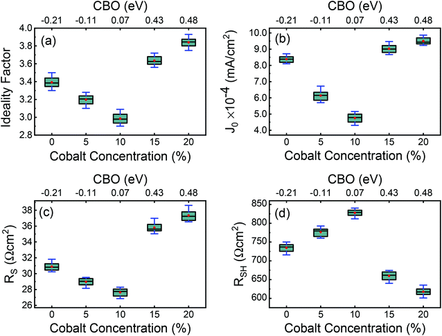
Fig. 12 shows the external quantum efficiency (EQE) of typical ZnO/CuO heterojunction solar cells with the best PCE at each cobalt content (0–20%). By integrating EQE spectra with the standard solar spectrum, we found the calculated JSC values of around 8.52, 8.96, 9.12, 7.96, and 6.68 mA cm−2, respectively, for 0–20% cobalt doped ZnO. These JSC values from EQE agrees with those obtained from the J–V analysis. We can observe poor EQE in the long-wavelength region (>550 nm), meaning a poor carrier collection in this region, which explains its lower short circuit current density (JSC). This indicates the loss of deeply absorbed photons due to recombination in the bulk and depletion regions of the device.66 In the wavelength range corresponding to the ZnO layer absorption, the EQE of the doped cell is slightly inferior to the cell with the un-doped absorber layer. Also, the EQE results show slight band tailing, which is attributed to defect complexes present in the CuO layer.71,72 However, the increase in EQE (from 38% to 43%) with 10% cobalt doped ZnO likely results from the factors such as improvement in conduction band offsets and hence better charge collection efficiency due to the reduction in interface recombination. Thus, further improvement in solar cells should focus on the enhancement of the heterojunction interface and conduction band alignment to improve the VOC by doping of the CuO absorber layer as well.
 |
| | Fig. 12 The external quantum efficiency of 0–20% cobalt-doped ZnO/CuO heterojunction solar cells. | |
3.5 Impedance and capacitance–voltage (CV) analysis
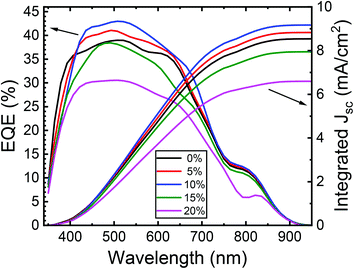
To gain information about the carrier recombination process, we investigated ZnO/CuO devices using impedance spectroscopy. Fig. 13 displays the impedance spectrum of devices in dark conditions. The impedance patterns of different undoped and cobalt doped samples analyzed were fitted using an equivalent circuit model shown in the inset of Fig. 13(a). The Cole–Cole plot reveals two distinct features, that is, a small arc at high frequency and a large arc at low frequency. Here, the high-frequency feature (Fig. 13(b)) is ascribed to charge transfer process, while the lower frequency element contains the information about carrier recombination process.73–76 In addition, the value of the starting point at the real part of the Cole–Cole plot corresponds to the series resistance RS.22 In our devices; the RS is related to the resistance, including that arising from external wires or the substrates. In the equivalent circuit, the resistance, Rct, known as charge transfer resistance, is associated with the ZnO/CuO interface or the CuO/Au contact and the selective contact capacitance (CPEct) owing to the charge buildup at the interfaces. Whereas, the element Rrec and CPEμ are associated with recombination resistance and chemical capacitance of the system. The fitted parameters based on the equivalent circuit are listed in Table 2. In the equivalent circuit, the constant phase element (CPE) accounts for the deviation of the capacitance from an ideal capacitor since several theories such as leaky-capacitor and non-uniform current distribution have been proposed to account for the non-ideal behavior of capacitance such as surface roughness, porosity, and various surface states.77–79 We also observed that CPEct is lowest for 10% cobalt-doped sample, which implies less charge accumulation and efficient charge transport by 10% cobalt doped ZnO layer. Since CPEct is related to charge collection at the interfaces, having a small value is favorable for increased device performance.80 We observed that the 10% cobalt-doped ZnO based device gives the lowest Rct value (573.09 Ω), indicating that charge extraction is most efficient at the interface of this sample compared to all the investigated samples, a result that is consistent with the conductivity and electron mobility values. The lower Rct values must contribute to the highest JSC value of a 10% cobalt-doped device.75,81 In contrast, when various cobalt concentrations were introduced into ZnO nanostructures, the Rrec is significantly increased from 6582 Ω for the cell with pristine ZnO to 7973 Ω corresponding to the cells with 10% Co-doped ZnO, respectively. The much larger Rrec for the device with Co:ZnO prepared with the cobalt concentration of 10% originates from fewer defect-assisted traps, indicating effective suppression of the charge recombination and leakage current.73 Furthermore, due to the more favorable band alignments between the 10% cobalt doped ZnO and CuO, previously discussed in XPS analysis, the extraction of charge carrier is energetically favored and thus decreased interfacial charge accumulation occurs, resulting in a decrease in carrier recombination in the ZnO/CuO interface. This is consistent with the increase in Rrec observed in all (8 samples for each doping level) 0–20% cobalt doped devices, which denotes less frequent recombination events. Higher recombination resistance value (Rrec) of 10% cobalt doped sample from impedance analysis also confirms its more substantial shunt resistance (RSH) from J–V measurement, suggesting that the charge recombination is unfavorable between the interface of ZnO and CuO layer. This result shows a clear correlation between a higher Rrec (lower recombination rate) and a higher VOC of the device. In other words, the samples with cobalt doping (up to 10%) reveals that the presence of cobalt in ZnO lattice induces a decrease in the recombination rate, thus enhancing the VOC of the devices and solar cell performances. This effect is reversed when the cobalt doping increases beyond 10%. This consequence might be due to the increase in the deep level trap density and higher conduction band offsets because of excessive cobalt doping.
 |
| | Fig. 13 Cole–Cole plots of the 0–20% cobalt doped ZnO/CuO heterojunction solar cells. Insets indicate the equivalent circuit model. (b) Magnified view of Cole–Cole plots in the high-frequency region. | |
Table 2 Parameters extracted from impedance circuit fitting of 0–20% cobalt doped ZnO/CuO heterojunction devices
| Cobalt% |
Rs (Ω) |
Rtr (kΩ) |
Rrec (Ω) |
CPEtr (nF) |
n1 |
CPEμ (nF) |
n2 |
Ctr (nF) |
Cμ (nF) |
τ = RrecCμ (μS) |
τ(Cole–Cole) (μS) |
| 0 |
18.2 |
1.24 |
6.58 |
13.1 |
0.910 |
24.1 |
0.87 |
4.39 |
6.52 |
42.9 |
44.2 |
| 5 |
17.8 |
0.885 |
7.34 |
14.6 |
0.890 |
20.5 |
0.89 |
3.63 |
6.91 |
50.7 |
51.6 |
| 10 |
17.4 |
0.573 |
7.97 |
14.5 |
0.870 |
19.3 |
0.90 |
2.52 |
7.28 |
58.0 |
60.2 |
| 15 |
17.0 |
1.31 |
6.38 |
19.2 |
0.890 |
20.9 |
0.88 |
5.19 |
6.19 |
39.5 |
37.9 |
| 20 |
17.9 |
1.59 |
5.68 |
19.8 |
0.890 |
22.7 |
0.87 |
5.50 |
5.95 |
33.8 |
32.5 |
From the complex impedance spectrum, the effective carrier lifetime can be estimated since the peak of the large semicircle in the Cole–Cole plot corresponds to a frequency whose reciprocal is the effective carrier lifetime.82,83 Carrier lifetime calculated from the peak of the large semicircle in a Cole–Cole plot and RC time constant (τ = RrecCμ) using equivalent circuit fit is within 4% (Table 2). For the undoped device, the effective carrier lifetime is determined to be 44.2 μs, and the corresponding values for doped samples (5–20%) are 51.6, 60.2, 37.9, and 32.5 μs, respectively. The longer carrier lifetime of the device indicates that photogenerated carriers have more time to move toward, and ultimately be collected by the electrode without suffering recombination.82 We can say that the device with 10% cobalt doped samples undergoes less recombination since it has a long carrier lifetime of 60.21 μs. This is consistent with the more considerable recombination resistance of the device (the diameter of the large semicircle), which indicates less carrier recombination inside the device. The longer carrier lifetime and larger recombination resistance should be induced by the reduction of defects as well as the improved band alignment between ZnO and CuO layers by cobalt doping.
To investigate more into the recombination phenomena, we have characterized the capacitive spectra. Mott–Schottky analysis is commonly used to determine a semiconductor's doping density and the built-in bias potential.84 Depletion width and the capacitance–voltage behavior is then expressed according to the Mott–Schottky equation as
| |
 | (4) |
| |
 | (5) |
where
C represents the depletion capacitance,
Vbi is the built-in potential,
V is the applied bias,
A is the device area (0.16 cm
2),
ε is the active layer's dielectric constant (dielectric constant of 18.1 was assumed for CuO
85),
ε0 is the permittivity of free space, q is the electronic charge,
w is the depletion width, and
Na is the background doping concentration. The built-in potential and doping density are then found by fitting
eqn (4) to the linear portion of the
C−2 versus bias voltage plot, where the slope gave the background doping density and extrapolated intersection with the voltage axis gives the built-in potential (
Fig. 14).
84 Modulating frequency of 1 kHz is used for
C–
V measurements because, at high frequency, not all of the defect states can respond to the modulating signal and hence no longer contribute to the junction capacitance.
86 Therefore, low-frequency measurements provide a more reliable description of the carrier dynamics in the system, despite the role of traps and defects.
 |
| | Fig. 14 (a) Capacitance–voltage (C–V) and Mott–Schottky plots of the 0–20% cobalt doped ZnO/CuO heterojunction solar cells. Variation in (b) built-in potential, (c) background doping concentration, and (d) depletion width as a function of cobalt concentration. | |
The effect of cobalt doping on built-in potential, depletion width, and background doping concentration are shown in Fig. 14(b–d). In the case of the undoped sample, a narrow depletion width of 174 nm, a built-in potential of 0.514 V, and a background doping concentration of 3.41 × 1016 cm−3 was observed. This value of background concentration in ZnO/CuO heterojunction is comparable to the result (3× 1016 cm−3) obtained by Chabane et al.11 This result shows that the high background doping concentration in our sample is consistent with small depletion width, which will increase the probability of recombination. As the cobalt concentration is increased to 10%, the corresponding depletion width and built-in potential become 227 nm and 0.611 V, respectively, and the background doping concentration reduces to 2.37 × 1016 cm−3. This result indicates that the solar cell is not still fully depleted and could be the reason for low device performance arising from low carrier collection. However, this study demonstrates the effectiveness of cobalt doping on enhancing the depletion width and built-in potential. This improved performance can be seen in the EQE and J–V plot due to the broader depletion width provided by the low background doping density. Here, the net effect of these processes is also directly observed in the properties of the built-in voltage. The high initial background doping level evident in solar cells is due to defects forming from the low-temperature growth conditions because there exist many defects (oxygen vacancies or interstitials) in the nanostructured films grown by a chemical bath deposition process. By the cobalt doping process, strong and stable Co–O complexes are formed, thereby reducing oxygen-related defects (can be seen in O 1s spectra in XPS analysis); this results in the selective passivation of deep level defects up to certain doping level (in our case 10% doping).53
3.6 Effect of MoO3 buffer layer
Fig. 15 shows IV characteristics of 10% cobalt doped ZnO/CuO/MoO3 heterojunction solar cells for a 0–40 nm thick MoO3 layer. A cross-over in the forward-bias (V > 0.5 V) region is observed for the device without any MoO3 buffer layer. This type of cross-over is an indication of the presence of a Schottky barrier at the CuO/Au contact in opposition to the junction formed at the ZnO/CuO interface.87 Such a Schottky barrier would obstruct the extraction of holes from the CuO layer, regulating both the dark and the photocurrent, and dropping the open-circuit voltage,38 as is observed in Fig. 15(a). The incorporation of MoO3 between the CuO and Au electrode reduces this cross-over effect, concurrently increasing all the parameters. It is to be noted that the PCE increases firstly and then decreases with the increase of MoO3 thickness and achieves its highest value of 2.11% when the MoO3 thickness equals to 20 nm (Table 3). Further increase in the thickness of MoO3 deteriorates the performance of solar cells. It is evident that the thickness of the MoO3 buffer layer can significantly affect the solar cell parameters of JSC, VOC, and FF and then lead to the variation of power conversion efficiency. The increase of JSC and FF might be attributed to smaller series resistances and lower recombination rates as the MoO3 thickness increases from 0 to 20 nm; while the decrease of JSC and FF as the MoO3 thickness further increases to 30 nm and 40 nm should be due to more significant series resistances and higher recombination rates induced by thick MoO3 layers. It is worth pointing out that VOC keeps increasing when the MoO3 thickness is varied from 0 to 20 nm (Table 3). If MoO3 thickness increases beyond 20 nm, the VOC decreased gradually due to electron–hole recombination induced by charge accumulation emerging at the interface between MoO3 and CuO layer.88 This hypothesis is verified by our impedance analysis results (Table S4†), where we observed charge transfer resistance is decreased, and recombination resistance is slightly increased by 20 nm thick MoO3 layers. Furthermore, a decrease in charge transfer capacitance is observed, which again confirms the reduced charge accumulation and increased charge extraction by optimized MoO3 thickness.
 |
| | Fig. 15 (a) I–V characteristics under light and dark of 10% cobalt doped ZnO/CuO/MoO3 heterojunction solar cells with a different thickness of the MoO3 buffer layer. (b) Semi-log plot of dark IV for one diode model fit. | |
Table 3 Average photovoltaic parameters of 10% cobalt doped ZnO/CuO/MoO3 heterojunction devices for 0–40 nm thick MoO3 buffer layer
| MoO3 (nm) |
VOC (V) |
JSC (mA cm−2) |
FF (%) |
η (%) |
RS (Ω cm2) |
RSH (Ω cm2) |
n |
J0 × 10−4 (mA cm−2) |
| 0 |
0.4544 ± 0.0075 |
9.174 ± 0.2060 |
48.22 ± 0.2446 |
1.870 ± 0.0246 |
37.69 ± 0.5012 |
641.0 ± 7.212 |
2.986 ± 0.0657 |
4.754 ± 0.3038 |
| 20 |
0.4680 ± 0.0067 |
9.495 ± 0.1784 |
48.43 ± 0.2823 |
2.112 ± 0.0527 |
35.28 ± 0.6762 |
717.6 ± 8.859 |
2.497 ± 0.0528 |
0.939 ± 0.2984 |
| 30 |
0.4573 ± 0.0084 |
9.234 ± 0.2153 |
48.27 ± 0.2308 |
1.897 ± 0.0259 |
37.18 ± 0.5539 |
663.4 ± 9.703 |
2.751 ± 0.0726 |
4.613 ± 0.3274 |
| 40 |
0.4531 ± 0.0078 |
8.050 ± 0.3889 |
47.36 ± 0.3185 |
1.569 ± 0.0402 |
38.57 ± 0.5527 |
593.9 ± 10.01 |
3.094 ± 0.0688 |
8.372 ± 0.3106 |
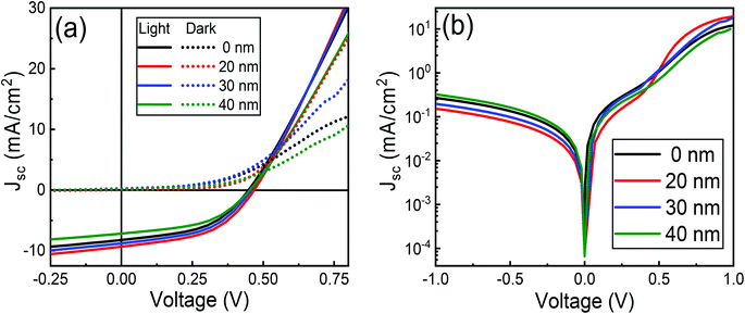
The effect of the MoO3 buffer layer is also evident in dark J–V characteristics (Fig. 15(b)). A reduction in diode ideality factor to 2.50 is observed with a 20 nm thick MoO3 layer, which means electron–hole recombination is reduced due to better ohmic contact. Besides, smaller ideality factor (2.50) achieved for MoO3-based devices also proves the better hole-selectivity, which results in decreased charge recombination loss at the CuO/Au interface. Subsequently, with MoO3 thickness' continuous increasing from 20 nm to 40 nm, the ideality factor rises from 2.50 to 3.09 attributed to charge accumulation, which leads to enhanced recombination. The optimum efficiency can be obtained for the device with a 20 nm MoO3 layer and a minimum ideality factor (2.50), which indicates that the carrier recombination decreased to the minimum. Therefore, the variation of circuit parameters could be attributed to charge accumulation at the CuO/Au Schottky type contact or CuO/thick-MoO3 interface. The lower J0 (9.39 × 10⁻⁵ mA cm−2) of the 20 nm thick MoO3 device compared to the current density without MoO3 device affirms that reduced recombination is achieved in the former device. This is an indication that an increased hole extraction efficiency is due to the decrease in the height of the Schottky barrier.38 The dark J–V characteristics show that the MoO3-based device possesses better diode behavior with lower leakage current density and higher rectification ratio than that of the device without MoO3. This implies that the MoO3-based PV cells maintain smaller reverse saturation current (J0) and ideality factor (n), which are the significant parameters contributing to the suppression of electron–hole recombination. While the MoO3 buffer layer is thick >20 nm, the charge extraction will be hindered; the photo-generated charges would be recombined in the buffer layer and degrade the solar cell performance. This type of effect is also discussed with reports of enhanced hole injection into organic hole-transport layers upon the insertion of a MoO3 buffer layer.89 Previous reports on the use of MoO3 layer into solar cell devices have attributed an increase in power conversion efficiency is due to the reduction in series resistance resulting from improved hole extraction from the p-type layer through the high-work-function of MoO3,90,91 while others have ascribed it to a decrease in leakage current and simultaneous increase in shunt resistance, categorizing an electron-blocking characteristics as the vital contribution of MoO3.92,93 In our present study, both effects are noticed; however, the enhancement in hole extraction due to the reduction of the back contact Schottky barrier of CuO/Au interface might play a dominant role.
Fig. 16 shows the EQE spectra of the heterojunction PV cell with structures of FTO/ZnO/CuO/MoO3/Au. Fig. 16 also shows that the EQE was enhanced by the insertion of the MoO3 layer, particularly in λ > 550 nm. In this study, the cell with a 20 nm thick MoO3 layer revealed the highest EQE, and the maximum peak of EQE was 44% at 510 nm wavelength. The peak in EQE with the MoO3 layer is improved to 44% from 43% without the MoO3 buffer layer, indicating that the charge collection efficiency is enhanced. This may be an indication of the enhancement in EQE due to better charge collection from the removal of back Schottky barrier with CuO/Au interface, which can be demonstrated by a significant improvement in EQE for λ > 550 nm.
 |
| | Fig. 16 EQE spectra of ZnO/CuO/MoO3 heterojunction solar cells. | |
4. Conclusion
We investigated band alignments in nanostructured ZnO/CuO heterojunction solar cells based on XPS measurements and observed an enhancement in power conversion efficiency by altering conduction and valence band offsets with cobalt doped ZnO. We found that doping of cobalt into the ZnO layer will result in Zn1−xCoxO, which resulted in lowering the bandgap because of the shifting of the conduction band minimum (CBM) and valence band maximum (VBM). We also observed that when the cobalt doping level was below 10%, a cliff structure is formed at the interface with type-II band alignments. When the cobalt concentration was above 10%, a spike structure is formed with type-I band alignment. We were able to control the CBOs in the range from −0.21 to 0.48 eV with cobalt doping in ZnO/CuO heterostructures. The photovoltaic device with 10% cobalt-doped ZnO exhibited the best performance, with a PCE of 1.87%. This increased efficiency originated from improved optical properties, proper band offsets, excellent charge extraction efficiency, and suppressed charge recombination between the interface of CuO and 10% cobalt doped ZnO, as revealed by optical, electrical, and impedance spectroscopy measurements. Further, we employed a low-resistance contact to p-CuO using molybdenum oxide (MoO3) as the back-contact buffer layer for the enhancement of PV cell performance. We observed that the thickness of the MoO3 layers had a significant impact on the performance of the ZnO/CuO solar cells. We were able to increase the efficiency of the solar cell up to 2.11% with a MoO3 buffer layer thickness of 20 nm. Our study demonstrates the importance of optimizing the band alignment to enhance the optical and electrical properties of the ZnO layer resulting in the overall performance of oxide-based photovoltaic cells.
Conflicts of interest
There are no conflicts of interest to declare.
Acknowledgements
We would like to acknowledge Oklahoma NASA EPSCoR (NNX13AN01A and NNX15AM75A) for financial support. Author A. Kaphle would like to acknowledge the University of Tulsa, Oklahoma, for providing Bellwether Fellowship. The authors would like to acknowledge Dr Alexie Grigoriev and Mr Richard Portman for helping with XRD and SEM measurements.
References
- B. K. Meyer, A. Polity, D. Reppin, M. Becker, P. Hering, P. J. Klar, T. Sander, C. Reindl, J. Benz, M. Eickhoff, C. Heiliger, M. Heinemann, J. Bläsing, A. Krost, S. Shokovets, C. Müller and C. Ronning, Phys. Status Solidi, 2012, 249, 1487–1509 CrossRef CAS.
- L. Zhu, G. Shao and J. K. Luo, Semicond. Sci. Technol., 2013, 28, 055004 CrossRef.
- T. Wong, S. Zhuk, S. Masudy-Panah and G. Dalapati, Material, 2016, 9, 271 CrossRef PubMed.
- W. Shockley and H. J. Queisser, J. Appl. Phys., 1961, 32, 510–519 CrossRef CAS.
- R. Deng, B. Yao, Y. F. Li, Y. M. Zhao, B. H. Li, C. X. Shan, Z. Z. Zhang, D. X. Zhao, J. Y. Zhang, D. Z. Shen and X. W. Fan, Appl. Phys. Lett., 2009, 94, 022108 CrossRef.
- D. C. Look, Semicond. Sci. Technol., 2005, 20, S55–S61 CrossRef CAS.
- L. Pan, S. Wang, W. Mi, J. Song, J. J. Zou, L. Wang and X. Zhang, Nano Energy, 2014, 9, 71–79 CrossRef CAS.
- Z. N. Ng, K. Y. Chan, S. Muslimin and D. Knipp, J. Electron. Mater., 2018, 47, 5607–5613 CrossRef CAS.
- Q. Simon, D. Barreca and A. Gasparotto, Surf. Sci. Spectra, 2010, 17, 93–101 CrossRef CAS.
- T. Dimopoulos, A. Peić, P. Müllner, M. Neuschitzer, R. Resel, S. Abermann, M. Postl, E. J. W. List, S. Yakunin, W. Heiss and H. Brückl, J. Renewable Sustainable Energy, 2013, 5, 011205 CrossRef.
- L. Chabane, N. Zebbar, M. L. Zeggar, M. S. Aida, M. Kechouane and M. Trari, Mater. Sci. Semicond. Process., 2015, 40, 840–847 CrossRef CAS.
- P. Wang, X. Zhao and B. Li, Opt. Express, 2011, 19, 11271 CrossRef CAS PubMed.
- M. Hussain, Z. H. Ibupoto, M. A. Abbassi, A. Khan, G. Pozina, O. Nur and M. Willander, J. Nanoelectron. Optoelectron., 2014, 9, 348–356 CrossRef CAS.
- A. Franciosi and C. G. van de Walle, Surf. Sci. Rep., 1996, 25, 1–140 CrossRef CAS.
- I. Y. Y. Bu, Ceram. Int., 2013, 39, 8073–8078 CrossRef CAS.
- E. O. Omayio, P. M. Karimi, W. K. Njoroge and F. K. Mugwanga, Int. J. Thin Film. Sci. Tec., 2013, 2, 25–28 Search PubMed.
- H. Kidowaki, T. Oku and T. Akiyama, J. Phys.: Conf. Ser., 2012, 352, 012022 CrossRef.
- A. Bhaumik, A. Haque, P. Karnati, M. F. N. Taufique, R. Patel and K. Ghosh, Thin Solid Films, 2014, 572, 126–133 CrossRef CAS.
- J. H. Kim, C.-C. Chueh, S. T. Williams and A. K.-Y. Jen, Nanoscale, 2015, 7, 17343–17349 RSC.
- C.-Z. Li, C.-Y. Chang, Y. Zang, H.-X. Ju, C.-C. Chueh, P.-W. Liang, N. Cho, D.
S. Ginger and A. K.-Y. Jen, Adv. Mater., 2014, 26, 6262–6267 CrossRef CAS PubMed.
- C. Ding, Y. Zhang, F. Liu, Y. Kitabatake, S. Hayase, T. Toyoda, K. Yoshino, T. Minemoto, K. Katayama and Q. Shen, Nano Energy, 2018, 53, 17–26 CrossRef CAS.
- J. Song, E. Zheng, L. Liu, X. F. Wang, G. Chen, W. Tian and T. Miyasaka, ChemSusChem, 2016, 9, 2640–2647 CrossRef CAS.
- M. A. Mahmud, N. K. Elumalai, M. B. Upama, D. Wang, A. M. Soufiani, M. Wright, C. Xu, F. Haque and A. Uddin, ACS Appl. Mater. Interfaces, 2017, 9, 33841–33854 CrossRef CAS.
- X. Zhao, H. Shen, Y. Zhang, X. Li, X. Zhao, M. Tai, J. Li, J. Li, X. Li and H. Lin, ACS Appl. Mater. Interfaces, 2016, 8, 7826–7833 CrossRef CAS.
- H. Peng, W. Xu, F. Zhou, J. Zhang and C. Li, Synth. Met., 2015, 205, 164–168 CrossRef CAS.
- F. Yang, Y. Xu, M. Gu, S. Zhou, Y. Wang, K. Lu, Z. Liu, X. Ling, Z. Zhu, J. Chen, Z. Wu, Y. Zhang, Y. Xue, F. Li, J. Yuan and W. Ma, J. Mater. Chem. A, 2018, 6, 17688–17697 RSC.
- N. Khoshsirat, N. A. Md Yunus, M. N. Hamidon, S. Shafie and N. Amin, in 2013 IEEE International Conference on Circuits and Systems (ICCAS), IEEE, 2013, pp. 86–91 Search PubMed.
- Z. Jin, T. Fukumura, M. Kawasaki, K. Ando, H. Saito, T. Sekiguchi, Y. Z. Yoo, M. Murakami, Y. Matsumoto, T. Hasegawa and H. Koinuma, Appl. Phys. Lett., 2001, 78, 3824–3826 CrossRef CAS.
- F. P. Koffyberg and F. A. Benko, J. Appl. Phys., 1982, 53, 1173–1177 CrossRef CAS.
- J. Pan, M. Gloeckler and J. R. Sites, J. Appl. Phys., 2006, 100, 124505 CrossRef.
- H. Lin, W. Xia, H. N. Wu and C. W. Tang, Appl. Phys. Lett., 2010, 97, 123504 CrossRef.
- D. Y. Kim, J. Subbiah, G. Sarasqueta, F. So, H. Ding, Irfan and Y. Gao, Appl. Phys. Lett., 2009, 95, 93304 CrossRef.
- N. Li, B. E. Lassiter, R. R. Lunt, G. Wei and S. R. Forrest, Appl. Phys. Lett., 2009, 94, 023307 CrossRef.
- C. Tao, S. Ruan, X. Zhang, G. Xie, L. Shen, X. Kong, W. Dong, C. Liu and W. Chen, Appl. Phys. Lett., 2008, 93, 193307 CrossRef.
- P. Hari and A. Kaphle, in Nanomaterials and Nanotechnology, ed. W. Ahmed, One Central Press, Manchester, 2016, pp. 74–96 Search PubMed.
- A. Kaphle and P. Hari, J. Appl. Phys., 2017, 122, 165304 CrossRef.
- A. Kaphle, M. F. Borunda and P. Hari, Mater. Sci. Semicond. Process., 2018, 84, 131–137 CrossRef CAS.
- A. Kaphle, E. Echeverria, D. N. Mcllroy, K. Roberts and P. Hari, J. Nanosci. Nanotechnol., 2019, 19, 3893–3904 CrossRef CAS.
- E. Echeverria, A. Kaphle, A. Austin, L. Bastatas, P. Hari and D. McIlroy, ACS Appl. Nano Mater., 2019, 2, 4113–4120 CrossRef CAS.
- A. Kaphle, T. Reed, A. Apblett and P. Hari, J. Nanomater., 2019, 2019, 1–13 CrossRef.
- P. Hari, J. Seay, K. Farmer and K. Roberts, Adv. Sci. Technol., 2012, 77, 280–284 Search PubMed.
- S. Murase and Y. Yang, Adv. Mater., 2012, 24, 2459–2462 CrossRef CAS PubMed.
- D. Parviz, M. Kazemeini, A. M. Rashidi and K. Jafari Jozani, J. Nanoparticle Res., 2010, 12, 1509–1521 CrossRef CAS.
- A. S. Bondarenko and G. A. Ragoisha, in Progress in Chemometrics Research, ed. A. L. Pomerantse, Nova Science Publishers, New York, 2005, pp. 89–102 Search PubMed.
- S. Kumar, S. Basu, B. Rana, A. Barman, S. Chatterjee, S. N. Jha, D. Bhattacharyya, N. K. Sahoo and A. K. Ghosh, J. Mater. Chem. C, 2014, 2, 481–495 RSC.
- M. Ashokkumar and S. Muthukumaran, Opt. Mater., 2014, 37, 671–678 CrossRef CAS.
- S.-D. Seo, Y.-H. Jin, S.-H. Lee, H.-W. Shim and D.-W. Kim, Nanoscale Res. Lett., 2011, 6, 397 CrossRef.
- S. Mridha and D. Basak, Semicond. Sci. Technol., 2006, 21, 928–932 CrossRef CAS.
- C. Zhou, L. Xu, J. Song, R. Xing, S. Xu, D. Liu and H. Song, Sci. Rep., 2014, 4, 7382 CrossRef CAS.
- R. Nadimicherla, Y. Liu, K. Chen and W. Chen, Solid State Sci., 2014, 34, 43–48 CrossRef CAS.
- K. H. Krishna, O. M. Hussain and C. Guillen, Res. Lett. Nanotechnol., 2008, 2008, 1–5 CrossRef.
- K. Kotsis and V. Staemmler, Phys. Chem. Chem. Phys., 2006, 8, 1490 RSC.
- V. P. Singh and C. Rath, RSC Adv., 2015, 5, 44390–44397 RSC.
- K. Ramya and K. T. R. Reddy, Int. J. Energy Res., 2018, 42, 1914–1920 CrossRef.
- E. A. Kraut, R. W. Grant, J. R. Waldrop and S. P. Kowalczyk, Phys. Rev. Lett., 1980, 44, 1620–1623 CrossRef CAS.
- B. Kramm, A. Laufer, D. Reppin, A. Kronenberger, P. Hering, A. Polity and B. K. Meyer, Appl. Phys. Lett., 2012, 100, 094102 CrossRef.
- P. F. Zhang, X. L. Liu, R. Q. Zhang, H. B. Fan, A. L. Yang, H. Y. Wei, P. Jin, S. Y. Yang, Q. S. Zhu and Z. G. Wang, Appl. Phys. Lett., 2008, 92, 012104 CrossRef.
- S.-K. Hong, T. Hanada, H. Makino, Y. Chen, H.-J. Ko, T. Yao, A. Tanaka, H. Sasaki and S. Sato, Appl. Phys. Lett., 2001, 78, 3349–3351 CrossRef CAS.
- M. Thambidurai, J. Y. Kim, J. Song, Y. Ko, H. Song, C. Kang, N. Muthukumarasamy, D. Velauthapillai and C. Lee, J. Mater. Chem. C, 2013, 1, 8161 RSC.
- S.-W. Yoon, J.-H. Seo, T.-Y. Seong, T. H. Yu, Y. H. You, K. B. Lee, H. Kwon and J.-P. Ahn, Cryst. Growth Des., 2012, 12, 1167–1172 CrossRef CAS.
- A. Kaphle and P. Hari, Thin Solid Films, 2018, 657, 76–87 CrossRef CAS.
- S. Rahmane, M. S. Aida, M. A. Djouadi and N. Barreau, Superlattices Microstruct., 2015, 79, 148–155 CrossRef CAS.
- Z.-H. Wu, H.-Q. Xie and Y.-B. Zhai, J. Nanosci. Nanotechnol., 2015, 15, 3147–3150 CrossRef CAS.
- A. Sabadus, V. Mihailetchi and M. Paulescu, in AIP Conference Proceedings, AIP Publishing LLC, 2017, vol. 1916, p. 040005 Search PubMed.
- S. Siebentritt, Thin Solid Films, 2013, 535, 1–4 CrossRef CAS.
- D. B. Khadka, S. Kim and J. Kim, RSC Adv., 2016, 6, 37621–37627 RSC.
- B. Ehrler, K. P. Musselman, M. L. Böhm, F. S. F. Morgenstern, Y. Vaynzof, B. J. Walker, J. L. MacManus-Driscoll and N. C. Greenham, ACS Nano, 2013, 7, 4210–4220 CrossRef CAS.
- M. Courel, J. A. Andrade-Arvizu and O. Vigil-Galán, Solid State Electron., 2015, 111, 243–250 CrossRef CAS.
- Y. Cheng, M. D. C. Whitaker, R. Makkia, S. Cocklin, V. R. Whiteside, L. A. Bumm, E. Adcock-Smith, K. P. Roberts, P. Hari and I. R. Sellers, ACS Appl. Mater. Interfaces, 2017, 9, 13269–13277 CrossRef CAS.
- Y. Cheng, M. Fukuda, V. R. Whiteside, M. C. Debnath, P. J. Vallely, T. D. Mishima, M. B. Santos, K. Hossain, S. Hatch, H. Y. Liu and I. R. Sellers, Sol. Energy Mater. Sol. Cells, 2016, 147, 94–100 CrossRef CAS.
- S. Chen, A. Walsh, X.-G. Gong and S.-H. Wei, Adv. Mater., 2013, 25, 1522–1539 CrossRef CAS.
- T. P. Dhakal, C. Peng, R. Reid Tobias, R. Dasharathy and C. R. Westgate, Sol. Energy, 2014, 100, 23–30 CrossRef CAS.
- W. Zhao, H. Li, Z. Liu, D. Wang and S. Liu, Sol. Energy Mater. Sol. Cells, 2018, 182, 263–271 CrossRef CAS.
- I. Mora-Seró, G. Garcia-Belmonte, P. P. Boix, M. A. Vázquez and J. Bisquert, Energy Environ. Sci., 2009, 2, 678 RSC.
- D. Liu, J. Yang and T. L. Kelly, J. Am. Chem. Soc., 2014, 136, 17116–17122 CrossRef CAS.
- A. Dualeh, T. Moehl, N. Tétreault, J. Teuscher, P. Gao, M. K. Nazeeruddin and M. Grätzel, ACS Nano, 2014, 8, 362–373 CrossRef CAS PubMed.
- Impedance Spectroscopy: Theory, Experiment, and Applications, ed. E. Barsoukov and J. R. Macdonald, John Wiley & Sons, Inc., New Jersey, 2nd edn, 2005 Search PubMed.
- J. Bisquert and F. Fabregat-Santiago, in Dye-Sensitized Solar Cells, ed. K. Kalyanasundaram, Taylor & Francis, Boca Raton, FL, 2010, p. 457 Search PubMed.
- B. Arredondo, B. Romero, G. Del Pozo, M. Sessler, C. Veit and U. Würfel, Sol. Energy Mater. Sol. Cells, 2014, 128, 351–356 CrossRef CAS.
- F. Galatopoulos, A. Savva, I. T. Papadas and S. A. Choulis, APL Mater., 2017, 5, 76102 CrossRef.
- W. Ke, G. Fang, Q. Liu, L. Xiong, P. Qin, H. Tao, J. Wang, H. Lei, B. Li, J. Wan, G. Yang and Y. Yan, J. Am. Chem. Soc., 2015, 137, 6730–6733 CrossRef CAS.
- Z. Jin, M. Yuan, H. Li, H. Yang, Q. Zhou, H. Liu, X. Lan, M. Liu, J. Wang, E. H. Sargent and Y. Li, Adv. Funct. Mater., 2016, 26, 5284–5289 CrossRef CAS.
- B. Qi, Z.-G. Zhang and J. Wang, Sci. Rep., 2015, 5, 7803 CrossRef CAS.
- K. Schroder Dieter, Semiconductor Material and Device Characterization, IEEE Press, 3rd edn, 1990 Search PubMed.
- A. Tombak, M. Benhaliliba, Y. S. Ocak and T. Kiliçoglu, Results Phys., 2015, 5, 314–321 CrossRef.
- P. P. Boix, G. Garcia-Belmonte, U. Muñecas, M. Neophytou, C. Waldauf and R. Pacios, Appl. Phys. Lett., 2009, 95, 233302 CrossRef.
- P. R. Brown, R. R. Lunt, N. Zhao, T. P. Osedach, D. D. Wanger, L.-Y. Chang, M. G. Bawendi and V. Bulović, Nano Lett., 2011, 11, 2955–2961 CrossRef CAS.
- C. Chen, S. Zhang, S. Wu, W. Zhang, H. Zhu, Z. Xiong, Y. Zhang and W. Chen, RSC Adv., 2017, 7, 35819–35826 RSC.
- M. Kröger, S. Hamwi, J. Meyer, T. Riedl, W. Kowalsky and A. Kahn, Appl. Phys. Lett., 2009, 95, 123301 CrossRef.
- D. Y. Kim, J. Subbiah, G. Sarasqueta, F. So, H. Ding, Irfan and Y. Gao, Appl. Phys. Lett., 2009, 95, 93304 CrossRef.
- H. Lin, W. Xia, H. N. Wu and C. W. Tang, Appl. Phys. Lett., 2010, 97, 123504 CrossRef.
- N. Li, B. E. Lassiter, R. R. Lunt, G. Wei and S. R. Forrest, Appl. Phys. Lett., 2009, 94, 023307 CrossRef.
- C. Tao, S. Ruan, X. Zhang, G. Xie, L. Shen, X. Kong, W. Dong, C. Liu and W. Chen, Appl. Phys. Lett., 2008, 93, 193307 CrossRef.
Footnote |
| † Electronic supplementary information (ESI) available. See DOI: 10.1039/c9ra10771a |
|
| This journal is © The Royal Society of Chemistry 2020 |
Click here to see how this site uses Cookies. View our privacy policy here. 
 Open Access Article
 This Open Access Article is licensed under a Creative Commons Attribution-Non Commercial 3.0 Unported Licence
 a,
Elena Echeverria
a,
Elena Echeverria