
 Open Access Article
 This Open Access Article is licensed under a Creative Commons Attribution-Non Commercial 3.0 Unported Licence
Dual-gate low-voltage transparent electric-double-layer thin-film transistors with a top gate for threshold voltage modulation
Wei Dou *a and
Yuanyuan Tanb
*a and
Yuanyuan Tanb
aKey Laboratory of Low Dimensional Quantum Structures and Quantum Control, College of Physics and Electronics Science, Hunan Normal University, Changsha, 410081, People's Republic of China. E-mail: douwei139@163.com
bHunan First Normal University, Changsha, 410205, People's Republic of China
First published on 3rd March 2020
Abstract
Dual gate (DG) low-voltage transparent electric-double-layer (EDL) thin-film transistors (TFTs) with microporous-SiO2 for both top and bottom dielectrics have been fabricated, both dielectrics were deposited by plasma-enhanced chemical vapor deposition (PECVD) at room temperature. The threshold voltage of such devices can be modulated from −0.13 to 0.5 V by the top gate (TG), which switches the device from depletion-mode to enhancement-mode. High performance with a current on/off ratio (∼2.1 × 10⁶), subthreshold swing (76 mV per decade), operating voltage (1.0 V), and field-effect mobility (∼2.6 cm2 V−1 s−1) are obtained. Such DG TFTs are promising for ion-sensitive field-effect transistors sensor applications with low-power consumptions.
Introduction
In recent years, dual-gate (DG) thin-film transistors (TFTs) with both a top-gate (TG) and a bottom-gate (BG) in the same device structure have been studied by more and more scientists,1–5 as the configuration offers increased control of tuning the threshold voltage (Vth) of TFTs. Proper Vth can ensure low power consumption and appropriate operation-mode,6,7 so DG TFTs are promising for biological/chemical sensor applications and fabrication of complicate circuits.8,9 Tuning threshold voltage by varying thickness has been reported by Lee et al.,10 however, the TFTs with a thick body operating in depletion-mode suffer from enlargement of the subthreshold swing and the leakage current.In this letter, DG a-IGZO electric-double-layer (EDL) TFTs that can adjust the threshold voltage in both positive and negative directions with a TG have been fabricated on glass substrates at room temperature. By changing the voltage biases of BG, the threshold voltage can be significantly moved from −0.13 to 0.5 V, so such DG TFTs can operate in both depletion-mode and enhancement-mode. Besides, as compared with the standard single gate devices (STD devices), this DG TFT with a TG shows a lower leakage current and an almost unchanged subthreshold swing. Such transparent devices also exhibit a field-effect mobility of ∼2.6 cm2 V−1 s−1, high on/off ratio of ∼2.13 × 10⁶, low subthreshold swing of 76 mV per decade at a low operating voltage of 1.0 V. These results demonstrate potential applications in low power and high performance transparent electronics. The switching stability of such DG TFTs with a top gate is also discussed.
Experimental
The entire process of device fabrication was performed at room temperature. First, a 2 μm-thick SiO2 electrolyte film was deposited by plasma-enhanced chemical vapor deposition (PECVD) on transparent conducting ITO glass substrates using SiH4 and O2 mixture as reactive gases. Second, a 40 nm-thick IGZO active channel was deposited by RF magnetron sputtering using a power of 100 W and a working pressure of 0.5 Pa in argon. Third, 2 μm-thick SiO2 electrolyte film was deposited by plasma-enhanced chemical vapor deposition (PECVD) using a SiH4 and O2 mixture as reactive gases as top dielectric layer. At last, the fabrication of the TFT arrays was completed by RF sputtering of 200 nm-thick highly conducting ITO source/drain and top-gate electrodes through a nickel shadow mask. The channel length and width are 80 and 1000 μm, respectively. For comparison, the standard single gate devices were also fabricated under the same condition. Optical analysis is performed by ultraviolet spectrophotometer (Lambda 950). Electrical characterizations of both STD and DG TFTs were performed by a semiconductor parameter analyzer (Keithley 4200 SCS).Results and discussion
Fig. 1a shows the schematic diagram of the fabricated dual-gate low-voltage transparent EDL TFT with the driving bottom gate and the control top-gate. The optical transmission spectra of as-fabricated TFT arrays on glass substrates (the thickness of the glass substrate is 1.5 mm) is shown in Fig. 1b, the TFT arrays on glass substrates show an optical transmittance of over 80%. The inset in Fig. 1b shows a photograph of a transparent TFT array chip placed over some background text. We can see the letter through the TFT chip, indicating the TFT arrays are fully transparent to visible light.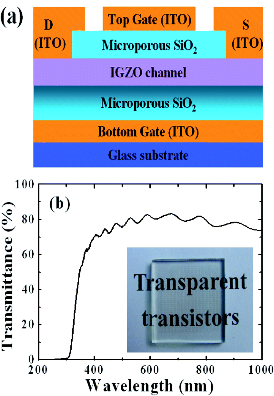 | ||
| Fig. 1 (a) Structure of the dual-gate TFT with the driving bottom gate and the control top-gate. (b) Optical transmission spectra of such TFT arrays on glass substrates. Inset: an optical image of the TFT arrays placed on background text. | ||
As shown in Fig. 2a, like other microporous-SiO2 in the previous work reported by our groups,11 these TG and BG dielectrics of such DG TFTs also show huge specific capacitance of ∼4 μF cm−2 at 20 Hz, which leads to a low operating voltage of 1.0 V. Fig. 2b shows the leakage current of the STD and DG TFTs. The leakage current of STD TFTs was ∼1 nA, however, the leakage current of DG TFTs was less than 0.2 nA, which was much smaller than that of solid polymer electrolytes or ionic liquids.12,13 Despite the nanopores existed in double gate dielectrics, the leakage current is five orders of magnitude smaller than the channel current, which guarantees the device performance will not be affected by the leakage current.
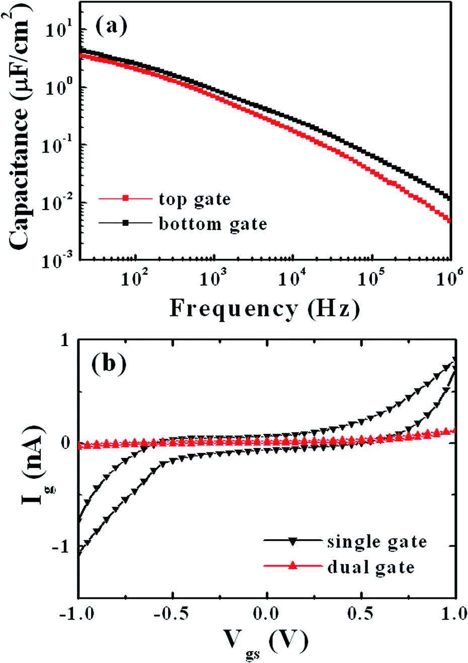 | ||
| Fig. 2 (a) Specific gate capacitance of the TG and BG dielectrics of such DG TFTs. (b) Leakage current of the STD and DG TFTs. | ||
The initial electric characteristics of such device are estimated as the conventional BG TFTs. The electron field-effect mobility (μsat) in the saturation regime is calculated using the relationship Ids = (WCbg/2L)μsat(Vbg − Vth)2, where L = 80 μm and W = 1000 μm are the channel length and width, respectively. The field-effect mobility is calculated to be ∼2.6 cm2 V−1 s−1 at Vds = 1.0 V, Vbg = 1.0 V. The corresponding carrier density of the IGZO channel layer is estimated to be 3.5 × 1013 cm−2 by N = Cbg (Vc − Von)/e. Cbg = 4.0 μF cm−2 is the bottom gate specific capacitance at 20 Hz. The Vc = 1.0 V is the bottom gate voltage bias for mobility estimation. Von = −0.4 V is the turn-on voltage of the device without a top gate bias. Fig. 3a shows the transfer characteristics of the DG TFTs in the saturation regime (Vds = 1.0 V) with top gate voltage biases in the range from 2.0 V to −2.0 V. All transfer curves were sweeping from negative to positive with a negative bias stress time of 10 s and a sweep rate of 50 mV s−1. The hysteresis window is less than 0.05 V upon sweeping forward and backward without obvious bias stress effect. Thus, we only plotted the result of forward sweeps. When Vtg is swept from 2.0 V to −2.0 V, the transfer curves systematically shift from left to right. Fig. 3b shows the (Ids)1/2–Vbg transfer curves with different Vtg. The threshold voltage (Vth), indicated by the intercepts lines with the Vbg axis, moves from a negative value of −0.13 V to a positive value of 0.5 V. These results indicate that an effectively electrostatic coupling is realized between the top gate and the IGZO channel. By the way, subthreshold swing of ∼76 mV per decade and current on/off ratio of ∼2.1 × 10⁶ are almost constant at various voltage biases of top gate.
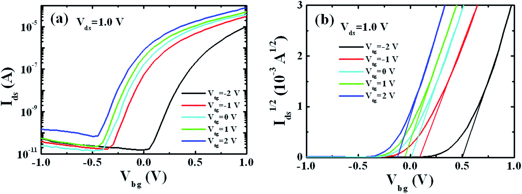 | ||
| Fig. 3 (a) The transfer characteristics of the dual-gate TFTs at different top-gate voltage biases. (b) (Ids)1/2–Vbg curves of the same device. | ||
Fig. 4a and b show the output characteristics of transparent dual-gate TFTs with different voltage bias of top gate. Linear behaviours of Ids at low Vds are observed, indicating that good ohmic contact between the IGZO channel layer and ITO source/drain electrodes were realized. When Vtg was changed from 2.0 V to −2.0 V, depletion-mode was gradually changed to enhancement-mode. So dual-gate configuration provides more flexibility in device operation.
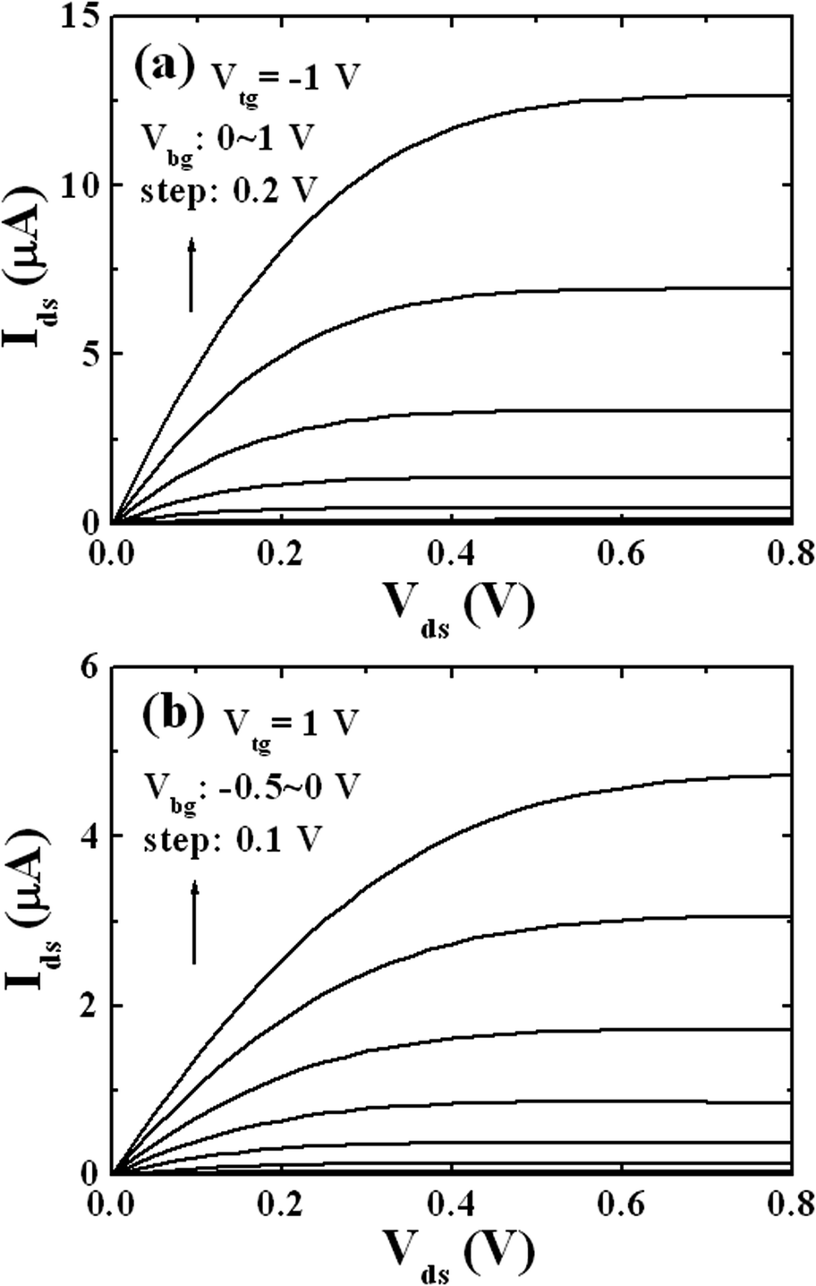 | ||
| Fig. 4 Output characteristic of the dual-gate TFTs operated at enhancement mode (a) when Vtg = −1.0 V, at depletion mode (b) when Vtg = 1.0 V. | ||
The extracted Vth and subthreshold swing (S) are presented in Fig. 5a as a function of the Vtg for DG TFTs. The asymmetric behaviour of Vth shift is due to the changeable Cbg-dielectric and Ctg-dielectric at different (positive and negative) Vtg. When Vtg ≥ 0 V, all ITO electrodes are highly conducting, and the capacitance values of Cbg-dielectric (Cbd) and Ctg-dielectric (Ctd) are equivalent to the EDL capacitance of SiO2-based electrolyte. When Vtg < 0 V, Cbd and Ctd will become smaller due to the IGZO film depletion effect induced by the negative Vtg. According to the equation: ΔVth = ΔVtgCtd/[Ctd + (Cbd + Ctd)], a larger Vth shift can be obtained when Vtg < 0 V. These results indicates that the Vth is very sensitive to the changes in the surface potential of the top gate dielectric region,14 so such DG TFTs are very promising for ion-sensitive field-effect transistors sensor applications. Simultaneously, the S has a weak dependence on the top gate bias, which indicates the value of S was almost unaffected by the Vtg. Such DG TFTs were continuously switched between the ON- and OFF-states in dynamic stress tests (periodic square-wave pulses of Vbg = −0.5 to −1.0 V, Vtg = 0 V, and Vds = 1.0 V), as shown in Fig. 5b. A drain-current on/off ratio of larger than 105 was maintained, and no obvious drain current decrease was observed. This result suggests very good switching stability of the DG TFTs with a top gate.
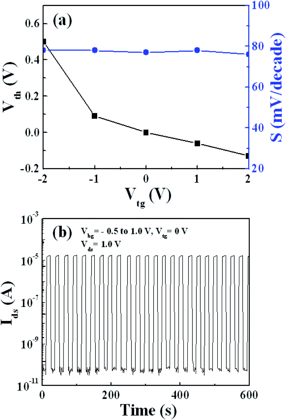 | ||
| Fig. 5 (a) The threshold voltage and subthreshold swing of the dual gate TFTs at different Vtg. (b) The switching stability driven by square-wave pulses with a period of 1 Hz. | ||
Conclusions
In conclusion, dual-gate low-voltage transparent EDL TFTs gated by PECVD-deposited microporous-SiO2 were fabricated with a top gate. Carrier density of the channel, Vth and operation mode of the devices can be tuned by the top gate. The Vth of such device can be systematically tuned from −0.13 V to 0.5 V by using a top-gate bias ranging from 2.0 V to −2.0 V. The combination of the controllability of Vth, room temperature process, low-voltage operation of the transparent dual-gate TFTs are very promising for ion-sensitive field-effect transistors sensor applications.Author contributions
Thin-film transistor and device performance was fabricated and characterized by W. D. The manuscript was prepared by W. D. and Y. T. W. D. examined and commented on the manuscript. The project was guided by W. D.Conflicts of interest
There are no conflicts to declare.Acknowledgements
This project was supported by Doctoral Science Foundation of Hunan Normal University (0531120).Notes and references
- M. Chun, J. G. Um, M. S. Park, M. D. H. Choudhury and J. Jang, AIP Adv., 2016, 6, 075217 CrossRef.
- J. C. Dutta, H. R. Thakur and G. Keshiwani, IEEE Sens. J., 2019, 19, 5692–5699 CAS.
- Y. Kamada, S. Fujita, M. Kimura, T. Hiramatsu, T. Matsuda, M. Furuta and T. Hirao, IEEE Electron Device Lett., 2011, 32, 509 CAS.
- J. Jiang, J. Sun, L. Zhu, G. Wu and Q. Wan, Appl. Phys. Lett., 2011, 99, 113504 CrossRef.
- J. Sun, J. Jiang, W. Dou and Q. Wan, IEEE Electron Device Lett., 2011, 32, 1710 CAS.
- W. Dou and Y. Tan, ACS Omega, 2019, 4, 21417 CrossRef CAS PubMed.
- W. Dou, L. Zhu, J. Jiang and Q. Wan, Appl. Phys. Lett., 2013, 102, 093509 CrossRef.
- D. Kasprowicz, IEEE Trans. Comput. Aided Des. Integrated Circ. Syst., 2019, 7, 10389–10393 Search PubMed.
- K. Tamersit, J. Comput. Electron., 2019, 18, 846–855 CrossRef CAS.
- J. M. Lee, I. T. Cho, J. H. Lee and H. I. Kwon, Jpn. J. Appl. Phys., 2009, 48, 100202 CrossRef.
- W. Dou and Y. Tan, RSC Adv., 2019, 9, 30715 RSC.
- J. H. Cho, J. Lee, Y. Xia, B. Kim, Y. Y. He, M. J. Renn, T. P. Lodge and C. D. Frisbie, Nat. Mater., 2008, 7, 900 CrossRef CAS PubMed.
- L. Zhao, K. Chen, F. Yang, M. L. Zheng, J. M. Guo, G. Q. Gu, B. Zhang, H. F. Qin, G. Cheng and Z. L. Du, Nano Energy, 2019, 62, 38–45 CrossRef CAS.
- M. J. Spijkman, J. J. Brondijk, T. T. Geuns, E. P. Smits, T. Cramer, F. Zerbetto, P. Stoliar, F. Biscarini, P. M. Blom and D. M. Leeuw, Adv. Funct. Mater., 2010, 20, 898 CrossRef CAS.
| This journal is © The Royal Society of Chemistry 2020 |