
 Open Access Article
 This Open Access Article is licensed under a Creative Commons Attribution-Non Commercial 3.0 Unported Licence
Analysis of plasma-grown carbon oxide and reduced-carbon-oxide nanowalls
Hyeokjoo Choi a,
Seok Hun Kwona,
Hyunil Kanga,
Jung Hyun Kimb and
Wonseok Choi*a
a,
Seok Hun Kwona,
Hyunil Kanga,
Jung Hyun Kimb and
Wonseok Choi*a
aDepartment of Electrical Engineering, Hanbat National University, Daejeon 34158, Republic of Korea. E-mail: wschoi@hanbat.ac.kr
bDepartment of Advanced Materials Engineering, Hanbat National University, Daejeon 34158, Republic of Korea
First published on 6th March 2020
Abstract
In this study, several characteristics of carbon oxide nanowalls (CONWs) and reduced-carbon-oxide nanowalls (rCONWs) activated using plasma and thermochemistry were investigated. To become modified CONW and rCONW, catalyst-free carbon nanowalls (CNWs) were grown on a silicon (Si) wafer via microwave-plasma-enhanced chemical vapor deposition (MPECVD) with a mixture of hydrogen (H2) and methane (CH4) gases. The CONW was modified by oxidizing a CNW on a Si wafer with plasma treatment using oxygen (O2) plasma. Afterwards, the CONW was placed in a rapid-thermal-annealing (RTA) chamber, and H2 gas was injected thereto; therefore, the CONW was reduced by H2 gas. The surface properties of the CONW and rCONW were confirmed via scanning electron microscopy (SEM). Raman spectroscopy was used for structural analysis, and the surface energy of each surface was analyzed by operating the contact angle. The chemical characteristics were observed via X-ray photoelectron spectroscopy (XPS). Hall measurements were applied to investigate the electrical characteristics.
1 Introduction
Carbon has attracted attention for a long time, and many studies for its application have been conducted.1–3 Graphite-related materials like fullerene, graphene, and carbon nanotube can be divided into classes based on their growth dimensions. Fullerene can be distinguished as a 0-dimensional carbon nanomaterial, carbon nanotube as a one-dimensional carbon nanomaterial, and graphene as a two-dimensional carbon nanomaterial. The material similar to these, carbon nanowall (CNW), is also a two-dimensional graphite nanostructure that is wall-shaped, like a vertically aligned graphene.4 Naturally, the advantages of this vertically standing carbon nanostructure are a large reaction area and remarkable electrical conductivity. Among these, the unrivaled merit of CNWs is that they are catalyst-free, unlike other carbon nanomaterials, which require a catalyst for the fabrication of graphene5 and carbon nanotubes.6 CNWs can be grown on diverse substrates through various chemical vapor deposition (CVD) methods,7–9 and can even be grown via sputtering.10CNWs with a wide reaction area can be used in many applications. Having a large reaction area, however, does not mean having high surface energy. In addition, even if the surface energy is high, if the electrical characteristics are low after the reaction, applications like gas sensors and biosensors11 will not be able to easily determine the accurate value due to their low sensitivity. Therefore, surface-activated CNWs, which have a large response area, high surface energy, and good electrical properties, will be used in more applications.
In this study, to increase the surface energy of CNWs, carbon oxide nanowalls (CONWs) were activated through oxidization, and were modified to produce reduced-carbon-oxide nanowalls (rCONWs). Microwave-plasma-enhanced chemical vapor deposition (MPECVD) is a method in which a gas composed of a desired material in the reactor is decomposed through high plasma energy, and the layers are stacked on the substrate. In addition, as high plasma energy is used, it can be synthesized through low-temperature. CNWs consisting of pure carbon were grown at 1300 W microwave power as the main source of plasma energy, and at 700 °C for 10 minutes via MPECVD with a mixture of methane (CH4) and hydrogen (H2) gases. CONWs were obtained using oxygen (O2) plasma. After that, thermochemistry was performed with H2 gas to obtain rCONWs. For the samples thus obtained, field emission scanning electron microscopy (FESEM), contact angle measurement, and Raman spectroscopy were used to determine the surface and structural properties. The chemical properties were determined via X-ray photoelectron spectroscopy (XPS), and the electrical properties were analyzed via Hall measurement.
2 Experiment
2.1 Growth of carbon nanowalls
The prepared 2 × 2 cm2 p-type silicon (Si) wafers (100) were ultrasonically cleaned with trichlorethylene (TCE), acetone, methanol, and deionized (DI) water (in that order) for cleaning the surface.12 The cleaned substrates were then dried using nitrogen (N2) gas, and were placed directly inside an MPECVD (ASTeX-type MPECVD, Woosin CryoVac, 2.45 GHz microwave) chamber. The base vacuum inside the chamber was set to 10−4 torr or less, and a mixture of H2 (25 sccm) and CH4 (55 sccm) gases was added thereto. At this time, the substrate temperature was 700 °C, the microwave power was 1300 W, and the working vacuum was 5 to 6 × 10⁻² torr. The microwaves passed from the quartz in parallel with the holder, forming a plasma ball on the substrate, through which the carbon atoms of CH4 were nucleated, and a buffer layer was formed on the substrate, and then a CNW was grown. After growing for 10 minutes, the mixture was slowly cooled to room temperature in a 1 × 10⁻² torr working vacuum.2.2 Surface activation of carbon nanowalls
The starting material, CNW, was put inside a plasma treatment equipment, and 20 sccm O2 was added to form plasma. 200 W radio frequency (RF) power was used for plasma formation, and the temperature inside the plasma treatment equipment was kept at room temperature for a minute. The working vacuum at this time was 5 × 10⁻² torr. CNW is a two-dimensional graphite nanomaterial in which graphene is formed in the shape of a wall. If too much of it is formed during the oxidation or reduction process, it is etched and blown away, and much gas collision occurs due to the wall structure. Therefore, it is important to set the appropriate time, power, and temperature for surface activation. CONW, surface-modified with a plasma treatment equipment, was placed in a rapid-thermal-annealing (RTA) chamber and was kept at 500 °C. At this time, the working vacuum was 0.1 torr, and 15 sccm H2 gas was injected for 10 minutes. The completed rCONW was kept in the chamber at 0.01 torr working vacuum, and was slowly cooled until room temperature.2.3 Analysis of the CNW, CONW, and rCONW
To confirm the surface characteristics via FESEM (Hitachi, S-4800), 5–10 kV acceleration voltages were applied at 5–15 mm distances. The surface energy was determined by the contact angle (SEO, inspection of Phoenix MT), and the average value was obtained by dropping 3 μL DI water for a total of 4 times at room temperature. Raman spectroscopy (NOST, FEX; excitation power: ∼0.3) was performed to examine the structural characteristics of the samples. In addition, the inherent peaks of all the samples were calculated, and the ID/IG and I2D/IG ratios were obtained from the Raman spectrum. The chemical components and bonds of the samples were observed through XPS (ThermoFisher Scientific, K-Alpha+) to determine the chemical properties. The electrical characteristics were confirmed via Hall measurements (ECOPIA, HMS-3000) using 1 mA current.3 Results and discussion
3.1 Surface and structural characteristics
Fig. 1 shows the contact angle13 and FESEM surface images representing the surface characteristics of the samples. The nanowalls were about 1 μm, 900 nm, and 850 nm in height, respectively. As can be seen in Fig. 1(a), the edge of the CNW was rounded. Those in Fig. 1(b) and (c), unlike CNW, appear like sharp needles. Also, the surfaces of the CONW and rCONW were uneven and rugged compared to that of the CNW. The surface of the CNW was sharply changed as the nanowalls were oxidized, and the height was lowered by a slight etching and broken bonding. At the time of reduction, the unstable functional group and H2 gas were combined to lower the heights of the nanowalls. It was also determined that the walls of the CNW, whose edges were connected to one another, were opened or set apart by oxidation.14 Fig. 1(d) shows that the CNW was hydrophobic before the oxidation of the nanowalls. As can be seen in Fig. 1(e), however, the oxidized nanowall of the CONW became hydrophilic. Fig. 1(f) shows that the contact angle of the rCONW was hydrophilic because a few functional groups remained on the surface of the nanowall, which also had increased surface energy.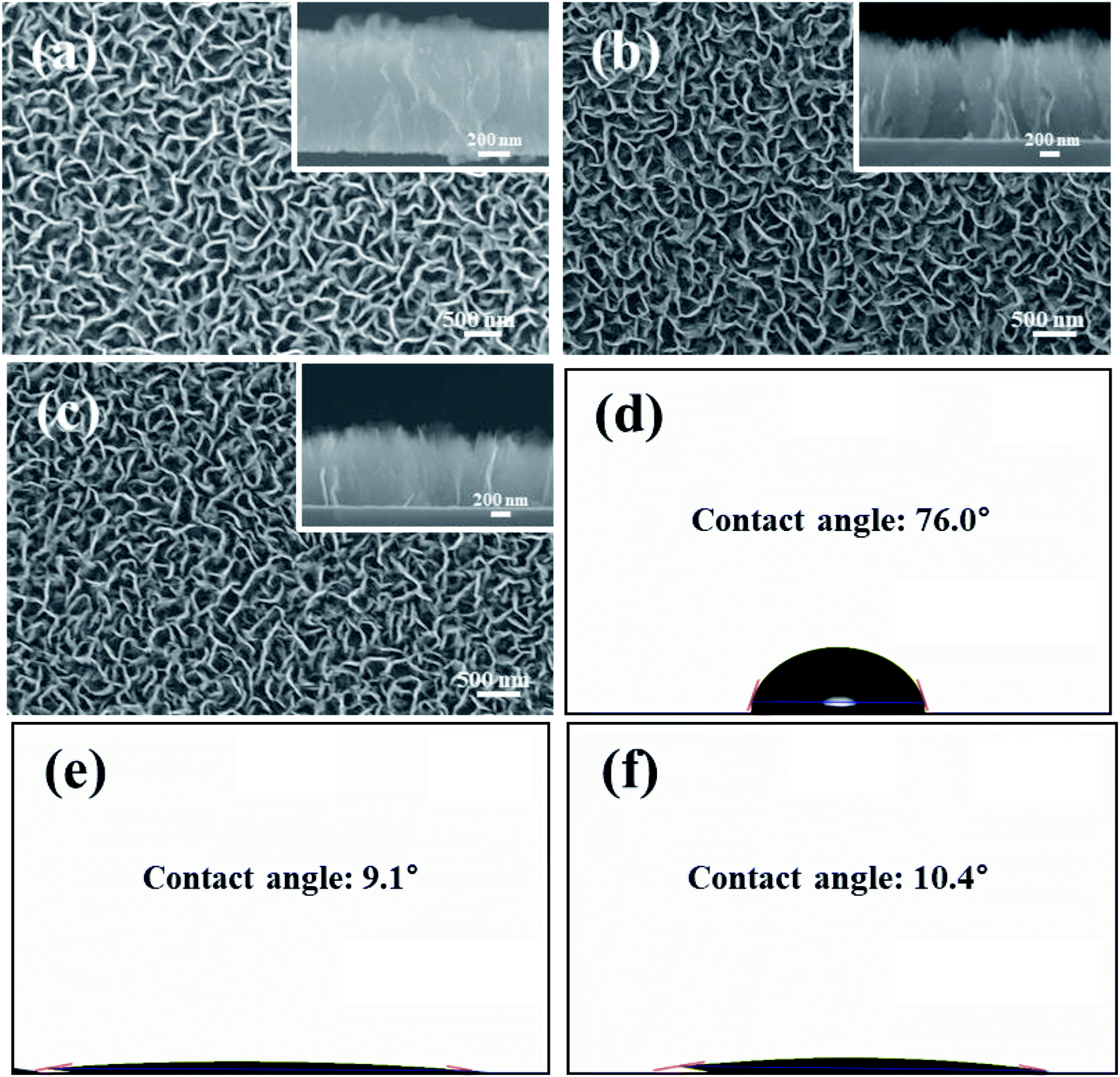 | ||
| Fig. 1 FESEM surface (left) and cross-sectional (right) images of the (a) CNW, (b) CONW, and (c) rCONW. Contact angles of the (d) CNW, (e) CONW, and (f) rCONW. | ||
Fig. 2 shows why the contact angles of the CONW and rCONW were hydrophilic. In the case of the CNW (Fig. 2(a)), when the pressure was seen acting on DI water, Pi (intrinsic pressure) due to gravity was applied. In addition, PL (Laplace pressure) was generated by the energy difference between ESW (surface energy of the nanowall) and ESB (surface energy of the buffer layer). As ESB was higher than the ESW of the CNW, PL acted in the direction opposite Pi, and the CNW had hydrophobicity. From the perspective of the CONW and rCONW, as shown in Fig. 2(b), the samples that were wall-shaped were oxidized more than the buffer layer caused by several collisions with O plasma, thereby increasing the ESW. Therefore, ESW became larger than ESB, and PL acted in the same direction as Pi, making it hydrophilic. In addition, the O atoms of the functional groups and the H atoms of the water molecules had more surface energy from the hydrogen bonding.
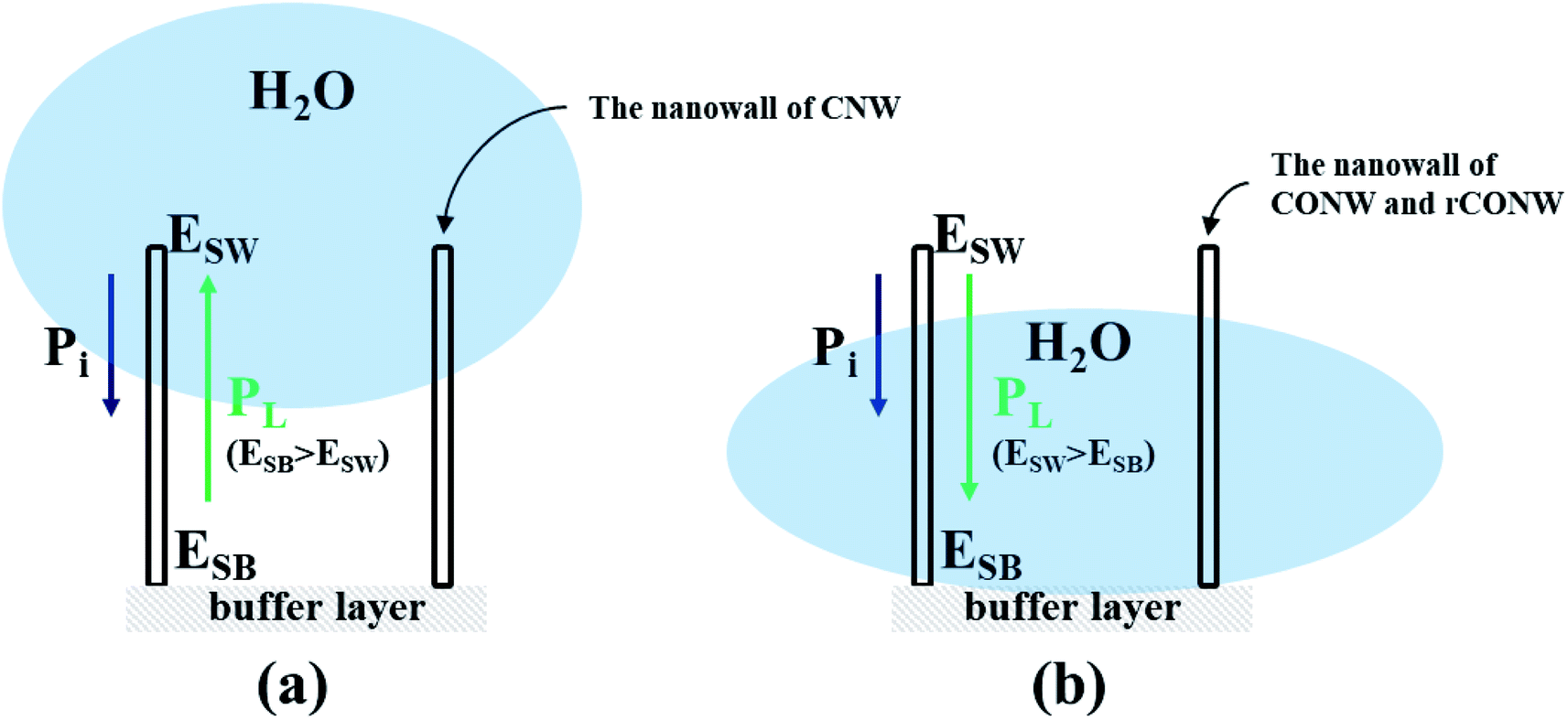 | ||
| Fig. 2 Schematic of variation in contact angle according to the energy difference between the nanowalls and the surfaces in the (a) CNW and the (b) CONW and rCONW. | ||
The structural characteristics of the samples were confirmed by the Raman spectrum. In Fig. 3(a), the D and D′ peaks showed the edges and defects of graphene, and the G peaks showed the sp2 structure. The 2D peak is a peak by π–π*, and the higher it is (which means a thin graphene layer), the lower the G peak.15,16 The D peak of the samples was shown at 1343–1345 cm−1, the G peak at 1575–1577 cm−1, and the 2D peak at 2688–2694 cm−1. Fig. 3(b) shows the ID/IG ratios expressing the defect levels of the samples, and the I2D/IG ratios representing the numbers of graphene layers. The ID/IG ratio of the CNW was the highest among the samples, and that of the rCONW was the lowest. If the measured CNW had a larger surface defect, a hydrophilic contact angle should have appeared. The contact angle, however, was hydrophobic, and the ID/IG ratio was high. This may be true for the several thin graphene layers, the branches of the CNW, because the branches grew sideways on the wall, the edges of the graphene layers, and the D and D′ peaks increased (Fig. 4). When oxidized, the branches disappeared, and the D and D′ peaks were diminished. In addition, the functional group was attached to the missing branch. As the rCONW was changed from the CONW, the functional group disappeared, the unoccupied part reverted back to the sp2 structure, and the ID/IG ratio was reduced. Similarly, the I2D/IG ratio was increased by the 2D peak of the CNW due to the thin branches compared to the nanowall and buffer layer, but the 2D peaks of the CONW and rCONW appeared to have decreased due to the branches that had disappeared.
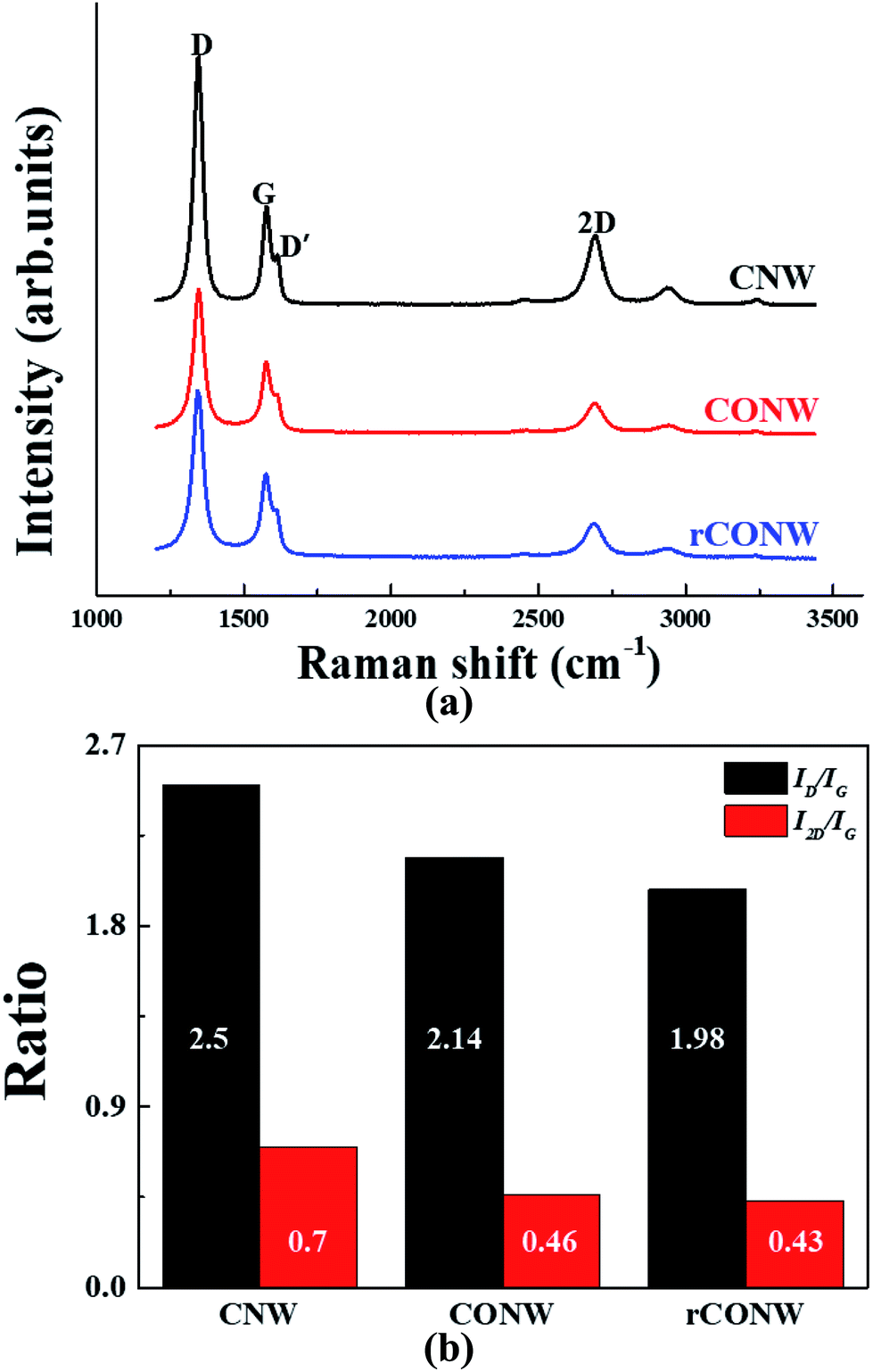 | ||
| Fig. 3 (a) Raman spectrum of the samples. (b) ID/IG and I2D/IG ratios of the samples. | ||
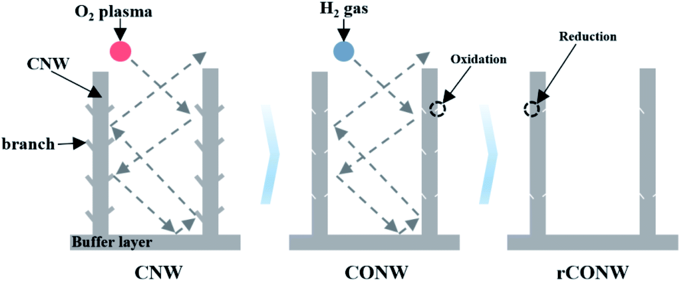 | ||
| Fig. 4 Structural schematic of variation in the samples by multiple activation collision. | ||
3.2 Chemical characteristics
XPS receives up to ∼10 nm photoelectrons emitted from the surface due to the photoelectric effect of X-ray. Fig. 5(a) shows the CNW's XPS survey results, which show faint O1s peaks on the nanowalls arising from the air exposure during the experiment. In Fig. 5(b), C1s, O1s, and O auger peaks can be seen in the XPS survey results of the CONW. Compared with Fig. 5(a), a C1s peak similar to a large O1s peak can be seen, indicating that the CONW was well formed. Fig. 5(c) shows the XPS survey results of the rCONW, displaying a larger O1s peak than the CNW in Fig. 5(a), and a smaller O1s peak than the CONW in Fig. 5(b). Fig. 5(b) and (c) also show the O auger peak caused by the diverse bonds of the O atoms on the surface.17 Therefore, the functional group attached to the nanowall and the buffer layer.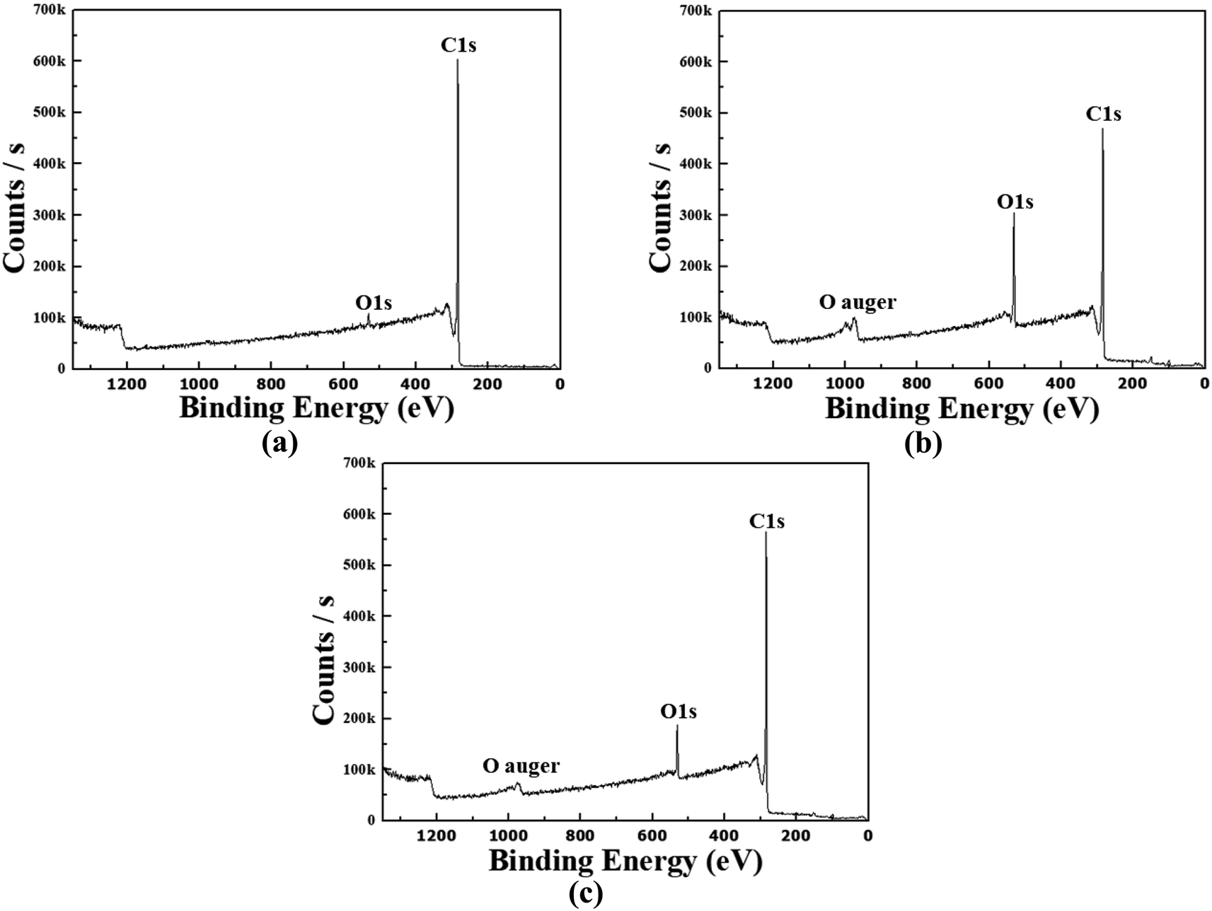 | ||
| Fig. 5 XPS survey results of the (a) CNW, (b) CONW, and (c) rCONW. | ||
Fig. 6(a) shows the C1s peak of the CNW. There are sp3, sp2, and π bonds owing to the CNW mechanism.14,18,19 In Fig. 6(b), which shows the C1s peak of the CONW, the C–O and C![[double bond, length as m-dash]](https://www.rsc.org/images/entities/char_e001.gif) O bonds (the functional group) can be seen as having increased compared to those in Fig. 6(a). It can also be seen that the sp3 bond increased compared to the sp2 bond. In other words, O2 plasma breaks the sp2 bond of CNW and strengthens the bond between the C and O atoms. Fig. 6(c) shows the C1s peak of the rCONW. The ratio of sp2 and sp3 bonds in the CNW, which had more sufficient sp2 than sp3 bonds, was similar, but C–O and CO bonds are shown. In addition, the sp2 bond grew, and the functional group was reduced compared to the CONW. Therefore, the rCONW was reduced due to the combination of H2 and functional groups that attached to the carbon at high temperatures. In addition, owing to the remaining binding energy resulting from the reduction, it is expected that the sp2 bond will further increase due to the bond with carbon.
O bonds (the functional group) can be seen as having increased compared to those in Fig. 6(a). It can also be seen that the sp3 bond increased compared to the sp2 bond. In other words, O2 plasma breaks the sp2 bond of CNW and strengthens the bond between the C and O atoms. Fig. 6(c) shows the C1s peak of the rCONW. The ratio of sp2 and sp3 bonds in the CNW, which had more sufficient sp2 than sp3 bonds, was similar, but C–O and CO bonds are shown. In addition, the sp2 bond grew, and the functional group was reduced compared to the CONW. Therefore, the rCONW was reduced due to the combination of H2 and functional groups that attached to the carbon at high temperatures. In addition, owing to the remaining binding energy resulting from the reduction, it is expected that the sp2 bond will further increase due to the bond with carbon.
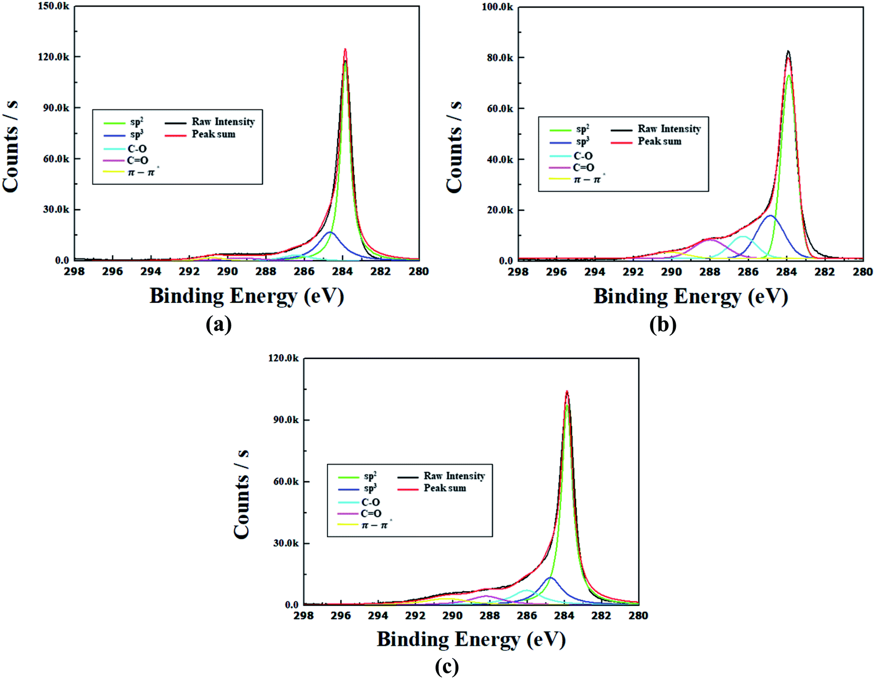 | ||
| Fig. 6 XPS C1s peaks of the (a) CNW, (b) CONW, and (c) rCONW. | ||
3.3 Electrical characteristics
Fig. 7 shows the average value obtained from the Hall measurements in the five experiments. The electrical characteristics of the CONW decreased due to the surface activation of the CNW, resulting in more functional groups and fewer sp2 bonds. On the other hand, the rCONW's electrical characteristics improved when the functional group of the CONW was reduced and the sp2 bond was increased. The rCONW, however, had a smaller C1s peak and a larger O1s peak than the CNW for achieving the electrical characteristics of the CNW. In other words, the electrical properties were lower than those of the CNW due to the oxidation of the nanowalls and the buffer layer.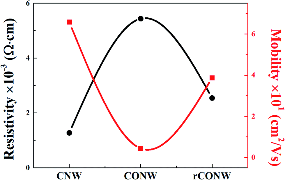 | ||
| Fig. 7 Electrical characteristic of the CNW, CONW, and rCONW determined via Hall measurement. | ||
4 Conclusion
In this study, carbon oxide nanowalls (CONWs) and reduced-carbon-oxide nanowalls (rCONWs) were created to improve the surface energy and achieve the electrical characteristics of carbon nanowalls (CNWs). A CNW sample was grown on a silicon (Si) wafer using microwave-plasma-enhanced chemical vapor deposition (MPECVD), and was oxidized in a plasma washer to activate it. The CONW (the activated CNW) was reduced by hydrogen (H2) gas to modified rCONW via rapid thermal annealing (RTA) and the thermochemical method. Field emission scanning electron microscopy (FESEM), contact angle measurement, and Raman spectroscopy were used to confirm the surface and structural characteristics. Through the contact angle measurement, the surface energy of the CONW was found to be higher than that of the CNW. The contact angle of the rCONW was slightly higher than that of the CONW, but it was much lower than that of the CNW. It appears that the contact angle variation was due to the difference in surface energy between the nanowall and the buffer layer. With regard to the structural characteristics, the ID/IG and I2D/IG ratios were the highest in the CNW, and the ratios of the CONW and rCONW were expected to be changed by the branches of the CNW. The chemical properties of the samples were examined via X-ray photoelectron spectroscopy (XPS) analysis, and it was found that the sp2 bonding peak at the C1s peak of the CONW was smaller than that of the CNW, promoting bonding between the O atoms and the surface of the nanowall, and that the functional group was attached thereto. In the case of the rCONW, the sp2 bonding peak became similar to the CNW's, and it was confirmed that the functional group was still attached. The electrical characteristics were observed through Hall measurement, and it was found that those of the CNW with graphene properties were the highest among all the samples, and that those of the CONW that had been deprived of sp2 bonding were the lowest. In the rCONW example, the electrical characteristics improved compared to the CONW when the sp2 bonding was increased, as determined via XPS analysis. rCONW, which has higher surface energy than and similar electrical characteristics as CNW, is expected to be used as a material for sensors or other applications.Conflicts of interest
There are no conflicts to declare.Acknowledgements
This work was supported by Korea Institute of Energy Technology Evaluation and Planning (KETEP) and the Ministry of Trade, Industry, & Energy (MOTIE) of the Republic of Korea (No. 20184030201900), and also by a Korea Science and Engineering Foundation (KOSEF) grant funded by the South Korean government (MEST) (No. NRF-2018R1D1A1B07046804).References
- S. Yang, Y. Cheng, X. Xiao and H. Pang, Development and application of carbon fiber in batteries, Chem. Eng. J., 2019, 123294, DOI:10.1016/j.cej.2019.123294.
- Z. Li, L. Wang, L. Yu, Y. Feng and W. Feng, Carbon-based functional nanomaterials: preparation, properties and applications, Compos. Sci. Technol., 2019, 179, 10–40, DOI:10.1016/j.compscitech.2019.04.028.
- A. Fiorani, J. P. Merino, A. Zanut, A. Criado, G. Valenti, M. Prato and F. Paolucci, Advanced carbon nanomaterials for electrochemiluminescent biosensor applications, Curr. Opin. Electrochem., 2019, 16, 66–74, DOI:10.1016/j.coelec.2019.04.018.
- M. Hiramatsu and M. Hori, Carbon Nanowalls: Synthesis and Emerging Applications, Springer, New York, 2010 Search PubMed.
- L. Han, J. J. Liu, Z. Zhao, S. Chen, Z. Ma and L. Zhao, Two-step method preparation of graphene without hydrogen on methanol pretreatment copper substrate by PECVD at low temperature, Phys. E, 2016, 84, 249–257, DOI:10.1016/j.physe.2016.04.013.
- V. C. S. Tony, C. H. Voon, B. Y. Lim, Y. Al-Douri, S. C. B. Gopinath, M. K. MdArshad, S. T. Ten, N. A. Parmin and A. R. Ruslinda, Synthesis of silicon carbide nanomaterials by microwave heating: effect of types of carbon nanotubes, Solid State Sci., 2019, 98, 106023, DOI:10.1016/j.solidstatesciences.2019.106023.
- D. G. Batryshev, Y. Yerlanuly, T. S. Ramazanov, M. K. Dosbolayev and M. T. Gabdullin, Elaboration of carbon nanowalls using radio frequency plasma enhanced chemical vapor deposition, Mater. Today: Proc., 2018, 5(11), 22764–22769, DOI:10.1016/j.matpr.2018.07.088.
- D. Banerjee, S. Mukherjee and K. K. Chattopadhyay, Synthesis of amorphous carbon nanowalls by DC-PECVD on different substrates and study of its field emission properties, Appl. Surf. Sci., 2011, 257(8), 3717–3722, DOI:10.1016/j.apsusc.2010.11.119.
- S. Y. Kim, S. K. Shin, H. Kim, Y.-H. Jung, H. Kang, W. S. Choi and G. B. Kweon, Synthesis of Carbon Nanowalls by Microwave PECVD for Battery Electrode, Transactions on Electrical and Electronic Materials, 2015, 16, 198–200, DOI:10.4313/teem.2015.16.4.198.
- W.-C. Shih, J.-M. Jeng, C.-T. Huang and J.-T. Lo, Fabrication of carbon nanoflakes by RF sputtering for field emission applications, Vacuum, 2010, 84(12), 1452–1456, DOI:10.1016/j.vacuum.2010.01.049.
- Y. Vlamidis, I. Gualandi and D. Tonelli, Amperometric biosensors based on reduced GO and MWCNTs composite for polyphenols detection in fruit juices, J. Electroanal. Chem., 2017, 799, 285–292, DOI:10.1016/j.jelechem.2017.06.012.
- W. Kern and D. A. Puotinen, Cleaning solutions based on hydrogen peroxide for use in silicon semiconductor technology, RCA Rev., 1970, 31, 187 CAS.
- B. Han, S. Liang, Bo Wang, J. Zheng, X. Xie, K. Xiao, X. Wang and X. Huang, Simultaneous determination of surface energy and roughness of dense membranes by a modified contact angle method, Colloids Surf., A, 2019, 562, 370–376, DOI:10.1016/j.colsurfa.2018.11.059.
- B. Zheng, Y. Yang, J. Chen, K. Yu, J. Yan and K. Cen, Plasma-enhanced chemical vapor deposition synthesis of vertically oriented graphene nanosheets, Nanoscale, 2013, 5, 5180, 10.1039/c3nr33449j.
- L. A. Pérez, N. Bajales and G. I. Lacconi, Raman spectroscopy coupled with AFM scan head: a versatile combination for tailoring graphene oxide/reduced graphene oxide hybrid materials, Appl. Surf. Sci., 2019, 495, 143539, DOI:10.1016/j.apsusc.2019.143539.
- D. Graf, F. Molitor, K. Ensslin, C. Stampfer, A. Jungen and C. Hierold, et al., Spatially resolved Raman spectroscopy of single-and few-layer graphene, Nano Lett., 2007, 7(2), 238–242, DOI:10.1021/nl061702a.
- R. Al-Gaashani, A. Najjar, Y. Zakaria, S. Mansour and M. A. Atieha, XPS and structural studies of high quality graphene oxide and reduced graphene oxide prepared by different chemical oxidation methods, Ceram. Int., 2019, 45(11), 14439–14448, DOI:10.1016/j.ceramint.2019.04.165.
- L. X. Zhang, Z. Sun, J. L. Qi, J. M. Shi, T. D. Hao and J. C. Feng, Understanding the growth mechanism of vertically aligned graphene and control of its wettability, Carbon, 2016, 103, 339–345, DOI:10.1016/j.carbon.2016.03.029.
- J. Zhao, M. Shaygan, J. Eckert, M. Meyyappan and M. H. Rümmeli, A Growth Mechanism for Free-Standing Vertical Graphene, Nano Lett., 2014, 14, 3064–3071, DOI:10.1021/nl501039c.
| This journal is © The Royal Society of Chemistry 2020 |