
 Open Access Article
 This Open Access Article is licensed under a Creative Commons Attribution-Non Commercial 3.0 Unported Licence
Dielectric and electrical properties of annealed ZnS thin films. The appearance of the OLPT conduction mechanism in chalcogenides
J. Koaiba,
N. Bouguilaa,
H. Abassi *b,
N. Moutiaa,
M. Krainia,
A. Timoumicd,
C. Vázquez-Vázqueze,
K. Khirounia and
S. Alayaa
*b,
N. Moutiaa,
M. Krainia,
A. Timoumicd,
C. Vázquez-Vázqueze,
K. Khirounia and
S. Alayaa
aLaboratoire de Physique des Matériaux et des Nanomatériaux appliquée à l'environnement, Faculté des Sciences, Université de Gabès, Cité Erriadh, Zrig, 6072 Gabès, Tunisia
bLaboratoire de Caractérisations, Applications et Modélisation de Matériaux, Faculté des Sciences de Tunis, Université Tunis El Manar, Campus Universitaire, 1068, Tunis, Tunisia. E-mail: henda.abassi@gmail.com
cPhotovoltaic and Semiconductor Materials Laboratory, National Engineering School of Tunis, Belvedere PO Box 37, 1002 Tunis, Tunisia
dThin Film and Solar Cells Laboratory, Department of Physics, Faculty of Applied Science, Umm AL-Qura University, 21955 Makkah, Saudi Arabia
eLaboratory of Magnetism and Nanotechnology (NANOMAG), Department of Physical Chemistry, Faculty of Chemistry, Universidade de Santiago de Compostela, 15782 Santiago de Compostela, Spain
First published on 5th March 2020
Abstract
The annealing temperature (Ta) dependence of the structural, morphological, electrical and dielectric properties of ZnS thin films was investigated. In this work, we consider the as-deposited and annealed ZnS thin films at different temperatures. The as-deposited films were amorphous in nature. However, the films annealed at Ta ≥ 673 K, exhibited a hexagonal structure with (002) preferential orientation. The post annealing caused an improvement in crystallinity. The best one was observed at Ta = 723 K. Grain size increased from 7 nm to 25 nm as annealing temperature was increased from 673 K to 723 K. The surface of annealed samples is homogenous and uniform and the rms roughness is dependent on the annealing temperature: it increases with temperature within the range 5–50 nm. The film electrical conductance is found to be dependent on frequency measurement and annealing temperature: the dc conductance exhibits semi-conductor behavior for all ZnS films over the explored range of temperature and the conductance was found to enhance with increasing annealing temperature up to 623 K. In addition, it was observed that the highest conductance and lowest activation energy of ZnS films were obtained at an annealing temperature of 623 K. The mechanism of alternating current ac conductance can be reasonably explained in terms of the overlapping-large polaron tunnelling (OLPT) model for samples annealed at 623 K and 673 K. To our knowledge, this conduction mechanism was rarely found in chalcogenide materials. A significant change of Nyquist plot with annealing temperature was noted permitting the correlation between the microstructure and its electrical properties. The impedance analysis investigated that the relaxation process is well pronounced for the both annealed films at 623 K and 673 K. The dielectric behavior was associated to the polarization effect, an improvement on the dielectric constant ε′ and dielectric loss ε′′ with annealing was noticed.
1. Introduction
Zinc sulfide (ZnS) is a promising II-VI compound semiconductor belonging to the chalocgenide materials. They have immense technological importance in different applied branches of science and technology, because of its excellent catalytic, optoelectronic, and piezoelectric properties. It has been evinced to have diverse applications in electronic, optoelectronic, and electrochemical devices, such as photo catalysis, solar cell, infra-red window, cathode-ray tubes (CRT) and field emission displays (FED).1 Recently it is used for electroluminescent devices and photodiodes.2–4 In addition to the low cost, the availability of precursors, the ease of preparation and the chemical stability, it has a wide direct band gap of 3.72 eV and 3.77 eV for cubic and hexagonal phases, respectively. It has a high absorption coefficient in the visible range of the optical spectrum and enhanced electrical properties.5 ZnS thin films can be fabricated by molecular beam epitaxy (MBE),6 sputtering,7 metal organic vapor chemical deposition (MOCVD),8,9 different wet chemical synthesis methods10–14 and spray pyrolysis. The last technique is one of the simplest and efficient methods for fabrication of large area films and it offers an easy way to incorporate any dopant by adding it to the starting spray solution.15–17The properties of ZnS thin films are not only influenced by the deposition techniques but also by the post thermal treatment. Annealing has an important effect on the crystallinity of the thin film in terms of grain size, residual strain, and the defect density.18 Many works reported the influence of annealing temperature on the improvement of grain size of ZnS films,19 but only few works have been reported on the study of the effect of annealing temperature on electrical and dielectric properties of ZnS thin films.20–22 These works investigate that the electrical properties of zinc sulphide can be modified by different factors, among them the change of the grain size. Modification of the grain sizes influenced on the electrical and dielectric properties.
E. Al-Fawade et al.21 had studied the influence of annealing temperature on the structural and opto-electronic properties of ZnS thin films and they observed that the dc conductivity at room temperature decreases with the increase of annealing temperatures. This is because of the improved crystallinity with the increase of the grain size and to elimination of some defects. R. Jeyachitra et al.22 investigated the relation between resistivity of ZnS thin films deposited by vacuum evaporation method and its structural change. They found that the decrease of resistivity of ZnS films is related to the improvement in crystallinity of the films.
The study of dc and ac electrical conductance provides information about the behavior of the free and localized electric charge carriers which plays an important role to understand the electric and then dielectric polarization mechanism.
In this paper, we present a study of the effects of annealing temperature not only on the structural and morphological properties, but also on ac conductivity and dielectric properties of sprayed ZnS films.
2. Experimental details
ZnS films have been grown on glass slides by spray pyrolysis technique. The films were prepared from an aqueous solution containing zinc chloride (ZnCl2) and thiourea [SC(NH2)2], as sources of Zn2+ and S2− respectively with initial molar ratio Zn![[thin space (1/6-em)]](https://www.rsc.org/images/entities/char_2009.gif) :S of 1. Distilled water was used as solvent. The experimental setup involves a heating system to preserve the substrate at the desired temperature. The substrate temperature was fixed at 623 K and measured by a thermocouple placed near the substrate. The flow rates of solution and the air flow were fixed at 2 ml min−1 and 10 ml min−1, respectively. When this temperature was attained and stabilized, the solution was sprayed for 20 min. The experimental setup involves a heating system to keep the substrate at the wished temperature. At the end of the deposit, we let the substrates cooling on the plate until the ambient temperature.
:S of 1. Distilled water was used as solvent. The experimental setup involves a heating system to preserve the substrate at the desired temperature. The substrate temperature was fixed at 623 K and measured by a thermocouple placed near the substrate. The flow rates of solution and the air flow were fixed at 2 ml min−1 and 10 ml min−1, respectively. When this temperature was attained and stabilized, the solution was sprayed for 20 min. The experimental setup involves a heating system to keep the substrate at the wished temperature. At the end of the deposit, we let the substrates cooling on the plate until the ambient temperature.
It is well known that as-deposited films are very resistive. To enhance their conductivity, the samples were then sealed into Pyrex tube with a little amount of sulfur at a pressure of 10−3 torr and were then annealed at temperatures (Ta) varying from 573 K to 723 K according to profile illustrated in Fig. 1.
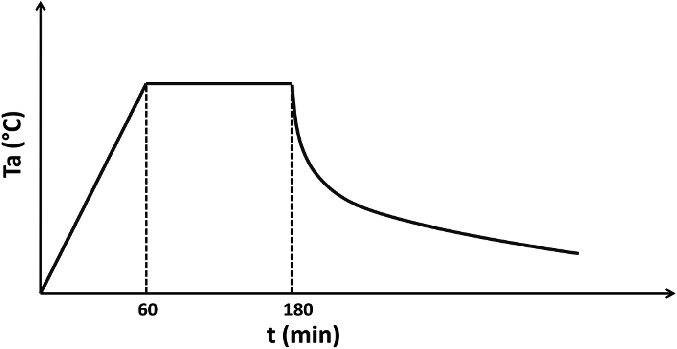 | ||
| Fig. 1 Profile of annealed temperature evolution versus time. | ||
Structural and morphological characterization of the prepared films have been carried out using X-ray diffraction (XRD) (Philips PW 1729 XRD diffractometer), atomic force microscopy AFM (Nanoscope II-Digital Instruments) and SEM images were taken with a ZEISS FE-SEM ULTRA Plus (equipped with EDX analyzer) microscope. The chemical composition and their atomic concentrations were studied with the help of energy dispersive spectroscopy (EDS). For electrical measurements, two-electrodes of silver were realized by vacuum evaporation technique. An Agilent 4294A impedance analyzer was used to collect impedance measurements over a wide frequency range (40 Hz to 100 MHz). A parallel circuit mode was used to measure both the conductance G and the capacitance C. The voltage amplitude of the alternating signal was fixed at 200 mV to get a best ratio of signal/noise. The sample was placed in liquid nitrogen cryostat to vary the temperature between 300 K and 660 K.
3. Results and discussion
3.1. Structural and morphological analysis
Structural properties of prepared samples were studied by XRD. Fig. 2 shows the XRD patterns of ZnS samples deposited by spray pyrolysis technique and annealed at different temperatures during 2 h.23 The diffractograms show clearly that the as-deposited and annealed films with temperature Ta < 673 K have an amorphous structure. While the films annealed at Ta ≥ 673 K are partially transformed into a polycrystalline structure corresponding to hexagonal wurtzite phase of ZnS, characterized by preferred orientation (002). The grain size D was determined by using the FHWM of the (002) main peak and Scherrer formula:24
 | (1) |
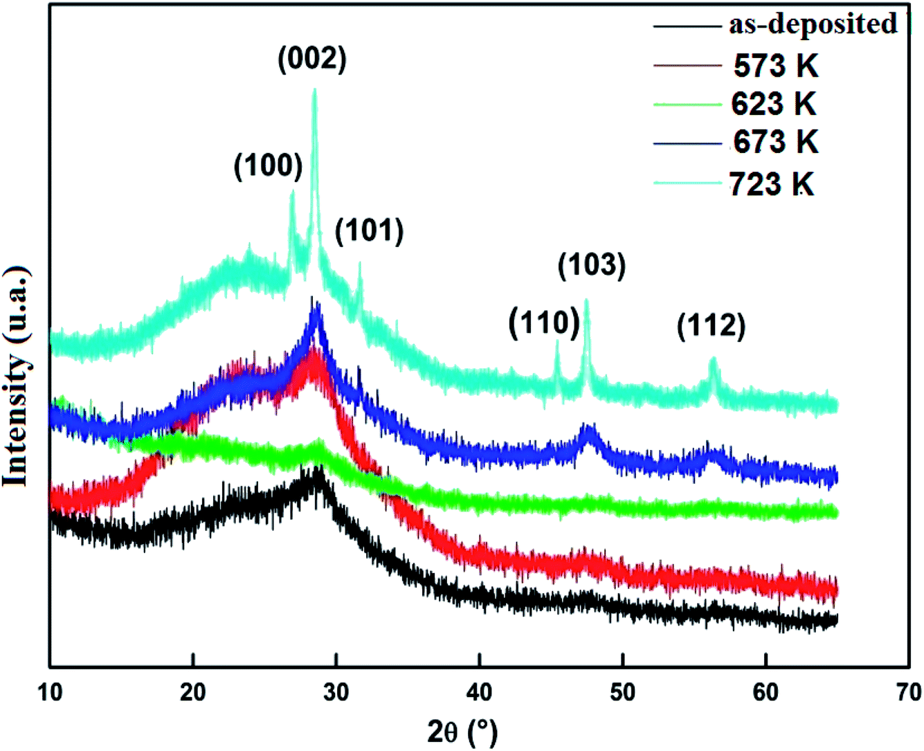 | ||
| Fig. 2 XRD patterns of as-deposited and vacuum annealed ZnS films. | ||
The film grain size is found to increase from 7 to 25 nm when the annealing temperature increases from 673 K to 723 K. This may be due to the fact that annealing would cause coalescence of dispersed grain agglomerations. At high annealing temperatures, a sufficient thermal energy is furnished, which facilitates the coalescence of the adjacent grains and results in apparent grain growth.25
The surface morphology of the layers was studied by AFM. The 2D and 3D images are displayed in Fig. 3.23 We observed from these images the continuous growth of the layers. It can be seen that by increasing the annealing temperature the grain size and the roughness change. The root mean square roughness value increases with annealing temperature and it is found to be in the range 5–50 nm. Such behavior indicates that when the annealing temperature rises, the grain becomes larger along with negligible valley spacing between the islands. Hence, the film growth proceeds through agglomeration of the islands with increasing of annealing temperature. As annealing was done under sulfur atmosphere, the increase of roughness due to sulfur exodiffusion is excluded.
 | ||
| Fig. 3 2D and 3D AFM images of ZnS films at various annealing temperatures. | ||
The SEM micrographs of wide surface morphologies of as-deposited and annealed films at different temperatures are shown in Fig. 4(a–e). SEM images reveal that the surface of the as-deposited and annealed films at 573 K and 623 K is smooth and uniform while a crack could be observed in as-deposited films and the annealed one at 623 K. For Ta ≤ 623 K, no grains are noticed indicating an amorphous phase for as-deposited and annealed films at these temperatures. These results confirmed those obtained by X-ray diffraction. For Ta > 623 K, the annealed films have good adherence on the substrates without cracks. Moreover, the films are covered by hexagonal grains, whose size increases with increasing annealing temperature. The increase of the grain size is due to the agglomeration of smaller ZnS grains.26
 | ||
| Fig. 4 SEM images of the as-deposited and annealed ZnS films at different temperatures. | ||
3.2. EDS analysis
Fig. 5 presents the typical EDS spectrum of the as-deposited and annealed ZnS films at different temperatures, which reveal that all the films contain the elements Zn and S as expected, with presence of some impurities such as Si, Ca, Na, C, O and Cl which are originated probably from the glass substrates and unreacted precursor. The atomic ratio compositions of sulfur and zinc in the films are presented in Table 1. It is obvious that the measured S/Zn ratio in all thin films is lower than the theoretical stoichiometry. Such result indicates the presence of sulphur vacancies (surplus zinc).27 The existence of the excess zinc is strongly supported by the electrical characterization of the films. | ||
| Fig. 5 A typical EDS spectrum of as-deposited ZnS films. | ||
| S (at%) | Zn (at%) | S/Zn | |
|---|---|---|---|
| As-deposited | 48.55 | 51.45 | 0.94 |
| 573 K | 44.18 | 55.82 | 0.79 |
| 623 K | 42.53 | 57.47 | 0.74 |
| 673 K | 45.77 | 54.23 | 0.84 |
| 723 K | 45.53 | 54.47 | 0.83 |
3.3. Dielectric studies
The frequency dependence of dielectric constant ε′ at different temperatures of the as-deposited and annealed ZnS films is presented in Fig. 6. For un-annealed sample, the dielectric constant decreases rapidly with increasing frequency, then increases to stabilize around 10−1 at high frequency regardless of the temperature. For each temperature, it appears frequency window in which the real part of the constant dielectric is very low or even negligible. A similar graph was theoretically predicted by different authors28,29 for polarization. It was also correlated with the ZnS band structure. This behavior in the explored frequency ranges can be explained by the existence of carrier traps in materials. Before the annealing, the material contains different typical of electron traps which begin to be emitted from a given frequency f(T). As the free charge carriers concentration increased, the dielectric constant ε′ decreases. For a particular frequency characteristic of traps, a resonance phenomenon was observed, the traps were bleed out suddenly and lower dielectric constant ε′ was obtained. Beyond the resonance frequency, traps can't follow the signal and emit the carriers. The thermal annealing is curing the material, improving the crystallinity and the dielectric constant ε′ find its classic behavior with the frequency.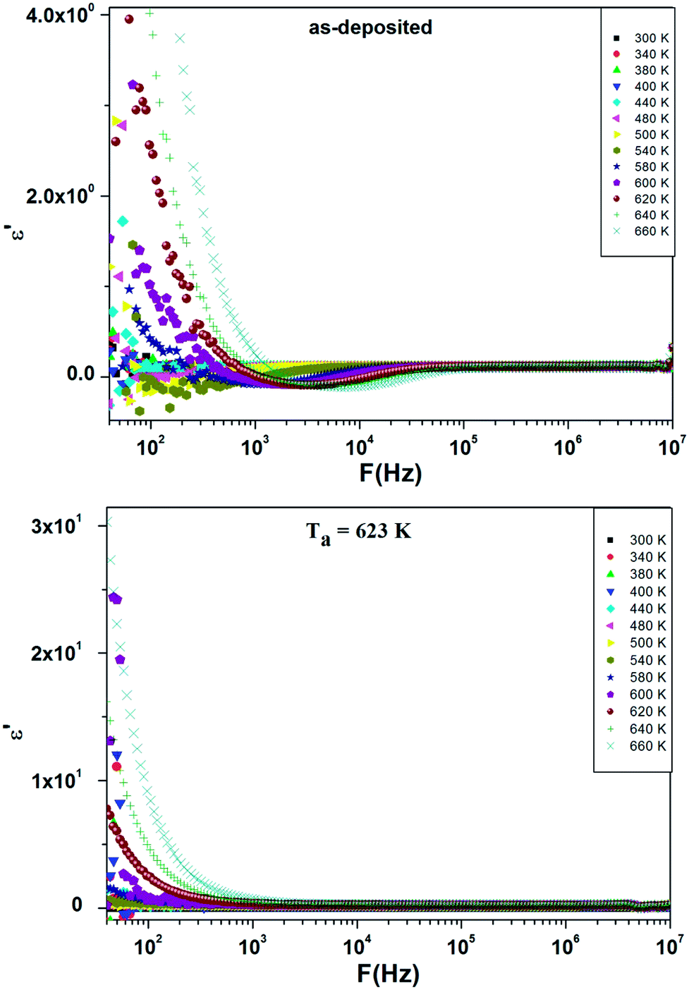 | ||
| Fig. 6 Frequency dependence of ε′ at different temperatures for as-deposited and annealed ZnS films at Ta = 623 K. | ||
Fig. 7 presents the frequency dependence of dielectric loss ε′′ at different temperatures. Depending on frequency, the dielectric loss ε′′ decreases as frequency increases. In the low frequency regions, the dielectric loss of annealed films has high values than for as-deposited films. These high values are attributed to the presence of space charge polarization created by the electrode sample contact and can be also due to the contribution of different types of polarization mechanism.30 Besides, the decrease of ε′′ with frequency is explained as follows: by increasing frequency the charge carriers become incapable to pursue the rapid excitation change; hence they lag behind the alternative excitation signal.31 In other hand, the dielectric loss ε′′ increases with increasing temperature. The mobility of charge carriers rises with temperature, increasing the polarization and resulting high values of dielectric loss. The higher values of dielectric loss at higher temperature are attributed to the accumulation of charge at grain boundaries.32 Indeed, the evolution of ε′′ is impacted by several factors33 like the lattice vibration mode, the oxygen vacancies, the presence of secondary phases34 and the grain size.35 Thus, the increment dielectric loss with temperature is a result of the impact of temperature on these intrinsic and extrinsic factors which were temperature dependent. The increase of dielectric loss with annealing temperature is due to the increase of grain size as investigated by structural analysis and to the substitution of the sulfur by oxygen in the lattice which induced by thermal annealing.
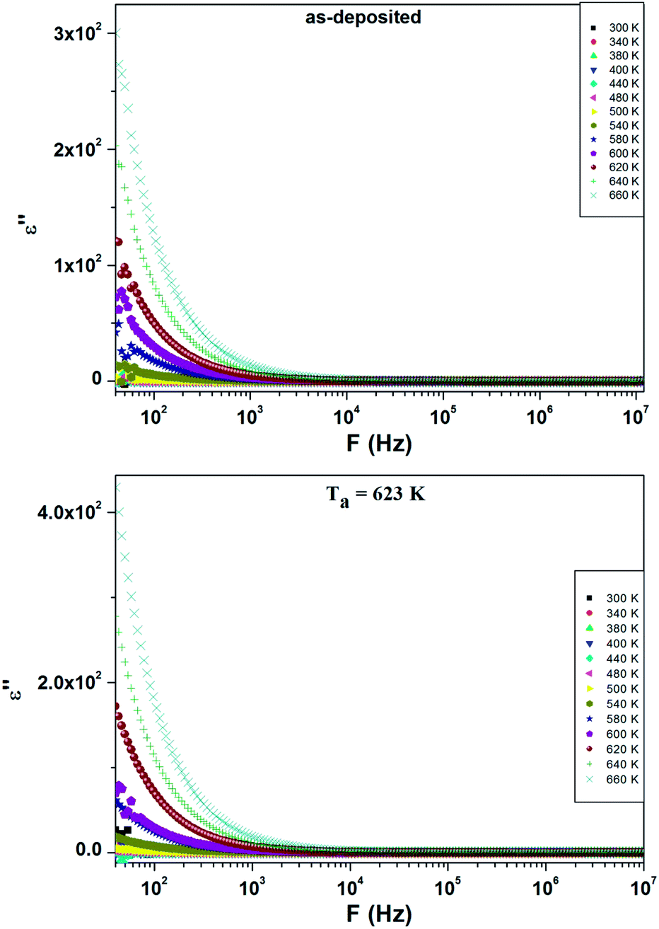 | ||
| Fig. 7 Frequency dependence of ε′′ at different temperatures for as-deposited and annealed ZnS films at Ta = 623 K. | ||
Fig. 8 shows the temperature variation of ε′′ at different frequencies. It is noticed that the dielectric loss is almost constant below 500 K and then, starts to increase steadily with increasing temperature. The increase in ε′′ can be ascribed to the thermally activated transport of space charges.36 The higher value of ε′′ at lower frequency is due to the charge accumulation at grain boundaries.37
 | ||
| Fig. 8 Temperature dependence of ε′′ at different frequencies for as-deposited and annealed ZnS films at Ta = 623 K. | ||
3.4. Electrical studies
The variation of ac conductance with frequency at 400 K for as-deposited and annealed ZnS films is reported on Fig. 9. It is obvious that the ac conductivity increases up to annealing temperature equal to 623 K and then it decreases for higher annealing temperature.
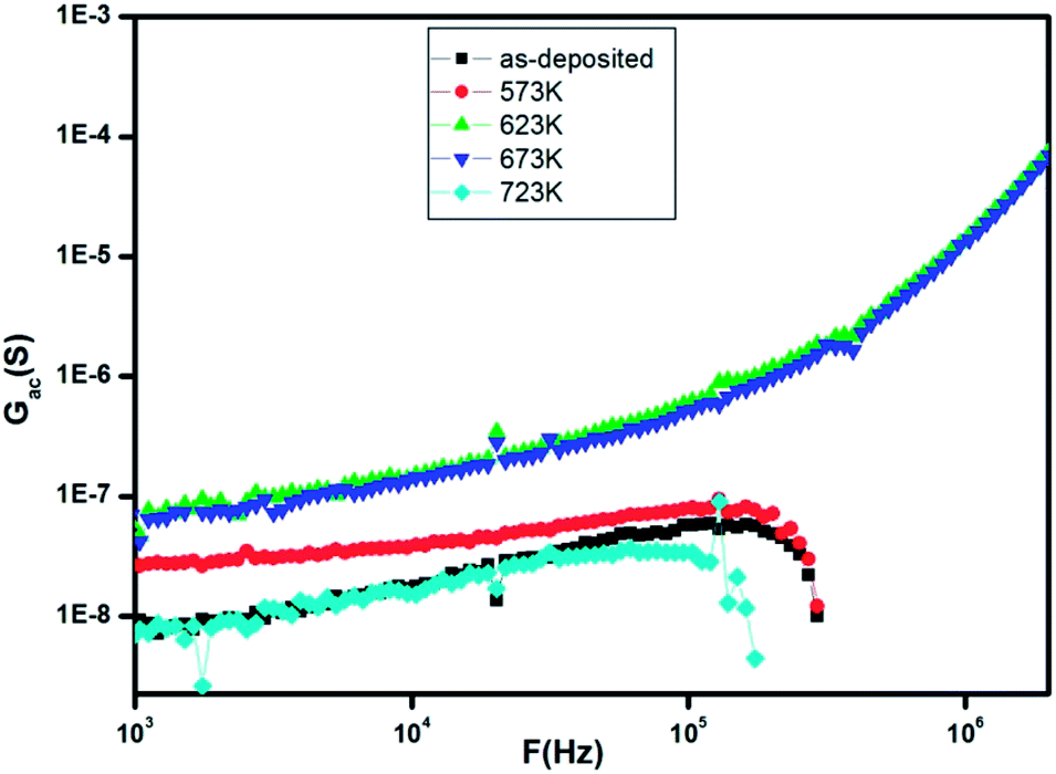 | ||
| Fig. 9 The frequency dependence of the conductance (Gac) at 400 K for as-deposited and annealed ZnS films at different temperatures. | ||
The initial increase of ac conductance with increasing annealing temperature can be interpreted by the increase of grain size which resulting a reduction in the number of grain boundaries.38 Indeed, the post annealing caused an enhancement in the quality of the layers by reducing the lattice strain and enhancing the oxygen stoichiometry, a probability of agglomeration of films into grain with weak inter grain coupling,39 creation of number of sulphur vacancies in the films40 which is in agreement with the EDAX measurements which had revealed the existence of excess zinc and hence it results an increment in the electrical conductance. Besides, the decreasing of conductivity at higher annealing temperature is may be attributable to decrease in the defect state which leads to increase in the mobility and energy gap.21
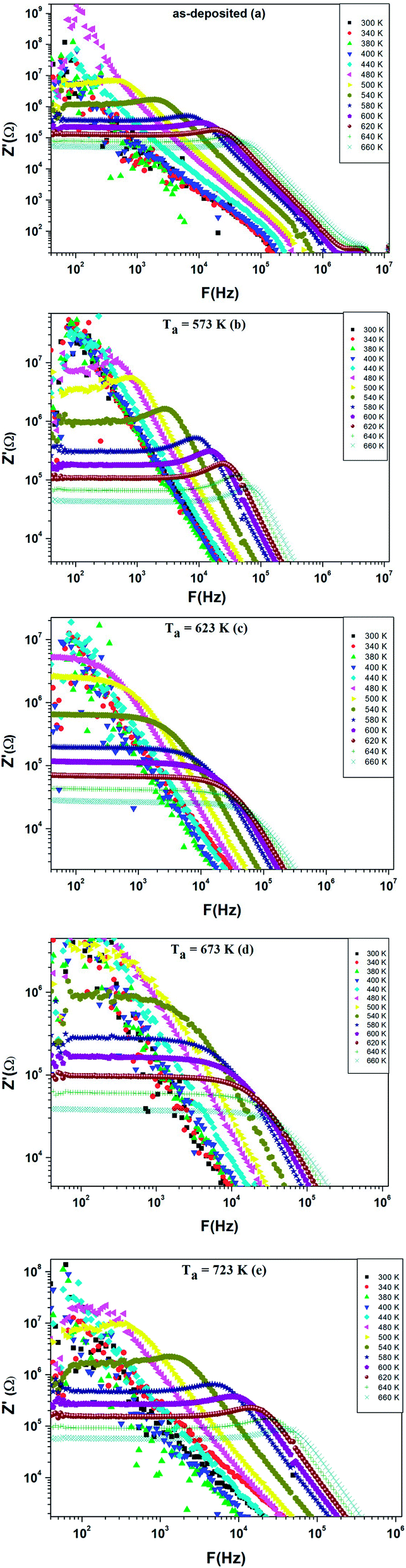
Additionally, Fig. 10(a–e) shows the frequency dependence of the conductance G at different temperatures (300–660 K) for as-deposited and different annealed films of ZnS in the frequency range 40–106 Hz.
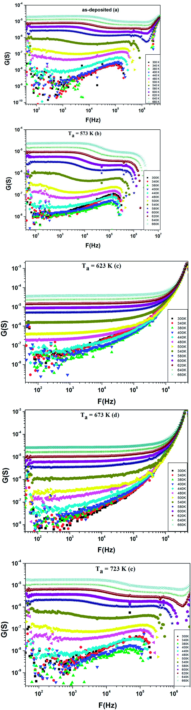 | ||
| Fig. 10 Frequency dependence of ac conductance for ZnS films annealed at different temperatures. | ||
We can notice from Fig. 10(a) and (b) that the profile of the total conductance exhibits many regimes. At low frequency, the conductance has a small variation with frequency and increased with temperature. This rise of conductance with temperature indicates that the conduction process in the material is thermally activated. This regime is followed by a metal behavior where the conductance decreases with frequency. Finally, an insulator behavior appears at high frequency. The same behavior was observed for films annealed at T = 723 K (Fig. 10(e)). On the other hand, we observe from Fig. 10(c and d) that these spectra are composed by two regions. One at low frequency: the spectrum is characterized by the appearance of a plateau for each temperature. However, the second one is at high frequency, where the conductance G increases linearly in logarithmic scale with frequency. For these two samples, the conductance G can be described using the Jonscher power law:41
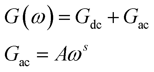 | (2) |
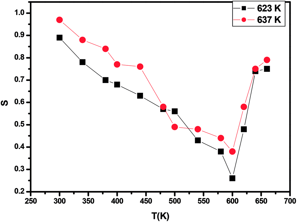 | ||
| Fig. 11 Variation of frequency exponent (s) with temperature of annealed ZnS films at 623 K and 673 K. | ||
For the quantum mechanical tunneling (QMT) model,42 the frequency exponent s is in order of 0.8 and increases slightly with increasing temperature or is independent of temperature. Therefore, (QMT) model is not suited to the investigated film samples annealed at 623 K and 673 K. In the correlated barrier hopping (CBH) model,43 the obtained values of s decrease continuously with increasing temperature. Hence, (CBH) model cannot explain the obtained results too.
However, in the overlapping large polaron tunnelling (OLPT) model,44 the exponent s is both temperature and frequency dependent and it has reached minimum value at a certain temperature before continuing to increase with increasing temperature. Consequently, the (OLPT) model is in good agreement with the obtained results. We must note that to our knowledge the (OLPT) conduction mechanism ensured by large polarons has been rarely obtained for chalcogenide materials. We point out that when the polaron energy is derived from polarization changes in the deformed lattice, which is the case of ionic crystals, the corresponding excitation is named large or dielectric polaron.45 We can thus deduce that the annealing process to a certain value of the temperature (which allows us to obtain a certain degree of crystallinity of this amorphous material) is at the origin of the reinforcement of the polarization behavior of the material and thus the appearance of the (OLPT) conduction mechanism.
The plot of log(GdcT) versus 1000/T for annealed ZnS films at Ta = 623 K is linear over a wide temperature range justifying that conductivity is thermally activated and can be expressed by Mott and Davis law (Fig. 12):46
 | (3) |
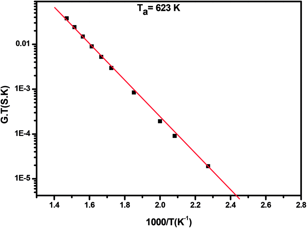 | ||
| Fig. 12 Variation of log(GdcT) as a function of (1000/T) for annealed ZnS films ZnS at Ta = 623 K. | ||
| Ea (eV) (dc conductance) | Ea (eV) (dielectric relaxation) | |
|---|---|---|
| As-deposited | 863 | 839 |
| 300 °C | 832 | 783 |
| 350 °C | 810 | 807 |
| 400 °C | 818 | 744 |
| 450 °C | 907 | 860 |
These results are correlated to the XRD ones. Both as grown sample and 573 K annealed one (group A) have an amorphous structure and exhibit both metallic and insulator behavior. When annealing temperature increases (Ta = 623 K and 673 K, group B), crystalline phase begins to appear and the conductance follows the Jonsher law. Finally, for sample annealed at 723 K (group C) the crystalline phase dominates and complex regime appears for the conductance. Such correlation and evolution can be argued as follow: for group A samples contain defects which emit free carriers at different frequencies. This increases the density of free carriers and the conductance follows the Drude model. When all defects become empty of free carriers, the hopping model takes place. For group B, thermal annealing cures samples from defects and nucleates crystallites and this yields to a homogenous insulating material. For group C, we notice an increase in grain size which could affect the conductance. Sulfur content, which varies with annealing temperature, could be at the origin of defects which affect the conductance.
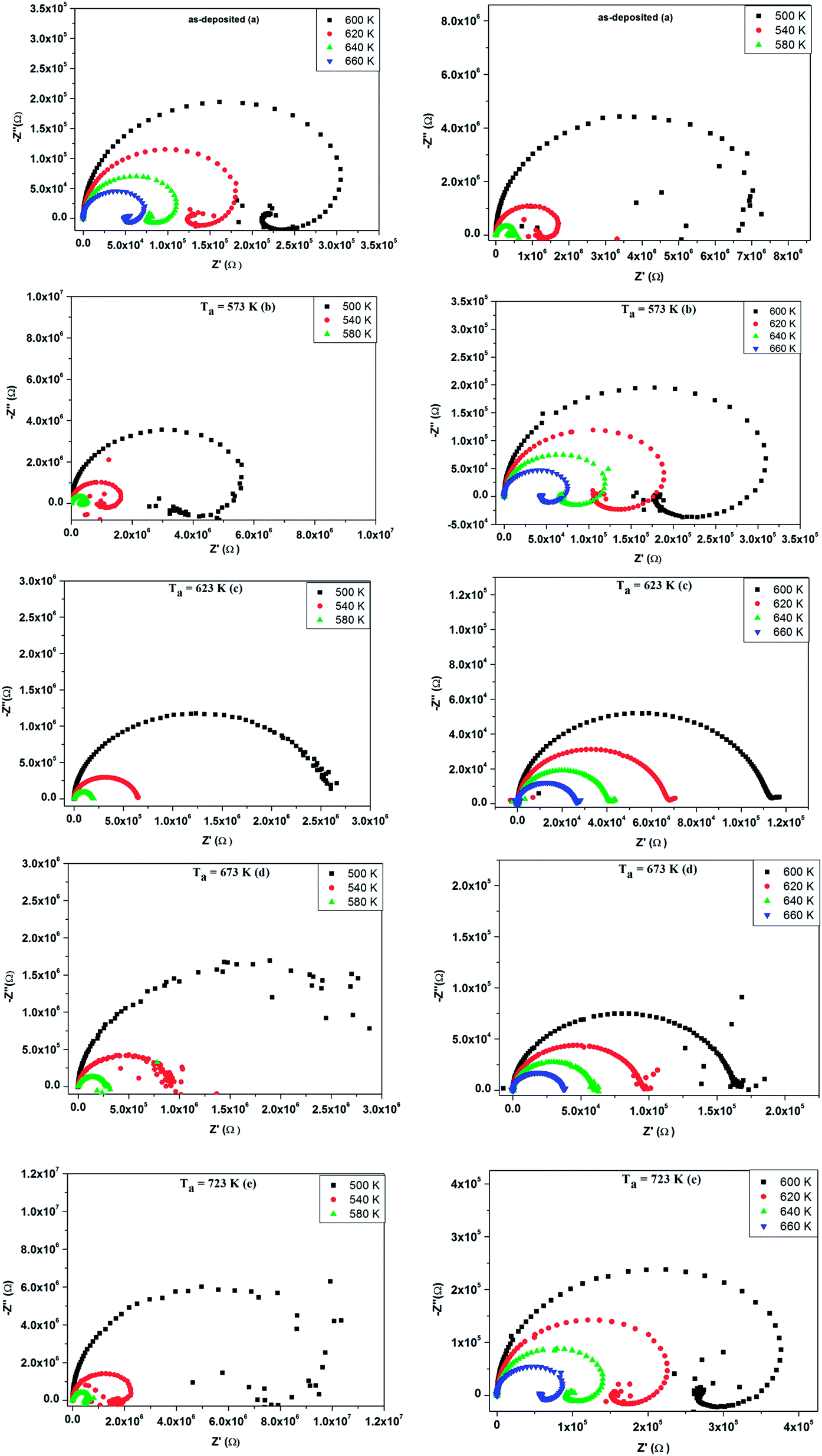 | ||
| Fig. 13 (a–e) Complex impedance spectrum (−Z′′ vs. Z′) of as-deposited and annealed ZnS films at 573–723 K. | ||
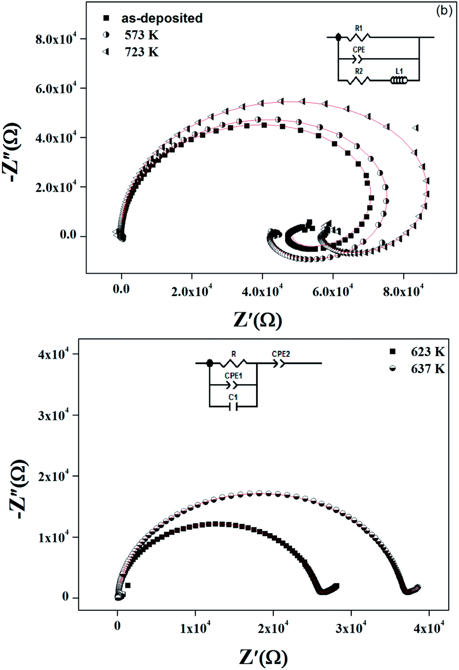 | ||
| Fig. 14 Nyquist plots at 660 K for as-deposited and annealed ZnS films. Inset shows the proposed model for different annealed ZnS thin films. | ||
The occurrence of an inductive loop at low frequencies implies the presence of metallic phase which could be due to the free carrier emitter for group A. It is usually associated to the relaxation of adsorbed anions or to nanostructure materials.50–53 The studied films evaluate from amorphous structure to nanocrystalline one as annealing temperature increases. For the as grown sample and the one annealed at 573 K, the films could contain small quantities of secondary phases of ZnS1−x(OH)x, Zn(OH)2 and ZnSO4.54 Such phases shorten the band gap55 and induce metallic conduction pathway. The capacitive behavior is then replaced by an inductive one. After an annealing at a temperature of 723 K, a nanocrystalline phase appears and it is known that electrical conductivity is grain size dependent.56 When the grain size increases the mean electron free path increases and the grain boundary scattering decreases. Nanocrystalline grain could percolate, inducing a conductive pathway which involves the inductive behavior. For samples, annealed at 623 K and 723 K, the secondary phases are desorbed and the films have the insulator behavior. This explanation is in agreement with the variation of the conductance with the frequency in Fig. 10, the XRD patterns of Fig. 2, the AFM and SEM images of Fig. 3 and 4, respectively. So the significant change of Nyquist plot with annealing temperature permits the correlation between the microstructure and its electrical properties.
Fig. 15 exhibits the variation of real part of the impedance Z′ with frequency at different temperatures for as deposited and different annealed ZnS films. It is noted that Z′ have a high values for low temperatures and decreases with increase in frequency, thus indicating an increase in ac conductivity with rise in frequency. We observe that the magnitude of Z′ decreases sharply for both annealed ZnS thin films at 623 K and 673 K. This result confirms the increase of conductance observed in Fig. 10(c and d).
 | ||
| Fig. 15 Variation of the real part Z′ of impedance as a function of frequency at different temperatures for ZnS films annealed at various temperatures. | ||
The variation of imaginary part of impedance (Z′′) with frequency at different temperatures was depicted in Fig. 16. The spectra are characterized by appearance of peaks, which shift to higher frequencies with the increase of temperature. Such behavior points out the presence of relaxation phenomena in the system.41 Also we observe that the magnitude of Z′′ decreases gradually when the temperature increases. This is due to the accumulation of electrical charges in the material. It is clearly visible in Fig. 15 that both annealed films at 623 K and 673 K have a significant broadening of the peaks of Z′′, which confirms that the relaxation process in the compound is temperature dependent.57 The maximum of the relaxation peaks decreases with the increment in temperature, indicating the drop in the resistive properties.58 Hence, it can be concluded that in the both annealed films at 623 K and 673 K the relaxation process is well pronounced.
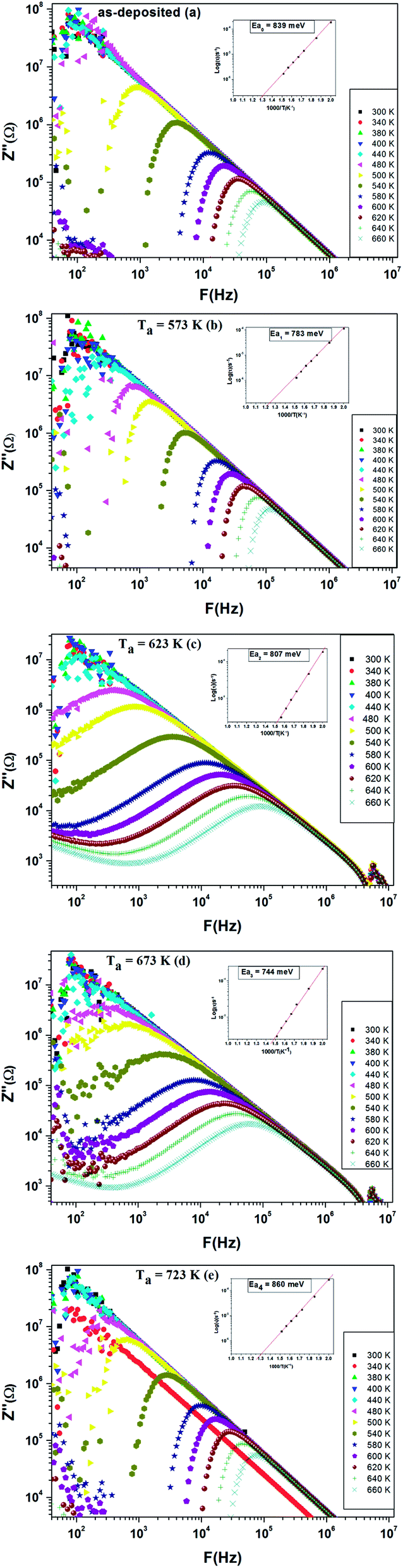 | ||
| Fig. 16 Variation of the imaginary part Z′′ of impedance as a function of frequency at different temperatures for ZnS films annealed at various temperatures. The Arrhenius plot of time relaxation is shown in the inset of each figure. | ||
Furthermore, the relaxation time τ of the electrical phenomena in the material was evaluated by using the impedance data of Z′′. The typical variation of τ as a function of temperature is depicted in the inset of each figure. Experimental data can be fitted by a linear law at high temperature. The different activation energy values are reported in Table 2. It is obvious that the activation energy deduced from relaxation time is very close to the value estimated from conductance spectrum, which indicates that relaxation process and conductivity have the same origin.
4. Conclusion
ZnS thin films were grown annealed in the temperature range (573–723 K). The as-deposited and annealed films at Ta < 673 K were amorphous, while those annealed at Ta ≥ 673 K show hexagonal phase of ZnS with preferred orientation (002). The increase in the annealing temperature enhances the crystallinity of ZnS films and increases the grain size. At a high annealing temperature (723 K), the surface roughness of annealed films becomes more than nine fold if compared to as-deposited film. The EDS analysis proves that the annealed ZnS thin film has Zn-rich and S-deficient composition. The electrical conductance improves with increasing annealing temperature up to 623 K and then this improvement was declined. The ZnS films annealed at 623 K had the highest conductance and the lowest activation energy. The ac conductance obeys to the universal power law and can qualitatively be described by the OLPT model for films annealed at 623 K and 673 K. According to our bibliography, we have rarely found this mechanism of conduction in chalcogenides. Generally, ac conduction in these types of materials is managed by the (CBH) and the small polaron tunneling (SPT) mechanisms. The appearance of this conduction mechanism for chalcogenides may be due the ionic nature of ZnS and to the effect of annealing, which allows the amorphous material to reach a certain degree of crystallinity. The dielectric constant and dielectric loss of the samples were found to decrease with increasing frequency and increase with increasing temperature. Thus, dependences of the ac conductance, the dielectric constant and the dielectric loss on frequency and temperature were possible. In addition to that, the dielectric behavior was associated to the polarization effect. An improvement on the dielectric constant ε′ and dielectric loss ε′′ with annealing was noticed. The impedance plots were in good accordance with the conductance plots. The activation energy deduced from dc conductance and relaxation time are in good agreement, which indicates that both processes are related to the same mechanism of conduction. The post annealing leads to an improvement in the crystallinity and the conductance of ZnS films will be useful for the formation of ZnS based heterostructure for the application of optoelectronic devices. XRD, AFM and impedance spectroscopy analysis reveal that the best annealing temperature for obtaining a good ZnS hexagonal structure film is 723 K.Conflicts of interest
There are no conflicts to declare.Acknowledgements
This work was supported by Tunisian Ministry of Higher Education and Scientific Research, Spanish Ministry of Science and Innovation – FEDER Funds (MODENA Project CTQ2016-79461-R) and Fundación Ramón Areces (Spain, Project CIVP18A3940). NANOMAG group belongs to Galician Competitive Research Group ED431C-2017/22, programme co-funded by FEDER, and AEMAT Strategic Partnership (ED431E-2018/08, Xunta de Galicia, Spain).References
- M. H. Suhail, I. M. Al Essa and R. A. Ahmed, International Journal of Engineering and Technical Research, 2014, 2, 9 Search PubMed.
- H. Wang, X. Lu, Y. Zhao and C. Wang, Mater. Lett., 2006, 60, 2480 CrossRef CAS.
- N. Habubi, M. Hashim and A. Al-Yasiri, Baghdad Sci. J., 2010, 7, 1421 Search PubMed.
- J. S. Jie, W. J. Zhang, I. Bello, Ch. S. Lee and S. T. Lee, Nano Today, 2010, 5, 313 CrossRef CAS.
- L. W. Ji, Y. J. Hsiao, I. T. Tang, T. H. Meen, Ch. H. Liu, J. K. Tsai, T. Ch. Wu and Y. S. Wu, Nanoscale Res. Lett., 2013, 8, 1 CrossRef PubMed.
- M. Nematollahi, X. Yang, L. M. S. Aas, Z. Ghadyani, M. Kildemo, U. J. Gibson and T. W. Reenaas, Sol. Energy Mater. Sol. Cells, 2015, 141, 322 CrossRef CAS.
- J. Kim, C. Park, S. M. Pawar, A. I. Inamdar, Y. Jo, J. Han, J. Hong, Y. S. Park, D. Y. Kim, W. Jung, H. Kim and H. Im, Thin Solid Films, 2014, 566, 88 CrossRef CAS.
- T. Kryshtab, V. S. Khomchenko, V. B. Khachatryan, N. N. Roshchina, J. A. Andraca-Adame, O. S. Lytvyn and V. I. Kushnirenko, J. Mater. Sci.: Mater. Electron., 2007, 18, 1115 CrossRef CAS.
- Y. G. Yoon and I. H. Choi, J. Korean Phys. Soc., 2013, 63, 1609 CrossRef CAS.
- A. U. Ubale, V. S. Sangawar and D. K. Kulkarni, Bull. Mater. Sci., 2007, 30, 147 CrossRef CAS.
- Y. M. Yu, M. H. Hyun, S. Nam, D. Lee, O. Byungsung, K. S. Lee, P. Y. Yu and Y. D. Choi, J. Appl. Phys., 2002, 91, 9429 CrossRef CAS.
- X. Wang, J. Shi, Z. Feng, M. Li and C. Li, Phys. Chem. Chem. Phys., 2011, 13, 4715 RSC.
- S. S. Kumar, M. A. Khadar, K. G. M. Nair, S. Dhara and P. Magudapathy, J. Raman Spectrosc., 2008, 39, 1900 CrossRef CAS.
- J. H. Yu, J. Joo, H. M. Park, S. I. Baik, Y. W. Kim, S. C. Kim and T. Hyeon, J. Am. Chem. Soc., 2005, 127, 5662 CrossRef CAS PubMed.
- M. A. Rahman, M. R. Phillips and C. Ton-That, J. Alloys Compd., 2016, 691, 339 CrossRef.
- W. Naffouti, T. Ben Nasr, N. Battaglini, S. Ammar and N. Turki-Kamoun, J. Renewable Sustainable Energy, 2015, 7, 063132 CrossRef.
- A. Tecaru, A. I. Danciu, V. Musat, E. Fortunato and E. Elangovan, J. Optoelectron. Adv. Mater., 2010, 12, 1889 CAS.
- B. S. Yun and J. Kim, J. Korean Phys. Soc., 2008, 53, 331 CrossRef CAS.
- R. Jeyachitra, V. Senthilnathan and D. Kathirvel, Int. J. ChemTech Res., 2014, 6, 3152 Search PubMed.
- N. Shanmugam, S. Cholan, N. Kannadasan, K. Sathishkumar and G. Viruthagiri, J. Nanomater., 2013, 2013, 351798 Search PubMed.
- E. M. N. Al-Fawade, I. S. Naji and H. I. Mohammed, Ibn Al-Haitham Journal for Pure and Applied Science, 2012, 25, 150–161 Search PubMed.
- R. Jeyachitra, V. Senthilnathan and D. Kathirvel, Int. J. ChemTech Res., 2014, 5, 3152–3159 Search PubMed.
- N. Bouguila, D. Bchiri, M. Kraini, A. Timoumi, I. Halidou, K. Khirouni and S. Alaya, J. Mater. Sci.: Mater. Electron., 2015, 26, 9845 CrossRef CAS.
- B. D. Cullity, Elements of X-ray Diffraction, Addison-Wesley, Reading, MA, 1978 Search PubMed.
- A. A. Ziabari and F. E. Ghodsi, Mater. Sci. Semicond. Process., 2013, 16, 1629 CrossRef.
- X. D. Gao, X. M. Li and W. D. Yu, Thin Solid Films, 2004, 468, 43–47 CrossRef CAS.
- F. Ouachtari, A. Rmili, S. Elidrissi, A. Bouaoud, H. Erguig and Ph. Elies, J. Mod. Phys., 2011, 2, 7152 Search PubMed.
- H. Lashgari, A. Boochani, A. Shekaari, S. Solaymani, E. Sartipi and R. T. Mendi, Appl. Surf. Sci., 2016, 369, 76 CrossRef CAS.
- M. A. Khans and N. Bouarissa, Optik, 2010, 124, 5095 CrossRef.
- M. M. El-Desoky, M. A. Ali, G. Afifi, H. Imam and M. S. Al-Assiri, Silicon, 2018, 10, 301–307 CrossRef CAS.
- Ch. Rayssi, S. El. Kossi, J. Dhahri and K. Khirouni, RSC Adv., 2018, 8, 17139 RSC.
- P. R. Das, L. Biswal, B. Behera and R. N. P. Choudhary, Mater. Res. Bull., 2009, 44, 1214–1218 CrossRef CAS.
- K. Omri and R. Lahouli, J. Mater. Sci.: Mater. Electron., 2019, 30, 7834–7839 CrossRef CAS.
- T. S. Sasikala, C. Pavithran and M. T. Sebastian, J. Mater. Sci.: Mater. Electron., 2010, 21, 141–144 CrossRef CAS.
- P. Nayak, T. Badapanda, A. K. Singh and S. Panigrahi, RSC Adv., 2017, 7, 16319–16331 RSC.
- B. N. Parida, P. R. Das, R. Padhee and R. N. P. Choudhary, J. Alloys Compd., 2012, 540, 267 CrossRef CAS.
- N. Panda, B. N. Parida, R. Padhee and R. N. P. Choudhary, J. Mater. Sci.: Mater. Electron., 2015, 26, 3797 CrossRef CAS.
- A. J. Haider, A. M. Mousa and S. M. H. Al-Jawad, J. Semicond. Tech. Sci., 2008, 8, 326 CrossRef.
- T. R. Gopalarao, S. Ravi and D. Pamu, J. Supercond. Novel Magn., 2015, 28, 1571–1576 CrossRef CAS.
- K. S. Ramaiah, R. D. Pilkington, A. E. Hill, R. D. Tomlinson and A. K. Bhatnagar, Mater. Chem. Phys., 2001, 68, 22–30 CrossRef CAS.
- A. K. Jonscher, Nature, 1977, 267, 673 CrossRef CAS.
- A. Ghosh, Phys. Rev. B, 1990, 41, 1479 CrossRef CAS.
- S. R. Elliott, Philos. Mag. B, 1977, 36, 1291 CrossRef CAS.
- E. V. Gopalan, K. A. Malini, S. Sagar, D. S. Kumar, Y. Yoshida, I. A. Al-Omari and M. R. Anantharaman, J. Phys. D: Appl. Phys., 2009, 42, 165005 CrossRef.
- A. R. Long, Adv. Phys., 1982, 31, 553 CrossRef CAS.
- N. F. Mott and E. A. Davis, Electronic Process in Non-crystalline Materials, Clarendon Press, Oxford, 1979 Search PubMed.
- R. Vaish and K. B. R. Varma, Ionics, 2011, 17, 727 CrossRef CAS.
- Aakansha, B. Deka, S. Ravi and D. Pamu, Ceram. Int., 2017, 43, 10468 CrossRef CAS.
- I. Trabelsi, A. Jebali and M. Kanzari, J. Mater. Sci.: Mater. Electron., 2016, 27, 4326 CrossRef CAS.
- J. Suchanicz, Mater. Sci. Eng., B, 1998, 55, 114 CrossRef.
- M. C. Fatah, M. C. Ismail, B. Ari-Wahjoed and K. A. Kurnia, Mater. Chem. Phys., 2011, 127, 347 CrossRef CAS.
- J. Datta, C. Bhatacharya and S. Bandyopadhyay, Bull. Mater. Sci., 2005, 28, 253 CrossRef CAS.
- K. A. Z. Syed Abuthahir and R. Jagannthan, Mater. Chem. Phys., 2010, 121, 184 CrossRef.
- G. Markovitch, C. P. Collier and J. R. Heath, Phys. Rev. Lett., 1998, 80, 3807 CrossRef.
- M. H. Doha, M. J. Alam, J. Rabeya, K. A. M. H. Siddiquee, S. Hussain, O. islam, M. A. Gafur, S. Islam, N. Khatun and S. H. Sarkar, Optik, 2015, 126, 5194 CrossRef CAS.
- R. S. S. Saravanan, D. Pukazhselvan and C. K. Mahadevan, J. Alloys Compd., 2012, 517, 139 CrossRef CAS.
- M. Nadeem and M. J. Akhtar, J. Appl. Phys., 2008, 104, 103713 CrossRef.
- M. Younes, M. Nadeem, M. Atif and R. Grossinger, J. Appl. Phys., 2010, 109, 93704 CrossRef.
| This journal is © The Royal Society of Chemistry 2020 |