
 Open Access Article
 This Open Access Article is licensed under a Creative Commons Attribution-Non Commercial 3.0 Unported Licence
Composite formation in CdSe:Cu2Se nanocrystal films, charge transport characteristics and heterojunction performance†
N. Sajid Babu and
M. Abdul Khadar‡
*
and
M. Abdul Khadar‡
*
Department of Nanoscience and Nanotechnology, University of Kerala, Kariavattom, Thiruvananthapuram 695 581, Kerala, India. E-mail: mabdulkhadar@rediffmail.com
First published on 2nd March 2020
Abstract
The use of nanocrystals as materials for potential technological applications depends on tailoring their properties through intentional doping with external impurities. We have used a new technique to synthesize nanocrystal thin films of CdSe:Cu2Se containing different weight percentages (wt%) of Cu2Se. The films were deposited on glass substrates at room temperature by co-evaporation of CdSe and Cu2Se powder in nitrogen gas at a pressure larger than that required for conventional thin film deposition. The films consisted of nanograins of CdSe doped with Cu2Se (i.e., nanograins of Cd1−xCu2(x)Se where x is the atom% of Cu2Se doped into CdSe) for lower wt% of Cu2Se, and nanocomposites of Cd1−xCu2(x)Se and Cu2Se for higher wt% of Cu2Se. An energy band diagram built using the Anderson model was used for discussing the heterojunction characteristics of the junction between nanograins of Cd1−xCu2(x)Se and Cu2Se. To investigate the usefulness of the nanocrystal thin films of CdSe:Cu2Se for practical applications, the I–V characteristics of p–p and p–n hetero-junctions formed by the films respectively with nanostructured films of similarly deposited Cu2Se and CdSe films were studied.
Introduction
Semiconductor nanocrystals (NC) exhibit interesting size dependent properties which markedly deviate from their bulk properties, but additional control of these properties is required for their practical applications. The use of nanocrystals as materials for potential technological applications depends on tailoring their properties through intentional doping with external impurities. In the case of bulk semiconductors, under thermal equilibrium determined by Gibbs free energy and growth temperature, impurity atoms can be incorporated up to their solid solubility limit which can be as much as 50% for II–VI semiconductors. But the addition of only a few dopant atoms into nanomaterials, quantum dots (QDs), can make them heavily doped and doping foreign atoms into quantum dots is a challenging problem.1–5 When doping of a semiconductor with another material is attempted, the dopant in excess of the quantity that gets incorporated into the semiconductor through doping would separate out as a second phase resulting in the formation of a composite of the doped semiconductor along with the dopant. The desirable properties of different nanoscale building blocks can be combined through the synthesis of their nanocomposites which offer an opportunity for creating materials with tailored properties for the fabrication of devices for specific applications. Nanocomposites of n- and p-type semiconductors are of importance for technological applications in optoelectronic devices including photovoltaics.5 Synthesis of nanocomposites such as metal–metal,6 metal–polymer,7 metal–dielectric,8 dielectric–metal,9 semiconductor–polymer,10 semiconductor–dielectric,11 and semiconductor–semiconductor12 in different morphologies like powders, mesocrystals and films for specific applications have been reported. For practical applications such a solar cells, nanocomposites are required in the form of films it would be advantageous if the components of the nanocomposite are in the nanosize regime. These requirements necessitate that both the components of a two phase nanocomposite should be generated as nanoparticles which deposit simultaneously on substrates to form of nanostructured films with non-resistive inter-particle contacts. Nanu et al.13 used atomic layer chemical vapour deposition to infiltrate CuInS2 inside the pores of nanostructured TiO2 to prepare nanocomposite of n-type TiO2 and p-type CuInS2. Beal et al.14 employed radio frequency sputtering to produce CdTe–ZnO nanocomposite thin films with varied semiconductor-phase extended structures and studied the optical absorption and the carrier transport behaviour of these films. Potter et al.15 used a dual-source, sequential radio-frequency sputter deposition technique to study the spatial distribution of CdTe nanoparticles within ZnO thin-film matrix.Nanostructured films of doped semiconductors and nanocomposites have received much attention recently because of their unique electronic16–18 and optical properties,19 and important applications such as photochemical solar cells20 transparent conductive films21 laser diodes22 and in magnetic storage devices.23–25 CdSe is an important II–VI semiconductor and has been extensively investigated for studying quantum size effects in semiconductor quantum structures.26–28 Zhang et al.29 through theoretical studies predicted that CdSe can easily be n-doped and lightly p-doped. Cu2Se is a p-type semiconductor due to copper vacancies and has an indirect band gap of 1.1–1.27 eV![[thin space (1/6-em)]](https://www.rsc.org/images/entities/char_2009.gif) 30 which makes it an absorber material and a direct bandgap between 2.0 and 2.3 eV which makes it a window material in solar cells.31–33 P-type doping of CdSe with Cu2Se can tune the bandgap of CdSe for varying its optical response and this can improve the photocurrent conversion efficiency by providing extra holes. Simi et al.34 reported the synthesis of type II core–shell quantum dots by a high temperature organometallic method. They inferred that the charge separation in the CdSe–Cu2Se core–shell system makes it a good choice for designing light harvesting devices. Xu et al.35 synthesized (CuS)x:(ZnS)1−x (x = 1 to x = 0) nanocomposite system with the aim of maximizing both transparency and hole conductivity and found that the hole conductivity was linked to the proportion of the CuS phase.
30 which makes it an absorber material and a direct bandgap between 2.0 and 2.3 eV which makes it a window material in solar cells.31–33 P-type doping of CdSe with Cu2Se can tune the bandgap of CdSe for varying its optical response and this can improve the photocurrent conversion efficiency by providing extra holes. Simi et al.34 reported the synthesis of type II core–shell quantum dots by a high temperature organometallic method. They inferred that the charge separation in the CdSe–Cu2Se core–shell system makes it a good choice for designing light harvesting devices. Xu et al.35 synthesized (CuS)x:(ZnS)1−x (x = 1 to x = 0) nanocomposite system with the aim of maximizing both transparency and hole conductivity and found that the hole conductivity was linked to the proportion of the CuS phase.
In the present work, we have used a new technique to synthesize nanocrystal thin films of CdSe:Cu2Se containing different weight percentages (wt%) of Cu2Se. In this technique, the films were deposited on glass substrates at room temperature by co-evaporation of CdSe and Cu2Se powder in nitrogen gas using a vacuum coating unit at a pressure larger than that required for conventional thin film deposition. While the constituent phases of a composite can be precisely determined using X-ray diffraction, the substitutional incorporation of a dopant into the host lattice can also be known through X-ray diffraction since the intensity of a diffraction peak depends on the structure factor which depends on the distribution of atoms on the set of plane responsible for the peak. Because of the influence of deposition process, the synthesized films consisted of nanograins of CdSe doped with Cu2Se (i.e., nanograins of Cd1−xCu2(x)Se where x is the atom% of Cu2Se doped into CdSe) for lower wt% of Cu2Se, and nanocomposites of Cd1−xCu2(x)Se and Cu2Se for higher wt% of Cu2Se. The electrical conductivity of the CdSe:Cu2Se thin films was found to be improved due to the p-type doping with Cu2Se. Energy band diagram built using the Anderson model considering the films to be made up of nanocomposites of nanograins of Cd1−xCu2(x)Se and Cu2Se for higher wt% of Cu2Se was used for discussing the heterojunction characteristics of the junction between nanograins of Cd1−xCu2(x)Se and Cu2Se, for the first time. To investigate the usefulness of nanocrystal thin films of CdSe:Cu2Se for practical applications such as solar cells, the I–V characteristics of p–p and p–n heterojunctions formed by the films respectively with nanostructured films of similarly deposited Cu2Se and CdSe films were studied.
Experimental
Nanocrystal thin films of CdSe:Cu2Se were deposited on glass substrates by thermal evaporation of CdSe and Cu2Se powders for different wt% of Cu2Se. Glass substrates were cleaned with detergent, etched for 5 min in dilute nitric acid, degreased with methanol and ultrasonically cleaned with acetone and then dried in hot air before deposition of the films. The cleaned substrates were then dried in hot air. Depositions of the films were carried out not at high vacuum but at an appreciably high pressure of nitrogen gas (99.99%) of ∼1 × 10⁻⁴ mbar which was much larger than the vacuum required for thin film deposition. On evaporating CdSe and Cu2Se powders, supersaturation of the nitrogen gas with vapours of these materials produced nanoparticles which deposited on the substrates as nanostructured thin films of CdSe:Cu2Se. Nanostructured films were deposited for different wt% of 5, 10, 20 and 30% of Cu2Se. The film samples were assigned the sample codes CS5, CS10, CS20, and CS30 where the number after CS denotes the doping percent of Cu2Se.The crystallinity, crystal structure and growth orientation of the film samples were investigated using X-ray diffraction (XRD). A Bruker AXS D8 advance X-ray diffractometer equipped with Kristalloflex 780, KF. 4KE X-ray source (λ ∼ 1.5406 Å) was used to record the XRD pattern of the samples. The average thickness of the film samples was measured using a Bruker Dektak-XT stylus profiler. Energy Dispersive Spectroscopy (EDS) measurements were performed using JEOL Model JED-2300 Energy Dispersive Spectrometer. AFM measurements were carried out on the film samples using a Digital Instruments Nanoscope-E and using a Si3N4 100 μm cantilever having a force constant of 0.58 N m−1 in contact mode. The optical transmission spectrum of the film sample was recorded using a JASCO V-650 double beam spectrophotometer at room temperature. Raman measurements on the sample were performed using Jobin Yvon Horiba Labram – HR 800 micro-Raman spectrometer with a He–Ne laser (633 nm) as the excitation source. XPS measurements were done using ESCA Instrument: VSW, UK with a Resolution: ∼1 eV, source: Al K alpha X-rays.
For DC and photoconductivity measurements, silver coplanar electrodes were painted at a separation of 2 mm on the surface of the films deposited on glass substrates. Electrical measurements on the samples were carried keeping the samples in a cell at a vacuum of ∼0.001 mbar. Ohmic nature of the contacts of the electrodes with the sample was verified from I–V measurements using a Keithley 2400 source meter. The resistance of the samples was measured using a standard DC two point probe method over the temperature range from 300 to 423 K with an applied voltage of 3 V corresponding to the ohmic region of the I–V plot. The dc conductivity (σ) was determined using the relation,  The resistivity ρ was calculated as
  where R is the resistance, b is the distance between the electrodes, t the thickness and l is the length of the electrodes. Hall measurements were carried out on the samples CS20 and CS30 using PPMS (Quantum Design DynaCool) (the samples CS5 and CS10 were too resistive for Hall measurements). After loading the sample of 4 × 8 mm size on the sample holder, a linearity check was performed to confirm the ohmic behaviour of the electrical contacts. To investigate the usefulness of nanocrystal thin films of CdSe:Cu2Se for practical applications, the I–V characteristics of homo and heterojunctions formed by the films respectively with nanostructured thin films of similarly synthesized CdSe and Cu2Se films were measured.
Results and discussion
The XRD patterns of nanocrystal thin films of pure CdSe, and of CdSe:Cu2Se containing different Cu2Se wt% of 5, 10, 20 and 30% are shown in Fig. 1. The EDS spectrum of CdSe:Cu2Se nanostructured thin film sample containing 10 wt% of Cu2Se is shown in Fig. S1† and the atom% (at%) of Cd and Cu in the film samples are given in Table S1.† The at% of Cu in the film samples CS5, CS10, CS20 and CS30 were ∼4, ∼9, ∼18 and ∼30 respectively. The XRD pattern of the sample CS5 shows a strong peak at 2θ value of 25.4° corresponding to the (002) reflection and weak peaks at 2θ values of 24° and 42° corresponding to the (100) and (110) reflections of CdSe of hexagonal phase (ICDD file no. 01-071-4772). The XRD pattern shows no peaks corresponding to Cu2Se even though EDS analysis results showed the presence of Cu2Se in the sample leading to the inference that Cu2Se got doped into CdSe lattice through replacement of Cd by Cu. The XRD pattern of the sample containing 10 wt% of Cu2Se (CS10) shown in Fig. 1(c) is identical with the pattern of CS5 in Fig. 1(b) indicating that the sample CS10 also does not contain Cu2Se as a separate phase but it got incorporated into CdSe through doping. In the XRD patterns of the samples CS20 in Fig. 1(d), in addition to the (002), (100) and (110) peaks of CdSe, a weak peak like feature at 2θ value of 26.78° is observed, while in the XRD pattern of the sample CS30 in Fig. 1(e) a weak peak is observed at 2θ value of 26.78° in addition to the CdSe peaks. The peak at 26.78° was identified as the (111) reflection of Cu2Se (ICDD file no. 03-065-2982) showing that Cu2Se existed as a separate phase in the samples CS20 and CS30. The intensity of this peak increased in the pattern of CS30 in Fig. 1(e) compared to that in Fig. 1(d) of the sample CS20. From the XRD results it was inferred that the samples CS20 and CS30 are CdSe:Cu2Se nanocomposites with some percentage of Cu2Se doped into the CdSe lattice.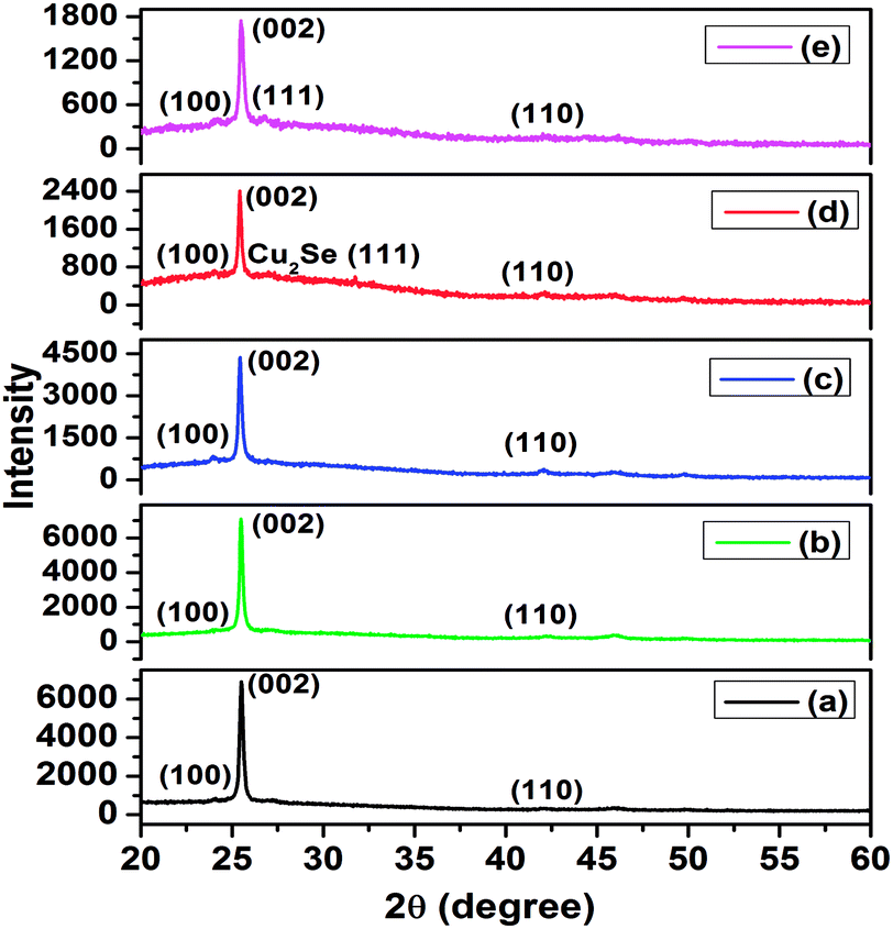 | ||
| Fig. 1 XRD patterns of nanocrystal thin films of (a) pure CdSe, and of CdSe:Cu2Se containing different concentrations of Cu2Se: (b) 5 wt%, (c) 10 wt%, (d) 20 wt% and (e) 30 wt%. | ||
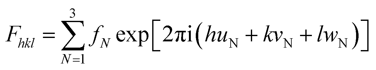
From the XRD results, it is possible to derive information on the nature of incorporation of Cu2Se into the nanocrystal thin films of CdSe:Cu2Se samples. The substitutional incorporation of dopant atoms in a host material would affect the atomic scattering factor and the structure factor causing a change in the relative intensities of the diffraction peaks.16 From Fig. 2(a), it is clear that the intensity of the (002) peak of CdSe decreased with increase in the concentration of Cu2Se incorporated in the samples. The decrease in intensity of (002) plane is due to the incorporation of Cu2Se into the CdSe:Cu2Se samples. Table 1 shows that the thickness of the film samples increased with an increase in wt% of Cu2Se. Hence, the decrease in the intensity of the (002) peak in the XRD pattern is not due to decrease in the mass of the material scattering the X-rays but is due to decrease in the scattering power of the material of the samples with the increase in the wt% of Cu2Se. The atomic scattering factor is equal to the number of electrons in each atom and is 48 and 29 for Cd and Cu, respectively. Hence, the replacement of Cd2+ by two numbers of Cu1+ may be expected to decrease the intensity of a particular XRD peak depending on the structure factor.36,37 The intensity of (hkl) peak in the XRD pattern of a material is represented by the structure factor (F) given by:
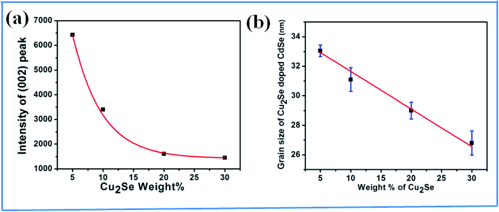 | ||
| Fig. 2 (a) Plot of XRD intensity of (002) peak of CdSe with Cu2Se wt%; (b) plot of variation of grain size of CdSe in the nanocrystal thin films of CdSe:Cu2Se with wt% of Cu2Se. | ||
| Sl no. | Sample code | Composition (CdSe:Cu2Se) |
Thickness (nm) | Grain size of Cu2Se doped CdSe nanoparticles (nm) | Bandgap energy (eV) | |
|---|---|---|---|---|---|---|
| Eg1 (CdSe) | Eg2 (Cu2Se) | |||||
| 1 | CS5 | 95:5 |
104 | 33.0 ± 0.4 | — | 1.85 ± 0.01 |
| 2 | CS10 | 90:10 |
110 | 31.0 ± 0.8 | 1.77 ± 0.01 | 1.99 ± 0.04 |
| 3 | CS20 | 80:20 |
162 | 29.0 ± 0.6 | 1.80 ± 0.01 | 2.07 ± 0.02 |
| 4 | CS30 | 70:30 |
223 | 26.8 ± 0.8 | 1.90 ± 0.03 | 2.08 ± 0.03 |
The (002) peaks of all the samples are enlarged and shown together in Fig. S2.† Fig. S2† shows that the (002) peak shifted towards lower 2θ values for lower Cu2Se doping wt% and then shifted to larger 2θ values for higher concentrations of Cu2Se. The shift towards lower 2θ values is attributed to the shrinkage of CdSe crystal lattice due to the substitution of Cd2+ ions of the larger ionic radius (0.078 nm) by Cu1+ ions of the smaller radius (0.046 nm). The shifting towards higher 2θ values for the highest concentration of Cu2Se may be a result of composite formation. The average crystallite size of the CdSe grains in the samples was calculated from the full-width at half-maximum of the (002) diffraction peaks using the Debye–Scherrer formula,38
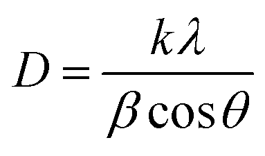
The SAED patterns (Fig. 3) of the sample CS5 containing 5 wt% of Cu2Se show rings corresponding to (103), (300), (310) and (323), and that of sample CS20 containing 20 wt% of Cu2Se show rings corresponding (103), (300), (310), (321) and (323) reflections of CdSe, respectively. The SAED pattern of the sample CS20 show ring corresponding to (640) reflection of Cu2Se indicating that the sample is nanocomposite. The spotty nature of the SAED pattern is an indication of the nanocrystalline nature of the samples.
 | ||
| Fig. 3 SAED patterns of nanocrystal thin films of CdSe:Cu2Se containing different concentrations of Cu2Se: (a) 5 wt%, (b) 20 wt%. | ||
X-ray photoelectron spectroscopy (XPS) measurements were carried out on CdSe:Cu2Se nanostructured film samples CS5 and CS20 containing 5 and 20 wt% Cu2Se to determine the valence states of the elements present in the samples. The XPS spectra of CS5 and CS20 in Fig. S3† show peaks corresponding to the elements C, Cd, Cu and Se elements. The C 1s peak located at 284.6 eV was taken as the internal standard for all the other elements and their peak positions were normalized with respect to the C 1s peak.40 The binding energies corresponding to the peaks Cd 3d5/2, Cd 3d3/2, Cu 2p3/2, and Se 3d5/2 obtained from the XPS spectra are 402.8, 411, 934 and 53.8 eV respectively.
The presence of doped Cu ions in samples CS5 and CS20 was investigated using narrow scan Cu 2p XPS data shown in Fig. 4. XPS plots of Cu 2p region show peaks at binding energies of 932.3 eV and 952.1 eV respectively corresponding to Cu 2p3/2 and Cu 2p1/2 for both the samples CS5 and CS20. The intensities of Cu 2p3/2 and the Cu 2p1/2 peaks increased as the Cu2Se wt% increased from 5% to 20%, but the peak positions did not change. The observed spin–orbit splitting was 19.8 eV which closely agreed with the reported value of 19.6 eV for Cu1+ oxidation state in Cu2Se nanoparticle.41,42 Satellite peaks at 940 and 945 eV of Cu2+ oxidation state reported in the literature were absent in the spectra of the samples CS5 and CS20.43–46 The absence of satellite peaks of Cu2+ ruled out the possibility for +2 oxidation state of Cu in the present samples.
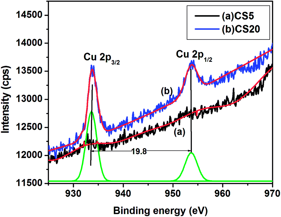 | ||
| Fig. 4 XPS plots of Cu 2p spectrum of CdSe:Cu2Se nanostructured thin films: (a) sample CS5, and (b) sample CS20. | ||
The AFM images of nanocrystal thin films of CdSe:Cu2Se containing different Cu2Se wt% of 5, 10, 20 and 30% are shown in Fig. 5. The AFM image of pure CdSe film is given as Fig. 1 in ref. 28. The surface morphology of the films was found to depend strongly on the Cu2Se wt%.
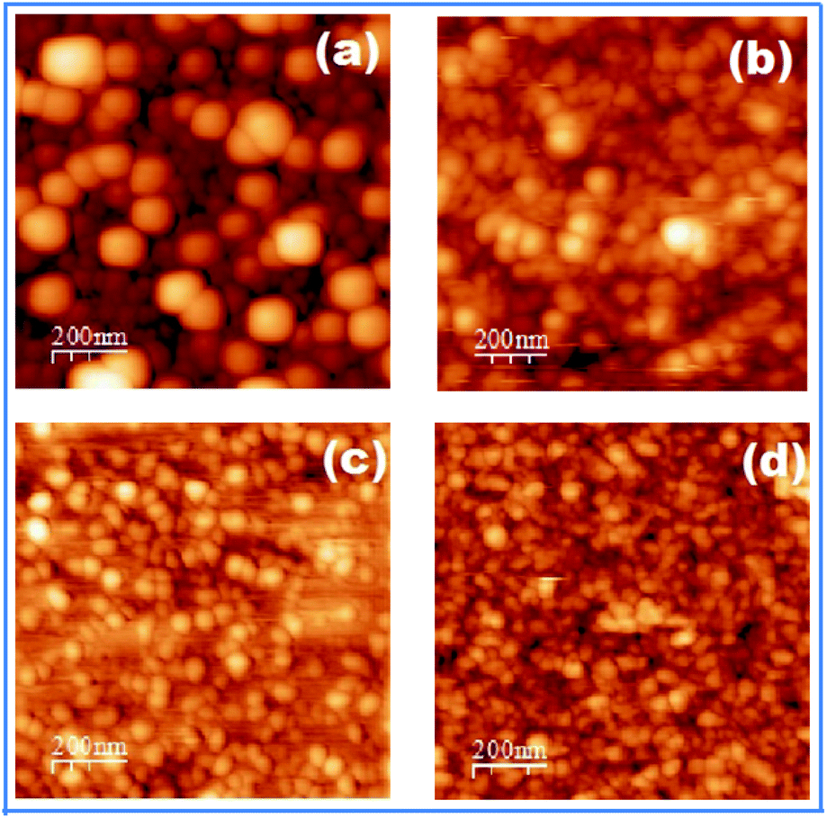 | ||
| Fig. 5 AFM images of nanocrystal thin films of CdSe:Cu2Se containing different concentrations of Cu2Se: (a) 5 wt%, (b) 10 wt%, (c) 20 wt% and (d) 30 wt%. | ||
The AFM images in Fig. 5 show that particles in each sample were of almost the same size and shape and the films exhibited a tendency to form uniformly sized and shaped particles for all concentration of Cu2Se. The particles in the AFM images showed a clear decrease in size with an increase in the Cu2Se wt%. The average sizes of the particles seen in the AFM images were measured to be 83, 76, 40 and 37 nm for the samples CS5, CS10, CS20 and CS30 respectively which were larger compared to the grain sizes obtained from XRD analysis (Table 1) using Scherrer equation leading to the inference that the grains in the nanocrystal thin films of CdSe:Cu2Se were aggregates of primary grain of size ∼33 to ∼26 nm (Table 1).
The optical transmission spectra of the nanocrystal thin films of CdSe:Cu2Se containing different Cu2Se wt% of 5, 10, 20 and 30 are shown in Fig. S4.† The optical transmission spectrum of pure CdSe film is given in Fig. 2(b) of ref. 28. The band gap energies of the film samples were determined from α2 versus hν plots (Tauc plot) shown in Fig. 6 where α is the optical absorption coefficient, h is the Planck's constant and ν is the light frequency. The Tauc plots of all the samples except that of CS5 gave two band gap energy values Eg1 and Eg2.47 The band gap values of the samples CS5, CS10, CS20 and CS30 are given in Table 1. Eg1 is close to the band gap of CdSe (1.74 eV), and it increases with increase in the wt% of Cu2Se in the thin film samples, while the value of Eg2 is close to the band gap of Cu2Se and it increases with increase in the wt% of Cu2Se. The existence of two band gaps for these samples containing higher wt% of Cu2Se indicated that these CdSe:Cu2Se samples were nanocomposites.
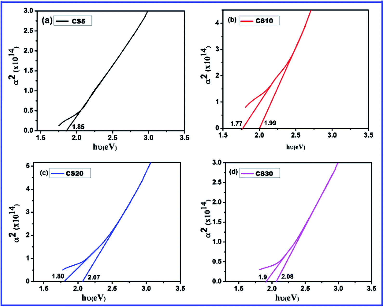 | ||
| Fig. 6 Plot of α2 against hν for nanocrystal thin films of CdSe:Cu2Se containing different concentrations of Cu2Se: (a) 5 wt%, (b) 10 wt%, (c) 20 wt% and (d) 30 wt%. | ||
Micro-Raman spectra of the nanocrystal thin films of pure CdSe, and of CdSe:Cu2Se samples containing different wt% of Cu2Se are shown in Fig. S5.† The spectrum of the sample CS5 shows a strong and broad peak centered at 206 cm−1 and a weak peak centered at 412 cm−1. The peak at 206 cm−1 was attributed to the longitudinal optical phonon (1LO), and the weak one at 412 cm−1 was attributed to the overtone (2LO) mode of CdSe. The very weak peak at 619 cm−1 was attributable to the 3LO mode. As the wt% of the Cu2Se increased, no considerable change was observed in the frequencies of the peaks. But, a weak peak was observed at 260 cm−1 in the spectrum of sample CS20 containing 20 wt% of Cu2Se which was attributed to Cu–Se vibration characteristic of binary copper selenides and which agreed well with the known Cu2Se Raman peak.48,49 With an increase in the wt% of Cu2Se from 20% to 30% the intensity of this peak increased very much.
Analysis of the intensities of the peaks in the spectra in Fig. 7 showed a variation in the intensity ratios of the LO overtone to the fundamental. The intensity ratio of the LO overtone to the fundamental can be used as a direct measure for the exciton–LO phonon coupling strength. Fig. 7 shows the variation of the intensity ratio of 2LO to 1LO modes of CdSe in nanocrystal thin films of CdSe:Cu2Se as a function of grain size. The intensity ratio I2LO/ILO for the films containing Cu2Se wt% of 5, 10, 20 and 30 were obtained as 0.32, 0.31, 0.3 and 0.29 respectively. For CdSe nanocrystals, Anne Myers Kelley reported values for 2LO/1LO ratio in the range of 0.2–0.5 implying a weaker electron–phonon coupling in nanoparticles than that in the bulk for which this ratio was reported to be greater than unity.50 Baranov et al.51 reported a value of ≈0.2 for electron–phonon coupling strength in colloidal core/shell CdSe/ZnS quantum dots which was in the same order of magnitude as previously reported for bare CdSe quantum dots.52,53 From Fig. 7 it can be observed that the intensity ratio of 2LO to LO decreased with the decrease in grain size. The electron–phonon coupling in nanoparticles is weakened with decrease in size due to the decrease in the density of states for both the electrons and the phonons, and also due to the increased overlap between the electron and the hole wave functions.54,55
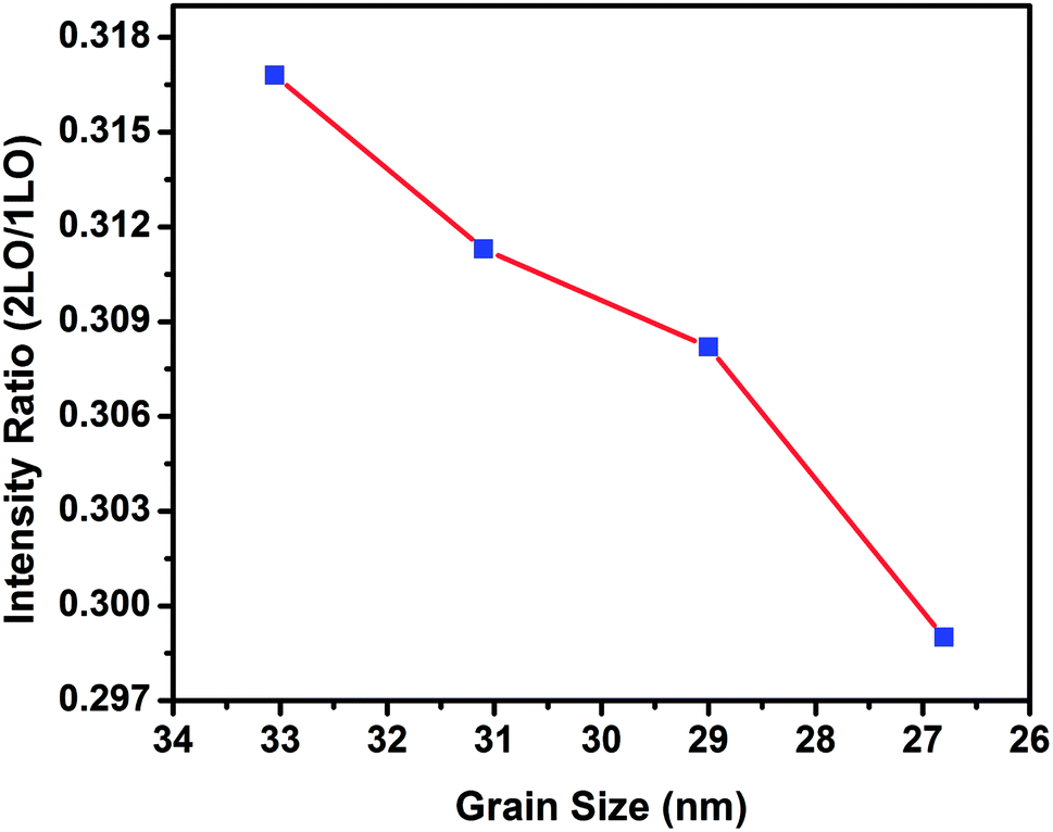 | ||
| Fig. 7 Variation of the intensity ratio of 2LO to LO Raman lines of nanocrystal thin films of CdSe:Cu2Se with grain sizes of CdSe. | ||
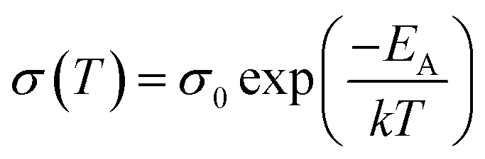
Fig. S6† shows the DC electrical conductivity (σ) of nanocrystal thin films of pure CdSe, and of CdSe:Cu2Se containing different wt% of Cu2Se. It was observed that the conductivity σ increased with increase in temperature, which confirmed the semiconducting nature of the nanostructured films. At room temperature, conductivity had the values 2.63 × 10⁻³, 1.12 × 10⁻², 1.94 × 10⁻² and 2.72 × 10⁻² Ω−1 cm−1 for the films containing Cu2Se wt% of 5, 10, 20 and 30 respectively. The conductivity of the samples was modelled based on the Arrhenius equation:
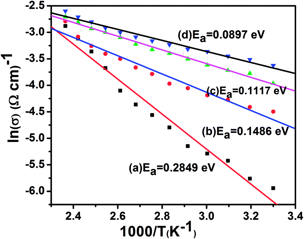 | ||
| Fig. 8 Arrhenius plot of nanocrystal thin films of CdSe:Cu2Se containing different concentrations of Cu2Se: (a) 5 wt%, (b) 10 wt%, (c) 20 wt% and (d) 30 wt%. | ||
Hall measurements could not be done on the CdSe:Cu2Se samples containing lower concentrations of Cu2Se since they were more resistive. Hall measurements carried at room temperature (308 K) and at 380 K were carried on the CdSe:Cu2Se film samples CS20 and CS30 containing Cu2Se concentrations of 20 and 30 wt% (Table 2). The positive Hall coefficient confirmed that both the film samples CS20 and CS30 were p-type semiconductors and that holes were the major charge carriers in these samples.56 The carrier mobility decreased and carrier concentration increased with increase in the Cu2Se wt% and with temperature.
| Sample code | CdSe:Cu2Se ratio in the samples |
Grain size (nm) | Temperature (K) | Carrier concentration (cm−3) | Hall coefficient RH (m3 C−1) | Mobility (μ) (×10−3) cm2 V−1 s−1 |
|---|---|---|---|---|---|---|
| CS20 | 80:20 |
29 | 308 | 0.13 × 10²⁰ | +4.81 × 10⁻⁷ | 9.15 |
| 380 | 0.08 × 10²¹ | +8.10 × 10⁻⁸ | 3.68 | |||
| CS30 | 70:30 |
26.8 | 308 | 0.39 × 10²⁰ | +1.58 × 10⁻⁷ | 4.21 |
| 380 | 0.18 × 10²¹ | +3.56 × 10⁻⁸ | 1.76 |
XRD and EDS results were utilized to determine the approximate value of x, where x is the at% of Cu2Se doped into CdSe. XRD patterns of the samples CS5 and CS10 in Fig. 1 did not show peaks of Cu2Se while the EDS analysis indicated the presence of respectively 3.87 and 9.24 at% of Cu (Table S1†) in these samples. Hence it was inferred that Cu2Se almost completely got substitutionally incorporated into the lattice of CdSe in the samples CS5 and CS10 and only a small percentage of Cu2Se below the level detectable through XRD remained in the samples as free Cu2Se. XRD patterns of the samples CS20 and CS30 showed the peaks of Cu2Se in addition to the peaks of CdSe. The at% of Cu2Se substitutionally incorporated into CdSe lattice in the samples CS20 and CS30 should be close to 10. Hence, we made the assumption that respectively 8 and 10 at% of Cu2Se got substitutionally incorporated into the CdSe lattice in the samples CS20 and CS30, and the remaining quantity existed as free Cu2Se nanograins in the samples. Hence the samples CS20 and CS30 actually consisted of nanograins of CdSe doped with Cu2Se (i.e., nanograins of Cd1−xCu2(x)Se where x is the at% of Cu2Se doped into CdSe. Cu2(x) means that for any value x, there be x Cu ions in the +1 oxidation state) and nanograins of Cu2Se. In the nanograins of Cd1−xCu2(x)Se, the concentration of Cu2Se was assumed to be more near the grain boundaries of these nanograins due to self purification mechanism.16,39 Hence CS20 and CS30 were considered as composites of nanograins of Cd1−xCu2(x)Se and Cu2Se, a model of which is shown in Fig. 9.
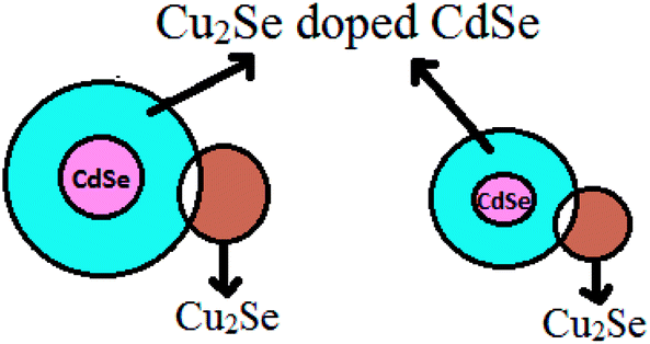 | ||
| Fig. 9 Model of the Cd1−xCu2(x)Se:Cu2Se nanocomposite. | ||
When a semiconductor heterojunction is formed between two dissimilar crystalline semiconductor materials with unequal band gaps, discontinuities between the valence band maxima or conduction band minima are produced at their interface. The discontinuities act as barriers to electrical transport across the interface.57,58 The semiconductor device performance mainly depends on the valence band offsets (ΔEV) and the conduction band offsets (ΔEC). For equilibrium at the junction, the Fermi levels of the two semiconductors must attain same energy by a transfer of an electron from the semiconductor 1 of higher Fermi level to the semiconductor 2 to lower Fermi level. This result in a partial depletion of the electrons near the junction in semiconductor 1 and therefore a bending upward of the band edges (Fig. 10(b)). There is also a corresponding redistribution of charge in semiconductor 2 and a bending downward of the band edges. This is the model developed by Anderson for current flow in p–n (n–p) semiconductor heterojunctions.59 Energy band diagram built using the Anderson model for semiconductor heterojunction between Cu2Se doped CdSe (i.e., Cd1−xCu2(x)Se) and Cu2Se in the present study is shown in Fig. 10(b). The band offsets of heterojunctions in an ideal case where no potential is created at the interface can be calculated using electron affinity model.58
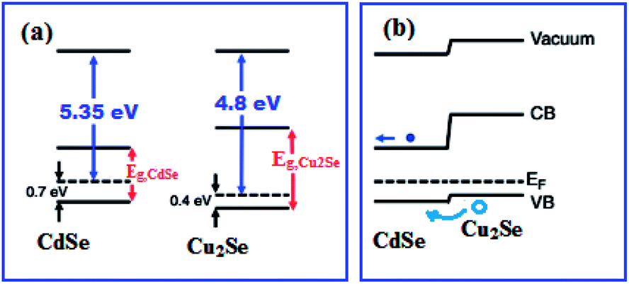 | ||
| Fig. 10 (a) Energy levels of the CdSe and Cu2Se, and (b) Anderson model energy band diagram of Cd1−xCu2(x)Se:Cu2Se heterojunction. | ||
The conduction band offset ΔEC for an electron at the heterojunction between Cd1−xCu2(x)Se and Cu2Se is
| ΔEC = χCd1−xCu2(x)Se − χCu2Se | (1) |
The valence band offset ΔEV for holes is
| ΔEV = (χCd1−xCu2(x)Se + Eg, Cd1−xCu2(x)Se) − (χCu2Se + Eg, Cu2Se) | (2) |
The electron affinity of Cd1−xCu2(x)Se determined using the equation,
| χCd1−xCu2(x)Se = ΦCd1−xCu2(x)Se − (Eg, Cd1−xCu2(x)Se − EF, Cd1−xCu2(x)Se) | (3) |
The electron affinity of Cd1−xCu2(x)Se is assumed to be linearly dependant on x and lie between 3.62 eV for nano CdSe determined using eqn (3) for x = 0 and 3.17 eV for nano Cu2Se determined using eqn (3) for x = 1.
Fig. 11 depicts the electron affinity of Cd1−xCu2(x)Se in the Cd1−xCu2(x)Se:Cu2Se nanocomposite as a function Cu at% x. The electron affinity χCd0.8Cu2(0.2)Se determined from the plot at x = 0.08 is 3.59 eV for the sample CS20. The value of Eg, Cd0.8Cu2(0.2)Se was taken as 1.80 eV (Table 1) and the value of Eg, Cu2Sewas taken as 2.07 eV (Table 1) for the sample CS20 to determine ΔEC and ΔEV. The electron affinity χCd0.7Cu2(0.3)Se determined from the plot at x = 0.1 is 3.56 eV for the sample CS30. The value of Eg, Cd0.7Cu2(0.3)Se was taken as 1.90 eV (Table 1) and the value of Eg, Cu2Sewas taken as 2.08 eV (Table 1) for the sample CS30 to determine ΔEC and ΔEV. The values of the ΔEC and ΔEV determined using the eqn (1) and (2) are respectively 0.46 eV and 0.19 eV for the sample CS20, and 0.44 eV and 0.26 eV for the sample CS30. The lower value of ΔEV created an easier pathway for hole movement from Cu2Se to CdSe. The applied voltage further reduced the valence band offset increasing the conductivity of the films.60 The hole density is larger for the sample CS30 than that for the sample CS20 leading to an increased hole current for the sample CS30.
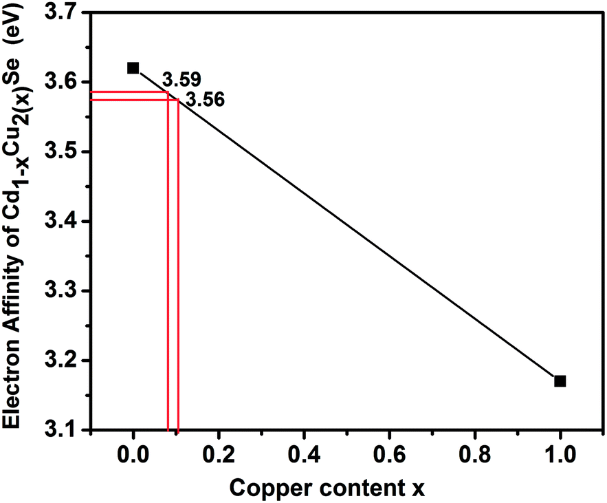 | ||
| Fig. 11 Plot of the electron affinity of Cd1−xCu2(x)Se vs. Cu at% (x) in Cd1−xCu2(x)Se:Cu2Se nanocomposite thin films. | ||
Literature reports show that the electrical transport properties in semiconductor heterojunctions are affected by the band offsets at the junction.57 Mews et al.61 fabricated an amorphous/crystalline silicon heterojunction with n-type crystalline silicon absorber and studied the hole transport with varying band offsets. Holes generated in the n-type crystalline silicon were directed towards the p–n junction and overcame the valence band offset (ΔEV) to enter the amorphous – SiOx:H and the amorphous – Si:H layer. They suggested that two possible transport paths existed for holes. First, the holes overcame the band offset barrier by thermionic emission. Second, they tunnelled into the amorphous – Si:H passivation layer and then travelled by tunnel hopping in its valence band tail states. Tunnel hopping was expected to become increasingly important for increased ΔEV.61 Alivov et al.62 reported the I–V characteristics of n-ZnO/p-AlGaN heterojunction light-emitting diodes on 6H–SiC substrates. They concluded from the study that the predominant device current was hole injection from the p-type Al0.12Ga0.88N into the n-type ZnO region of the heterojunction. Dogan et al.63 fabricated nanowire CdSe/Cu2Se heterojunctions by masking cation exchange via electron-beam irradiation. They performed electrical measurements on single CdSe nanowires before and after cation exchange and found that the partial conversion (CdSe → Cu2Se) of the nanowire between the two electrodes can enhance its dark and photoconductance by several orders of magnitude. The low valence band offset is responsible for the high conductivity in CdSe/Cu2Se heterojunctions.63 The explanation of easy hole transport leading to current in the present case of nanostructured CdSe:Cu2Se thin films are in agreement with the above interpretation of easy hole transport in the case of amorphous/crystalline silicon heterojunction, n-ZnO/p-AlGaN heterojunction and nanowire CdSe/Cu2Se heterojunction.
Current versus voltage (I–V) curves recorded for p–p heterojunctions formed between the CdSe:Cu2Se nanostructured films CS5, CS10, CS20 and CS30 deposited on ITO glass with similarly deposited Cu2Se film on ITO glass are shown in Fig. S7.† Current–voltage characteristic of pure CdSe film is given as Fig. S5 in ref. 28. The I–V curves are linear suggesting ohmic behaviour.
Fig. 12 shows I–V characteristics of the heterojunction formed by nanostructured CdSe:Cu2Se films CS5, CS10, CS20 and CS30 deposited on ITO coated glass with a similarly deposited ITO-CdSe film.64 The I–V characteristic for CS5 is liner showing ohmic behaviour of the junction, while that for CS10 indicates the behaviour of a p–n junction with a small knee voltage of 0.2 volts. The I–V characteristics of CS20 and CS30 are similar to that of a standard p–n junction diode. Although conduction starts from the lowest applied voltages, the knee voltage can be considered as ∼0.6 V and the forward resistance for both these samples is ∼100 Ω. This resistance is not high even though the contact between the two films at the junction may not be perfect and can be modulated by the sequential deposition of the two films on a single substrate, and such junctions may find practical applications such as photovoltaic (PV) solar cells and light-emitting diodes (LEDs).65,66 An ideal absorber for solar cells it should be preferably of p-type with a direct band gap of medium band gap energy with high optical absorption coefficient.67 The CdSe:Cu2Se nanocomposite films of the present study satisfy these conditions and hence may be used as absorber material in solar cells.
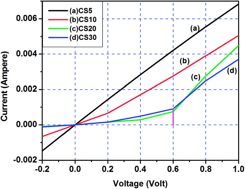 | ||
| Fig. 12 I–V characteristics of the heterojunction formed by nanostructured CdSe:Cu2Se films CS5, CS10, CS20 and CS30 deposited on ITO coated glass with a similarly deposited ITO-CdSe film. | ||
Conclusions
Nanocrystal thin films of CdSe:Cu2Se containing different wt% of Cu2Se were synthesized by a new technique of co-evaporation of CdSe and Cu2Se powder in nitrogen gas at a pressure larger than that required for conventional thin film deposition. The films consisted of nanograins of CdSe doped with Cu2Se for lower wt% of Cu2Se, and nanocomposites of Cd1−xCu2(x)Se and Cu2Se for higher wt% of Cu2Se. Energy band diagram built using the Anderson model was used for discussing the heterojunction characteristics of the junction between nanograins of Cd1−xCu2(x)Se and Cu2Se. To investigate the usefulness of the nanocrystal thin films of CdSe:Cu2Se for practical applications, the I–V characteristics of p–p and p–n heterojunctions formed by the films respectively with nanostructured films of similarly deposited Cu2Se and CdSe films were studied. The p–n heterojunctions studied may be useful for practical applications such as PV solar cells and LEDs.Conflicts of interest
There are no conflicts of interest to declare.Acknowledgements
The author M. A. K thanks the University Grants Commission for the award of an Emeritus Fellowship. The authors are thankful to UGC-DAE CSR, Indore, for providing facilities for micro-Raman, XPS and AFM measurements.References
- M. Shim and P. G. Sionnest, Nature, 2000, 407, 981–983 CrossRef PubMed.
- M. Mahima and R. Viswanatha, RSC Adv., 2018, 8, 22103–22112 RSC.
- A. Sahu, M. S. Kang, A. Kompch, C. Christian Notthoff, A. W. Wills, D. Deng, M. Winterer, C. D. Frisbie and D. J. Norris, Nano Lett., 2012, 12, 2587–2594 CrossRef.
- D. Mocatta, G. Cohen, J. Schattner, O. Millo, E. Rabani and U. Banin, Science, 2011, 332, 77–81 CrossRef PubMed.
- A. P. Litvin, I. V. Martynenko, F. P. Milton, A. V. Baranov, A. V. Fedorov and Y. K. Gun'ko, J. Mater. Chem. A, 2017, 5, 13252–13275 RSC.
- C. Ray and T. Pal, J. Mater. Chem. A, 2017, 5, 9465–9487 RSC.
- M. Karttunen, P. Ruuskanen, V. Pitkänen and W. M. Albers, J. Electron. Mater., 2008, 37, 951–954 CrossRef.
- P. Zukowski, T. N. Koltunowicz, O. Boiko, V. Bondariev, K. Czarnacka, J. A. Fedotova, A. K. Fedotov and I. A. Svito, Vacuum, 2015, 120, 37–43 CrossRef.
- M. Kumar, T. Kumar and D. K. Avasthi, Scr. Mater., 2015, 105, 46–49 CrossRef.
- Z. B. Sun, X. Z. Dong, W. Q. Chen, S. Nakanishi, X. M. Duan and S. Kawata, Adv. Mater., 2008, 20, 914–919 CrossRef.
- C. Dey, A. R. Molla, M. Goswami, G. P. Kothiyal and B. Karmakar, J. Opt. Soc. Am. B, 2014, 31, 1761–1770 CrossRef.
- W. Fan, Q. Zhang and Y. Wang, Phys. Chem. Chem. Phys., 2013, 15, 2632–2649 RSC.
- M. Nanu, J. Schoonman and A. Goossens, Adv. Funct. Mater., 2005, 15, 95–100 CrossRef.
- R. J. Beal, J. B. K. Kana and B. G. Potter Jr, Appl. Phys. Lett., 2012, 101, 031102 CrossRef.
- B. G. Potter, R. J. Beal and C. G. Allen, J. Appl. Phys., 2012, 111, 034305 CrossRef.
- S. Manu and M. A. Khadar, J. Mater. Chem. C, 2015, 3, 1846–1853 RSC.
- L. Maya, W. R. Allen, A. L. Glover and J. C. Mabon, J. Vac. Sci. Technol., B: Microelectron. Nanometer Struct.--Process., Meas., Phenom., 1995, 13, 361–365 CrossRef.
- T. Onishi, E. Iwamura, K. Takagi and K. Yoshikawa, J. Vac. Sci. Technol., A, 1995, 14, 2728–2735 CrossRef.
- W. Zhang, Z. Liu, Z. Liu and J. Zhao, Appl. Surf. Sci., 2012, 258, 6103–6106 CrossRef.
- A. Kongkanand, K. Tvrdy, K. Takechi, M. Kuno and P. V. Kamat, J. Am. Chem. Soc., 2008, 130, 4007–4015 CrossRef.
- W. C. Ching and Y. C. Fu, Nanoscale Res. Lett., 2013, 8, 33 CrossRef.
- S. Liu and X. Su, Anal. Methods, 2013, 5, 4541–4548 RSC.
- R. A. Andrievski and A. M. Gleze, Scr. Mater., 2001, 44, 1621–1624 CrossRef.
- B. Cantor and C. M. Allen, Scr. Mater., 2001, 44, 2055–2059 CrossRef.
- A. I. Gusev, Phys.-Usp., 1998, 41, 49–76 CrossRef.
- P. D. Persans, A. Tu, Y. J. Wu and M. Lewis, J. Opt. Soc. Am. B, 1989, 6, 818–823 CrossRef.
- A. I. Ekimov, F. Hache, M. C. S. Klein, D. Ricard and C. Flytzanis, J. Opt. Soc. Am. B, 1993, 10, 100–107 CrossRef.
- N. S. Babu and M. A. Khadar, Sol. Energy Mater. Sol. Cells, 2018, 178, 106–114 CrossRef.
- W. Zhang, C. Wang, L. Zhang, X. Zhang, X. Liu, K. Tang and Y. Qian, J. Solid State Chem., 2000, 151, 241–244 CrossRef.
- G. P. Sorokin, Y. M. Papshev and P. T. Oush, Sov. Phys. Solid State, 1966, 7, 1810–1811 Search PubMed.
- H. Okimura, T. Matsumae and R. Makabe, Thin Solid Films, 1980, 71, 53–59 CrossRef.
- Al-Mamun, A. B. M. O. Islam and A. H. Bhuiyan, J. Mater. Sci.: Mater. Electron., 2005, 16, 263–268 CrossRef CAS.
- A. M. Hermann and L. Fabick, J. Cryst. Growth, 1983, 61, 658–664 CrossRef CAS.
- N. J. Simi, R. Vinayakan and V. V. Ison, RSC Adv., 2019, 9, 15092–15098 RSC.
- X. Xu, J. Bullock, L. T. Schelhas, E. Z. Stutz, J. J. Fonseca, M. Hettick, V. L. Pool, K. F. Tai, M. F. Toney, X. Fang, A. Javey, L. H. Wong and J. W. Ager, Nano Lett., 2016, 16, 1925–1932 CrossRef CAS.
- S. Bhattacharyya and A. Gedanken, J. Phys. Chem. C, 2008, 112, 4517–4523 CrossRef CAS.
- A. Anu and M. A. Khadar, SN Appl. Sci., 2019, 1, 1057 CrossRef CAS.
- B. D. Cullity and S. R. Stock, Elements of X-ray Diffraction, Prentice Hall, New Jersey, 2001 Search PubMed.
- G. M. Dalpian and J. R. Chelikowsky, Phys. Rev. Lett., 2006, 96, 226802 CrossRef.
- N. Gleason, J. Guevremont and F. Zaera, J. Phys. Chem. B, 2003, 107, 11133–11141 CrossRef CAS.
- J. F. Moulder, W. F. Stickle, P. E. Sobol and K. D. Bomben, Handbook of X-ray Photoelectron Spectroscopy, Perkin-Elmer Corporation, Physical Electronics Division, Eden Prairie, 1995 Search PubMed.
- S. C. Riha, D. C. Johnson and A. L. Prieto, J. Am. Chem. Soc., 2011, 133, 1383–1390 CrossRef.
- C. Ge, L. Liu, X. Yao, C. Tang, F. Gao and L. Dong, Catal. Sci. Technol., 2013, 3, 1547–1557 RSC.
- L. Wang, J. R. Gaudet, W. Li and D. Weng, J. Catal., 2013, 306, 68–77 CrossRef.
- R. Zhang, D. Shi, Y. Zhao, B. Chen, J. Xue, X. Liang and Z. Lei, Catal. Today, 2011, 175, 26–33 CrossRef.
- L. Liu, Z. Yao, B. Liu and L. Dong, J. Catal., 2010, 275, 45–60 CrossRef.
- G. K. Larsen, B. C. Fitzmorris, C. Longo, J. Z. Zhang and Y. Zhao, J. Mater. Chem., 2012, 22, 14205–14218 RSC.
- V. I. Roca, A. P. Rodríguez, A. R. Rodríguez and J. R. Morante, J. Appl. Phys., 2007, 101, 103517 CrossRef.
- B. M. Sukarova, M. Najdoski, I. Grozdanov and C. J. Chunnilall, J. Mol. Struct., 1997, 410–411, 267–270 Search PubMed.
- A. M. Kelley, J. Phys. Chem. Lett., 2010, 1, 1296–1300 CrossRef CAS.
- A. V. Baranov, Y. P. Rakovich, J. F. Donegan, T. S. Perova, R. A. Moore, D. V. Talapin, A. L. Rogach, Y. Masumoto and I. Nabiev, Phys. Rev. B: Condens. Matter Mater. Phys., 2003, 68, 165306 CrossRef.
- M. C. Klein, F. Hache, D. Ricard and C. Flytzanis, Phys. Rev. B: Condens. Matter Mater. Phys., 1990, 42, 11123–11132 CrossRef CAS.
- C. Lin, K. Gong, D. F. Kelley and A. M. Kelley, ACS Nano, 2015, 9, 8131–8141 CrossRef CAS.
- M. Nirmal, C. B. Murray, D. J. Norris and M. G. Bawendi, ZPhys-e.D: At., Mol. Clusters, 1993, 26, 361–363 CAS.
- J. Z. Zhang, Acc. Chem. Res., 1997, 30, 423–429 CrossRef CAS.
- S. C. Riggs, R. D. McDonald, J. B. Kemper, Z. Stegen, G. S. Boebinger, F. F. Balakirev, Y. Kohama, A. Migliori, H. Chen, R. H. Liu and X. H. Chen, J. Phys.: Condens. Matter, 2009, 21, 412201 CrossRef.
- N. N. Halder, P. Biswas, B. Nagabhushan, S. Kundu, D. Biswas and P. Banerji, J. Appl. Phys., 2014, 115, 203719 CrossRef.
- B. Roul, M. Kumar, M. K. Rajpalke, T. N. Bhat and S. B. Krupanidhi, J. Phys. D: Appl. Phys., 2015, 48, 423001 CrossRef.
- A. G. Milnes and D. L. Feucht, Heterojunctions and Metal Semiconductor Junctions, Academic Press, New York, 1972 Search PubMed.
- R. Dalven, Introduction to Applied Solid State Physics, Springer Publication, Boston, 1990 Search PubMed.
- M. Mews, M. Liebhaber, B. Rech and L. Korte, Appl. Phys. Lett., 2015, 107, 013902 CrossRef.
- Y. I. Alivov, E. V. Kalinina, A. E. Cherenkov, D. C. Look, B. M. Ataev, A. K. Omaev, M. V. Chukichev and D. M. Bagnall, Appl. Phys. Lett., 2003, 83, 4719–4721 CrossRef CAS.
- S. Dogan, S. Kudera, Z. Dang, F. Palazon, U. Petralanda, S. Artyukhin, L. D. Trizio, L. Manna and R. Krahne, Nat. Commun., 2018, 9, 505 CrossRef.
- M. Zhou, H. Zhu, X. Wang, Y. Xu, Y. Tao, S. Hark, X. Xiao and Q. Li, Chem. Mater., 2010, 22, 64–69 CrossRef CAS.
- S. Menezes and A. Samantilleke, Sci. Rep., 2018, 8, 11350 CrossRef.
- R. Graft, T. Fischer, A. Gray and S. Kennerly, J. Appl. Phys., 1993, 74, 5705–5712 CrossRef CAS.
- S. R. Kodigala, Thin Films and Nanostructures, Elsevier, UK, 2010 Search PubMed.
Footnotes |
| † Electronic supplementary information (ESI) available. See DOI: 10.1039/c9ra10251e |
| ‡ Professor (Retired), Dept. of Physics & Former Honorary Director, Centre for Nanoscience and Nanotechnology, University of Kerala. |
| This journal is © The Royal Society of Chemistry 2020 |