
 Open Access Article
 This Open Access Article is licensed under a Creative Commons Attribution-Non Commercial 3.0 Unported Licence
Photocatalytic properties and energy band offset of a tungsten disulfide/graphitic carbon nitride van der Waals heterojunction
Jianjun Liu *ab and
Enda Huac
*ab and
Enda Huac
aSchool of Physics and Electronic Information, Huaibei Normal University, Huaibei, Anhui 235000, P. R. China. E-mail: jjliu@chnu.edu.cn
bKey Laboratory of Green and Precise Synthetic Chemistry and Applications, Ministry of Education, Huaibei, Anhui 235000, P. R. China
cSchool of Physical Sciences, University of Science and Technology of China, Hefei 230026, P. R. China
First published on 3rd February 2020
Abstract
Semiconductor heterojunctions have higher photocatalytic performance than a single photocatalytic material. However, the energy band offset and the photocatalytic reaction mechanism of these heterojunctions remain controversial. Here, tungsten disulfide (WS2)/graphitic carbon nitride (GCN) heterojunction photocatalytic water splitting is investigated with the hybrid density functional method. The band structures and the density of states (DOS) indicate that the WS2/GCN heterojunction is a type-II heterojunction, and its valence band offset and conduction band offset are 0.27 and 0.04 eV, respectively. The differential charge density distribution and the work function calculation indicate that a built-in electric field is formed in the WS2/GCN heterojunction. The potential of the built-in electric field is 0.16 V, and its direction is from the GCN surface to the WS2 surface. The built-in electric field separates the photogenerated electrons and the holes in space, effectively improving the photocatalytic efficiency of the WS2/GCN heterojunction. Our work provides insights into the electronic properties and the photocatalytic hydrogen evolution mechanism of the WS2/GCN heterojunction.
1. Introduction
Semiconductor photocatalytic materials can absorb solar energy for photocatalytic water splitting. This green technology is considered a promising solution for the current problems of environmental pollution and the energy crisis. TiO2 is the earliest material used for the photocatalytic water splitting into H2 and O2.1 However, TiO2 has a wide bandgap (3.2 eV), which indicates that it can only absorb ultraviolet light, and its solar light spectrum utilization rate is only approximately 4%. Searching for a new visible-light photocatalyst has subsequently become a popular topic in the field of solar energy. In recent years, with the discovery of graphene, a large number of two-dimensional semiconductor materials have been used for photocatalytic reactions. These materials have excellent physical properties. For example, graphitic carbon nitride (GCN) not only has a large specific surface area, but it also has a suitable conduction band potential and valence band potential.2 Transition metal disulfide, such as tungsten disulfide (WS2), has a narrow bandgap (approximately 1.8 to 2.1 eV) and high carrier mobility.3,4 These outstanding advantages enable the material to enhance its photocatalytic performance.5–7 However, a single two-dimensional semiconductor material cannot effectively overcome the recombination of photogenerated electrons and holes, and the resultant photocatalytic efficiency is relatively low.8 At present, an effective solution is to design a heterojunction to reduce the recombination rate of photogenerated carriers and improve the quantum efficiency of photocatalysts.9,10 A number of studies have reported that photocatalytic properties can be remarkably improved by constructing semiconductor heterostructures, such as phosphorene/g-C3N4,11 α-Fe2O3/g-C3N4,12 graphdiyne/g-C3N4,13 WO3/g-C3N4,14 MoS2/g-C3N4,15 g-C3N4/TiO2,16 ZnIn2S4/WS2,17 TiO2/WS2,18 etc. Recently, a semiconductor heterojunction constructed with WS2 and GCN is found to have excellent photocatalytic properties.19–25 Akple et al. prepared WS2/GCN composites and achieved enhanced photocatalytic activity for H2 production under visible light.19 Zhou et al. prepared an optimal WS2/GCN, with the highest photocatalytic hydrogen evolution at 154 μmol h−1 g−1, a value 34 times higher than that of GCN.20 WS2/GCN nano heterostructures are also widely studied through experiments, but their photocatalytic water splitting mechanisms remain to be contentious. Ma et al. investigated the electronic structures of triazine-based GCN/WS2 composites by performing first-principle calculations.26 However, in their experiment, the WS2/GCN nanocomposites appeared to have a heptazine-based GCN structure instead of a triazine-based GCN structure. Heptazine-based GCNs and triazine-based GCNs completely differ from each other in terms of crystalline and electronic structures. Thus far, no theoretical studies have been conducted on the heptazine-based WS2/GCN heterojunction photocatalytic mechanism. Therefore, the photocatalytic mechanism of the heptazine-based WS2/GCN heterojunction needs to be clarified through theoretical research. Building a reasonable heptazine-based WS2/GCN heterojunction and investigating its theoretical microscopic electronic structure to reveal the photocatalytic water splitting mechanism are highly desirable.In this study, we built heptazine-based WS2/GCN heterojunction and calculated its energy bands and density of states (DOS) by using the HSE06 hybrid density functional approach. The charge transfer of the WS2/GCN heterojunction was analyzed together with its work function and differential charge density. Then, the separation and mobility processes of the photogenerated electrons and the holes were investigated. A type II heterojunction photocatalytic water splitting mechanism was confirmed.
2. Computational methods
All calculations were performed with the Vienna ab initio simulation package (vasp).27 Exchange correction energy was described with the generalized gradient approximation (GGA) of the PBE functional method. The DFT-D3 method with Grimme correction was employed to describe the effect of the vdW interactions.28 The projector augmented wave method was adopted for the ion–electron forces. The energy cutoff was set to 520 eV, and the Monkhorst–Pack k-point mesh was set to 5 × 5 × 1. The structural optimizations converged when the energy and the forces reached 1.0 × 10⁻⁵ eV and 0.02 eV Å−1 on each atom, respectively. The screened hybrid HSE06 functional method was used to obtain the accurate energy band structures.3. Results and discussion
The 2D/2D WS2/GCN nano heterojunction is constructed using a monolayer GCN and a monolayer WS2. The heptazine-structured GCN is orthorhombic and belongs to the Cmc21 space group. The lattice constant (a = b = 7.14 Å) of the optimized monolayer GCN is extremely close to the experimental value.2,29 WS2 is the trigonal crystal and belongs to the P![[3 with combining macron]](https://www.rsc.org/images/entities/char_0033_0304.gif) m1 space group. The lattice constant (a = b = 3.18 Å) of the optimized monolayer WS2 only has a 0.95% error relative to the experimental value (3.15 Å).30 The monolayer g-C3N4 nanosheet of the
m1 space group. The lattice constant (a = b = 3.18 Å) of the optimized monolayer WS2 only has a 0.95% error relative to the experimental value (3.15 Å).30 The monolayer g-C3N4 nanosheet of the supercell is placed on the monolayer WS2 nanosheet of the 4 × 4 supercell as a means to build the WS2/GCN heterojunction (Fig. 1a–c). The lattice mismatch ratio between the optimized g-C3N4 supercell and the WS2 supercell is only 2.9%. The WS2/GCN heterojunction contains a total of 90 atoms, including 16 tungsten atoms, 32 sulfur atoms, 18 carbon atoms, and 24 hydrogen atoms. By calculating the minimum value of the energy of the single-layer GCN supercell and the single-layer WS2 supercell, the optimized lattice constant (12.54 Å) can be obtained. This value corresponds to the lattice constant of the 2D/2D WS2/GCN heterojunction. The vacuum layer thickness of the WS2/GCN heterojunction is set to 20 Å to eliminate the periodic influence of the contiguous layers. The calculated minimum distance between the two interfaces of the WS2/GCN heterojunction is 3.12 Å. The calculated distance between the two interfaces of the WS2/GCN heterojunction is extremely close to those of the other calculated GCN-based heterostructures.31–33
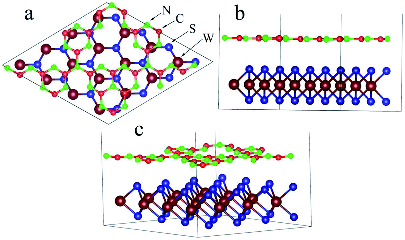 | ||
| Fig. 1 (a) Vertical view, (b) lateral view, and (c) three dimensional optimal WS2/GCN heterojunction. | ||
The C–N covalent bond lengths at the WS2/GCN heterojunction are approximately 1.35, 1.36, 1.41, and 1.50 Å, while the W–S covalent bond lengths are 2.40 and 2.41 Å. They hardly differ from the C–N covalent bond lengths (1.33, 1.39, and 1.48 Å) in the single-layer GCN nano-sheet and from the W–S covalent bond lengths (2.41 Å) in the single-layer WS2 nano-sheet. Therefore, the interaction is very weak between the GCN nano-sheet and the WS2 nano-sheet.
Interface formation energy is usually used to quantitatively describe the thermodynamic stability of formed heterostructures. The formulaic expression of the formation energy of the interface between GCN and WS2 is as follows:
| EF = EWS2/GCN − EWS2 − EGCN | (1) |
We first calculate the energy band structures of the single-layer GCN and the single-layer WS2 to further investigate the WS2/GCN heterojunction (Fig. 2a and b). The single-layer GCN is an indirect bandgap semiconductor with a valence band maximum (VBM) at the Γ high symmetry point and a conduction band minimum (CBM) at the M high symmetry point. The calculated indirect bandgap is 2.76 eV based on the HSE06 hybrid functional theory. The calculated result of the HSE06 hybrid functional theory is closer to the experimental value (2.7 eV) compared with that of the PBE functional method at 1.36 eV. The calculated monolayer WS2 is a direct bandgap semiconductor, and the CBM and the VBM are both located at the high symmetry point of K. The direct bandgap of the monolayer WS2 calculated by HSE06 hybrid functional approach is 2.28 eV, while the result calculated by the PBE functional approach is 1.59 eV. The bandgap of the monolayer WS2 measured experimentally is approximately 2.0 eV.35 The comparison indicates that the monolayer WS2 bandgap calculated by the HSE06 hybrid functional approach is closer to the experimental value and more precise than that calculated by the PBE functional.
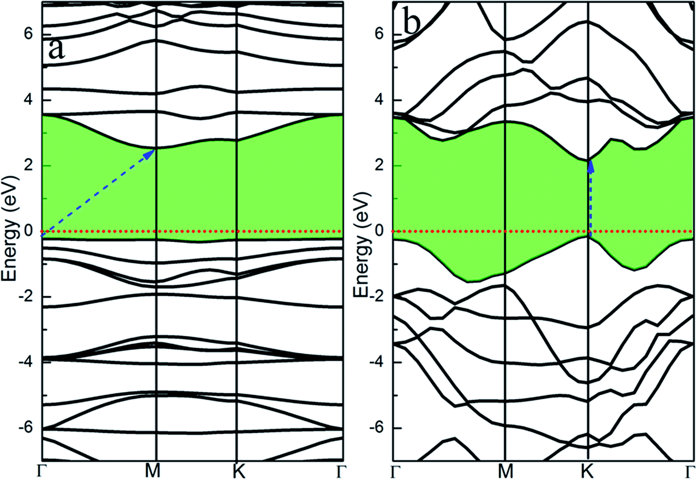 | ||
| Fig. 2 Energy band structures of monolayer (a) GCN and (b) WS2 nanosheet. | ||
The project energy band structure of the WS2/GCN heterojunction is calculated by the HSE06 hybrid functional approach (Fig. 3). The WS2/GCN heterojunction is a typical indirect bandgap semiconductor structure and its bandgap is 2.34 eV (Fig. 3a). The CBM of the heterojunction is located at the Γ point, by contrast, the VBM is not located at the high-symmetry point, and instead positioned between the high-symmetry points of M and K. Different from the energy band structures of the monolayer GCN and the monolayer WS2, the energy band structure of the WS2/GCN heterojunction is not just a simple addition of the energy band structures of GCN and WS2. The CBM and the VBM of the WS2/GCN heterojunction have both changed. At this point, the van der Waals interactions between the monolayer GCN and the WS2 nanosheet are affected by the energy band structure of the WS2/GCN heterojunction. In the conduction band region, the lowest energy orbitals of the conduction band belong to GCN, whereas the relatively high energy orbitals of the conduction band belong to WS2. The CBM of the WS2/GCN heterojunction is composed of the electron orbitals of GCN (Fig. 3b). In the valence band region, the highest energy orbitals of the conduction band are occupied by WS2, whereas the relatively low energy levels of the valence band are occupied by GCN. The VBM of the WS2/GCN heterojunction is composed of the electron orbitals of WS2 (Fig. 3c). The band edges of GCN and WS2 are shaped similar to a ladder, and the WS2/GCN heterojunction has a type II structure.
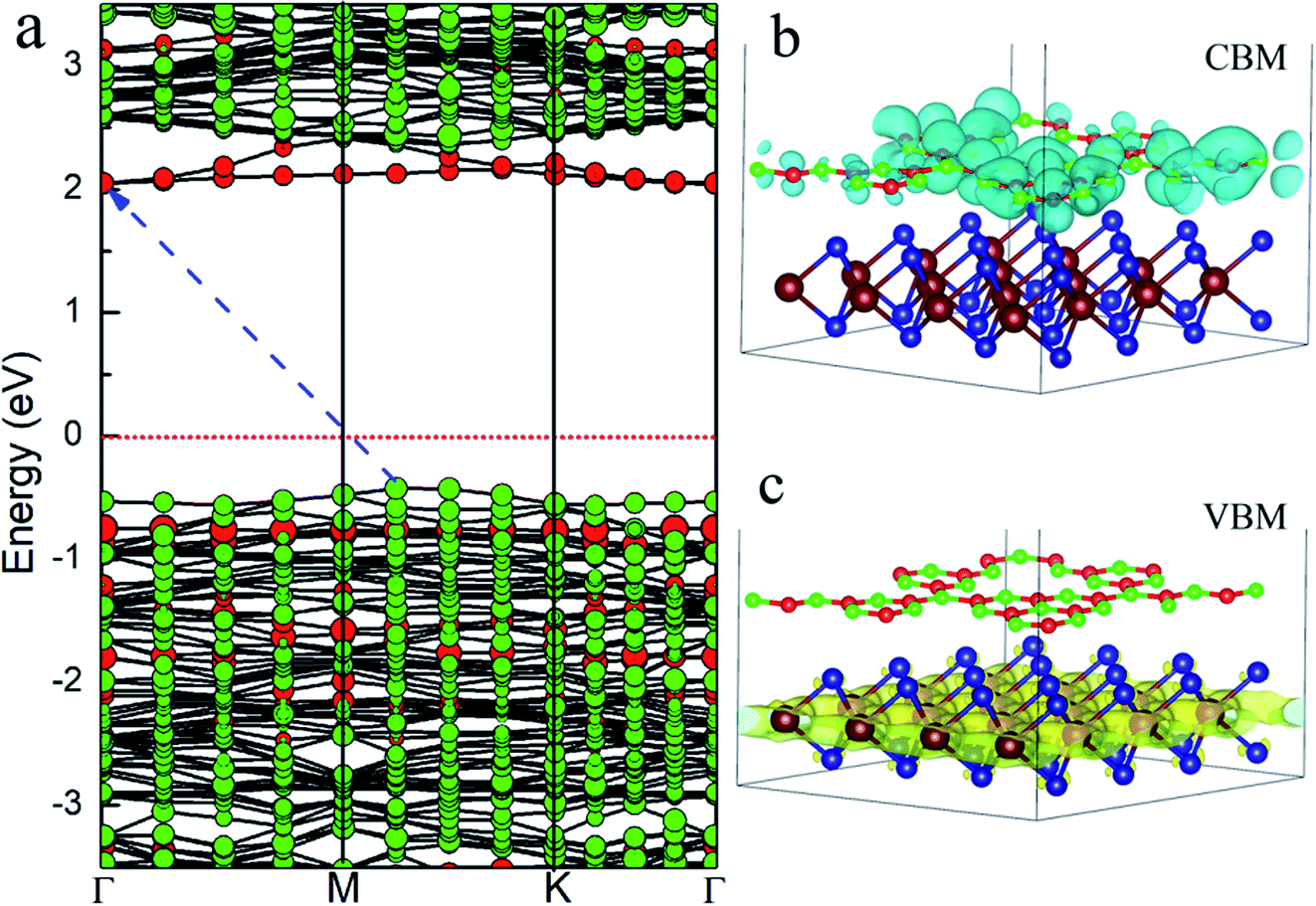 | ||
| Fig. 3 (a) The project energy band structure of WS2/GCN heterojunction; (b) the electron orbitals in the CBM and (c) VBM of WS2/GCN heterojunction. | ||
We calculated the total density of states (TDOS) and the partial density of states (PDOS) of WS2/GCN heterojunction by using HSE06 hybrid functional approach to further study the composition of the microelectronic structure. The VBM of the WS2/GCN heterojunction is mainly composed of W 5d and S 3p orbits, and also contains a small number of W 6s and W 5p orbits. The ratios were 77%, 19.5%, 1.7% and 1.5%, respectively. While the CBM of the WS2/GCN heterojunction is mainly occupied by C 2p and N 2p orbits, and also includes a small number of N 2s orbits. The ratios were 65.3%, 34.1% and 0.5%, respectively (Fig. 4). The configuration differs from the orbital composition of the monolayer GCN and the WS2 nanosheet. The van der Waals force between the GCN nanosheet and the WS2 nanosheet has changed the distribution of the electrons in the WS2/GCN heterojunction, and it has a type II heterostructure, which is consistent with the previous band structure's analytical results. The WS2/GCN heterojunction, as a type II structure, is conducive in promoting the separation of photoexcited electrons and holes, subsequently improving photocatalytic activity effectively.
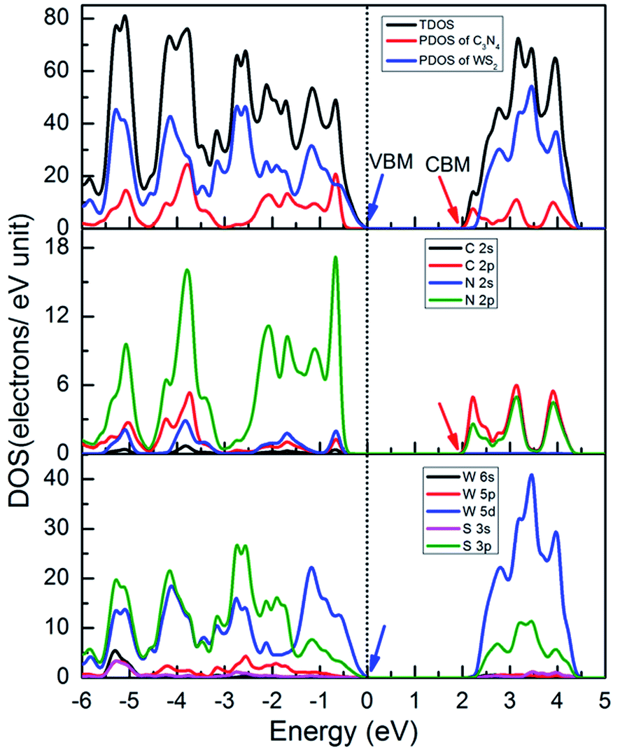 | ||
| Fig. 4 The TDOS and PDOS of WS2/GCN heterojunction. | ||
The interaction between the interfaces of the heterostructure will change the charge distribution on the two surfaces. Therefore, a built-in electric field will be formed within the heterostructure. This phenomenon can affect the transfer of photogenerated electrons and holes and further affect the photocatalytic performance of the heterojunction. Thus, an analysis of the charge distribution between the interfaces of the WS2/GCN heterojunction is extremely important.
First, we investigated the differential charge density distribution of the WS2/GCN heterojunction. The formula of the differential charge density is as follows:
| Δρ = ρWS2/GCN − ρGCN − ρWS2 | (2) |
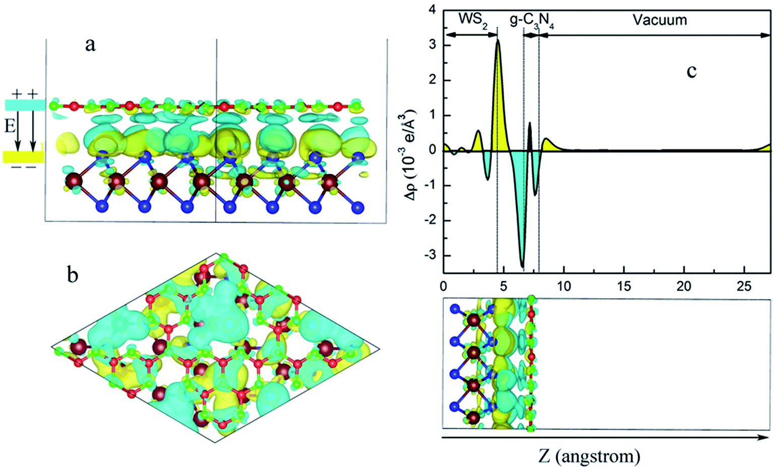 | ||
| Fig. 5 (a) The lateral view and (b) vertical view of the charge density difference of WS2/GCN heterojunction. (c) Electron density difference of plane projection along with Z axis for the WS2/GCN heterojunction. | ||
Second, we calculate the work functions of the monolayer WS2, the GCN nanosheet, and the WS2/GCN heterojunction to investigate the charge transfers between the WS2/GCN interface. The work function represents the minimum energy needed to lift an electron from the Fermi level to the vacuum. The formula of the work function is as follows:
| Φ = Evac − EFermi | (3) |
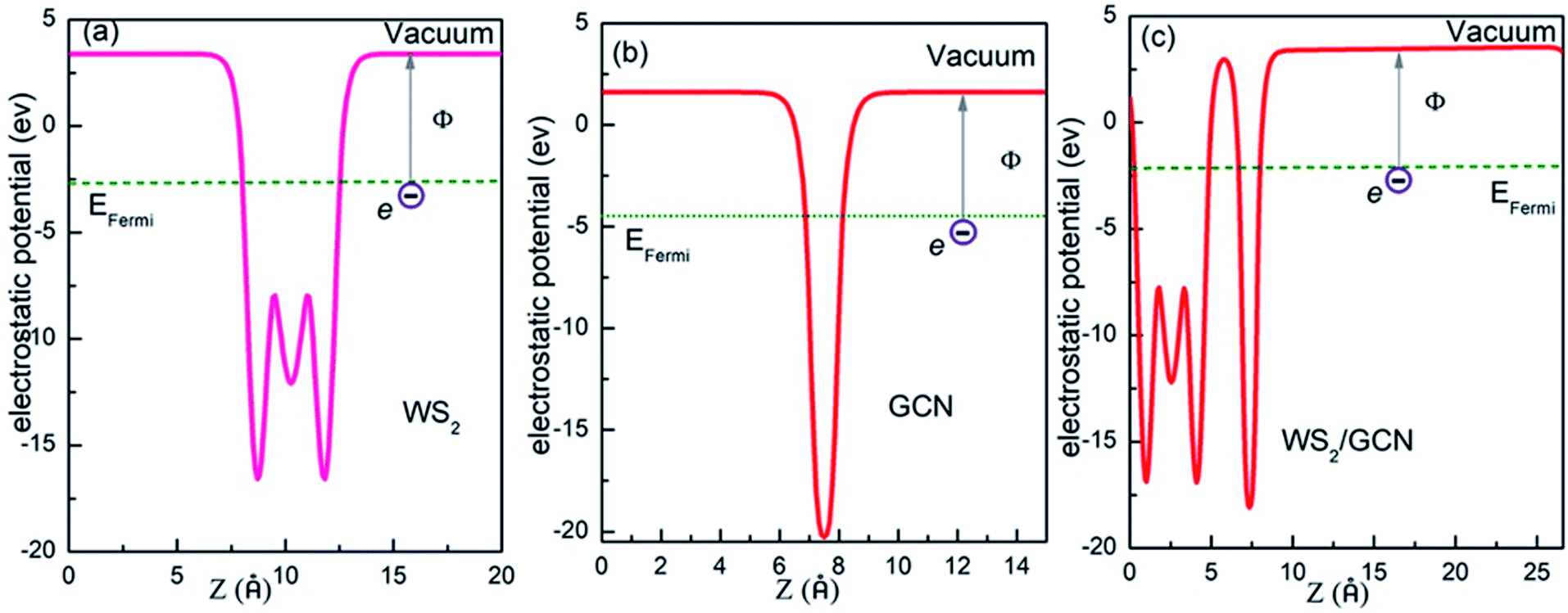 | ||
| Fig. 6 The electrostatic potential of (a) monolayer WS2, (b) GCN nanosheets and (c) WS2/GCN heterojunction. | ||
The VBM and CBM potentials of a semiconductor are the main factors of photocatalytic redox capacity. A positive VBM potential means strong oxidation capacity, while a negative CBM potential means strong reduction ability. Combined with the calculation for energy band structure, DOS, and electrostatic potential, we can further study the mechanism of the photocatalytic water splitting in the WS2/GCN heterojunction. According to the work function calculation, WS2 and GCN differ in their Fermi energy levels. When WS2 and GCN form a WS2/GCN heterojunction, the energy bands of the WS2 and the GCN will bend. The energy band of WS2 has a downward bending amount (qVD2) of 0.11 eV, the energy band of GCN has an upward bending amount (qVD1) of 0.06 eV, and the total band bending amount (qVD) is 0.16 eV, where VD is the potential of the built-in electric field between two interfaces of the WS2/GCN heterojunction. From the calculated results of the electrostatic potential and the DOS of the WS2/GCN heterojunction, we can derive the CBM and VBM potentials of the WS2/GCN heterojunction. The details are shown in Fig. 7. The CBM and VBM potentials of WS2 are −0.87 and 1.66 V (vs. NHE), respectively. Meanwhile, the CBM and VBM potentials of GCN are −0.67 V and 2.09 V, respectively. The conduction band offset (ΔEC) and the valence band offset (ΔEV) of the WS2/GCN heterojunction are 0.04 and 0.27 eV, respectively. When irradiated with light, the electrons on the valence bands of WS2 and GCN are excited to the conduction band. Meanwhile, the same number of holes are generated on the valence bands of WS2 and GCN. Driven by built-in electric field forces, the electrons on the conduction bands of WS2 transfer to the conduction bands of GCN, while the holes on the valence bands of GCN transfer to the valence bands of WS2. Consequently, the photoexcited electrons and holes gather in the conduction bands of GCN and the valence bands of WS2, respectively. These phenomena result in the separation of photoexcited electrons and holes in space, effectively avoiding a large number of recombination of photoexcited electrons and holes, and they extend the lifetime of the photoexcited carriers. Therefore, the photogenerated electrons and the holes can further increase the probability of surface photocatalytic reaction, effectively improving the photocatalytic efficiency of the WS2/GCN heterojunction. The photoexcited electrons' potential in the CBM of GCN is −0.67 V, which is negative relative to the reduction potential of H+/H2 (0 V), indicating sufficient ability to reduce hydrogen ion to hydrogen. Meanwhile, the photogenerated holes' potential in the VBM of WS2 is 1.66 V, which is more positive than the potential of O2/H2O (1.23 V), suggesting sufficient ability to oxidize water to oxygen. The results of the theoretical analysis are consistent with the experimental study. In summary, the WS2/GCN heterojunction has a type II photocatalytic structure with staggered energy levels. This configuration can effectively promote the separation of photogenerated electrons and holes in space, and it has enough potential to decompose water to produce hydrogen and oxygen.
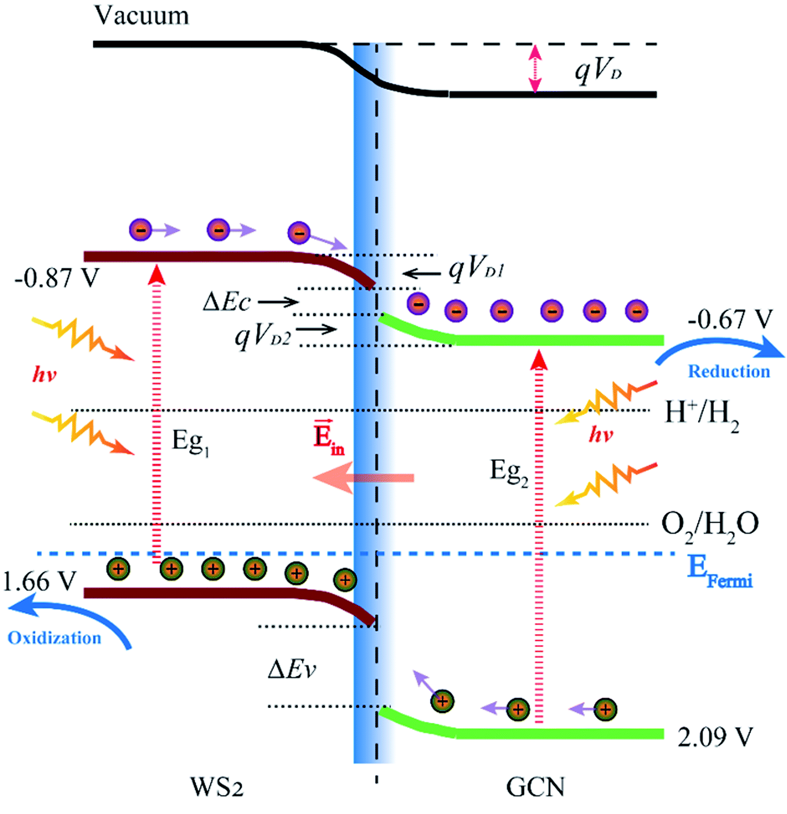 | ||
| Fig. 7 Photocatalytic mechanism of type II WS2/GCN heterojunction. | ||
4. Conclusion
In this work, the electronic structures and the photocatalytic water decomposition of the WS2/GCN heterojunction are systematically investigated by using the hybrid density functional approach. The bandgap of the monolayered WS2, the GCN nanosheet and the WS2/GCN heterojunction are 2.28, 2.76, and 2.34 eV, respectively. The calculated interfacial formation energy and the interface distance indicate that the interface interaction of the WS2/GCN heterojunction belong to a van der Waals force. Furthermore, the WS2/GCN heterojunction has a typical van der Waals heterostructure. The energy band structures and the DOS calculations reveal that the WS2/GCN heterojunction has a typical type-II heterostructure, and its valence band offset and conduction band offset are 0.27 and 0.04 eV, respectively. The different Fermi energy levels of the monolayer WS2 and the GCN nanosheet causes the energy band to bend at the interface when they form a heterojunction. The total band bending amount (qVD) is 0.16 eV, and the potential of the built-in electric field between the interfaces of the WS2/GCN heterojunction is 0.16 V. The built-in electric field can promote the separation of the photoexcited electrons and the holes in space, and a large number of recombination of photoexcited electrons and holes can be effectively avoided. Therefore, photogenerated electrons and holes can further increase the probability of surface photocatalytic reaction, effectively improving the photocatalytic efficiency of the WS2/GCN heterojunction. In terms of WS2/GCN heterojunction photocatalytic water decomposition, the photoexcited electrons' potential in the CBM of GCN is −0.67 V, which is negative relative to the reduction potential of H+/H2 (0 V), indicating sufficient ability to reduce hydrogen ion to hydrogen. Meanwhile, the photogenerated holes' potential in the VBM of WS2 is 1.66 V, which is more positive than the potential of O2/H2O (1.23 V), suggesting sufficient the ability to oxidize water to oxygen. Our work not only elucidates the photocatalytic water decomposition mechanism of the WS2/GCN heterostructure but also provides a good idea for designing photocatalytic heterojunctions.Conflicts of interest
There are no conflicts to declare.Acknowledgements
This work was supported by Anhui Provincial Natural Science Foundation (No. 1908085MA23 and 1908085QE222) and Natural Science Foundation of Education Department of Anhui Province (No. KJ2017A385)Notes and references
- A. Fujishima and K. Honda, Nature, 1972, 238, 37–38 CrossRef CAS PubMed.
- X. Wang, K. Maeda, A. Thomas, K. Takanabe, G. Xin, J. M. Carlsson, K. Domen and M. Antonietti, Nat. Mater., 2009, 8, 76–80 CrossRef CAS PubMed.
- Y. Sang, Z. Zhao, M. Zhao, P. Hao, Y. Leng and H. Liu, Adv. Mater., 2015, 27, 363–369 CrossRef CAS PubMed.
- V. Q. Bui, T. T. Pham, D. A. Le, C. M. Thi and H. M. Le, J. Phys.: Condens. Matter, 2015, 27, 305005 CrossRef PubMed.
- B. Mahler, V. Hoepfner, K. Liao and G. A. Ozin, J. Am. Chem. Soc., 2014, 136, 14121–14127 CrossRef CAS PubMed.
- C. Tan, X. Cao, X. J. Wu, Q. He, J. Yang, X. Zhang, J. Chen, W. Zhao, S. Han, G. H. Nam, M. Sindoro and H. Zhang, Chem. Rev., 2017, 117, 6225–6331 CrossRef CAS PubMed.
- H. Huang, K. Xiao, N. Tian, F. Dong, T. Zhang, X. Du and Y. Zhang, J. Mater. Chem. A, 2017, 5, 17452–17463 RSC.
- M. Yousefi, M. Faraji, R. Asgari and A. Z. Moshfegh, Phys. Rev. B, 2018, 97, 195428 CrossRef CAS.
- T. Su, Q. Shao, Z. Qin, Z. Guo and Z. Wu, ACS Catal., 2018, 8, 2253–2276 CrossRef CAS.
- N. Tian, H. Huang, X. Du, F. Dong and Y. Zhang, J. Mater. Chem. A, 2019, 7, 11584–11612 RSC.
- J. R. Ran, W. W. Guo, H. L. Wang, B. C. Zhu, J. G. Yu and S. Z. Qiao, Adv. Mater., 2018, 30, 6 Search PubMed.
- X. J. She, J. J. Wu, H. Xu, J. Zhong, Y. Wang, Y. H. Song, K. Q. Nie, Y. Liu, Y. C. Yang, M. T. F. Rodrigues, R. Vajtai, J. Lou, D. L. Du, H. M. Li and P. M. Ajayan, Adv. Energy Mater., 2017, 7, 7 Search PubMed.
- Q. L. Xu, B. C. Zhu, B. Cheng, J. G. Yu, M. H. Zhou and W. K. Ho, Appl. Catal., B, 2019, 255, 10 CrossRef.
- J. W. Fu, Q. L. Xu, J. X. Low, C. J. Jiang and J. G. Yu, Appl. Catal., B, 2019, 243, 556–565 CrossRef CAS.
- Y. J. Yuan, Z. K. Shen, S. T. Wu, Y. B. Su, L. Pei, Z. G. Ji, M. Y. Ding, W. F. Bai, Y. F. Chen, Z. T. Yu and Z. G. Zou, Appl. Catal., B, 2019, 246, 120–128 CrossRef CAS.
- J. G. Yu, S. H. Wang, J. X. Low and W. Xiao, Phys. Chem. Chem. Phys., 2013, 15, 16883–16890 RSC.
- W. Pudkon, S. Kaowphong, S. Pattisson, P. J. Miedziak, H. Bahruji, T. E. Davies, D. J. Morgan and G. J. Hutchings, Catal. Sci. Technol., 2019, 9, 5698–5711 RSC.
- Y. C. Wu, Z. M. Liu, Y. R. Li, J. T. Chen, X. X. Zhu and P. Na, Chin. J. Catal., 2019, 40, 60–69 CrossRef CAS.
- M. S. Akple, J. X. Low, S. Wageh, A. A. Al-Ghamdi, J. G. Yu and J. Zhang, Appl. Surf. Sci., 2015, 358, 196–203 CrossRef CAS.
- Y. L. Zhou, X. Y. Ye and D. Y. Lin, Int. J. Hydrogen Energy, 2019, 44, 14927–14937 CrossRef CAS.
- M. M. Shao, W. Z. Chen, S. J. Ding, K. H. Lo, X. W. Zhong, L. M. Yao, W. F. Ip, B. M. Xu, X. S. Wang and H. Pan, ChemSusChem, 2019, 12, 3355–3362 CrossRef CAS PubMed.
- P. Zeng, X. Y. Ji, Z. G. Su and S. P. Zhang, RSC Adv., 2018, 8, 20557–20567 RSC.
- Y. N. Ma, J. Li, E. Z. Liu, J. Wan, X. Y. Hu and J. Fan, Appl. Catal., B, 2017, 219, 467–478 CrossRef CAS.
- H. H. Tran, D. H. Truong, T. T. Truong, T. Xuan Dieu Nguyen, Y.-S. Jin, S. J. Kim and V. Vo, Bull. Korean Chem. Soc., 2018, 39, 965–971 CrossRef CAS.
- J. Huang, J. Mei, J. Han, H. Liang, W. Wang, B. Dong and L. Cao, J. Colloid Interface Sci., 2019, 556, 224–231 CrossRef CAS PubMed.
- X. G. Ma, C. Chen, J. S. Hu, M. K. Zheng, H. H. Wang, S. J. Dong, C. Y. Huang and X. B. Chen, J. Alloys Compd., 2019, 788, 1–9 CrossRef CAS.
- G. Kresse and J. Furthmüller, Phys. Rev. B: Condens. Matter Mater. Phys., 1996, 54, 11169–11186 CrossRef CAS PubMed.
- S. Grimme, J. Comput. Chem., 2006, 27, 1787–1799 CrossRef CAS PubMed.
- J. Gracia and P. Kroll, J. Mater. Chem., 2009, 19, 3013–3019 RSC.
- W. J. Schutte, J. L. De Boer and F. Jellinek, J. Solid State Chem., 1987, 70, 207–209 CrossRef CAS.
- J. Wang, Z. Guan, J. Huang, Q. Li and J. Yang, J. Mater. Chem. A, 2014, 2, 7960–7966 RSC.
- J. Zhang, F. Ren, M. Deng and Y. Wang, Phys. Chem. Chem. Phys., 2015, 17, 10218–10226 RSC.
- J. Liu, J. Phys. Chem. C, 2015, 119, 28417–28423 CrossRef CAS.
- T. Björkman, A. Gulans, A. V. Krasheninnikov and R. M. Nieminen, Phys. Rev. Lett., 2012, 108, 235502 CrossRef PubMed.
- Y. Sun, H. Cheng, S. Gao, Z. Sun, Q. Liu, Q. Liu, F. Lei, T. Yao, J. He, S. Wei and Y. Xie, Angew. Chem., Int. Ed., 2012, 51, 8727–8731 CrossRef CAS PubMed.
| This journal is © The Royal Society of Chemistry 2020 |