
 Open Access Article
 This Open Access Article is licensed under a Creative Commons Attribution-Non Commercial 3.0 Unported Licence
Tunable spin-polarized band gap in Si2/NiI2 vdW heterostructure†
Douglas Duarte de Vargas* and
Rogério José Baierle
Departamento de Física, Universidade Federal de Santa Maria, Av. Roraima, 1000, Santa Maria, RS, Brazil. E-mail: duartedevargas@gmail.com
First published on 2nd March 2020
Abstract
Using density functional theory (DFT) calculations we investigate the structural and electronic properties of a heterogeneous van der Waals (vdW) structure consisting of silicene and NiI2 single layers. We observe an interaction between the two layers with a net charge transfer from the ferromagnetic semiconductor NiI2 to silicene, breaking the inversion symmetry of the silicene structure. However, the charges flow in opposite directions for the two spin channels, which leads to a vdW heterostructure with a spin-polarized band gap between the π and π* states. The band gap can be tuned by controlling the vertical distance between the layers. The features shown by this vdW heterostructure are new, and we believe that silicene on a NiI2 layer can be used to construct heterostructures which have appropriate properties to be used in nanodevices where control of the spin-dependent carrier mobility is necessary and can be incorporated into silicon based electronics.
1 Introduction
In 2004, K. Novoselov and A. Geim isolated a single layer of C atoms from graphite through the mechanical exfoliation technique with scotch adhesive tape1 and obtained graphene, which was the first stable two dimensional (2D) material. In the 2D structure, the C atoms are arranged in a honeycomb lattice and bond with three other C atoms, forming σ bonds, which give graphene exceptional mechanical and elastic properties. The electrons from the perpendicular orbital (pz) make weak π-bonds and determine the electronic properties. The properties of graphene, like extraordinary thermal and electronic conductivity, quasirelativistic massless Dirac fermions, and the quantum spin Hall effect (QSHE),2 have prompted interest in synthesizing other 2D materials. Considering that Si is isovalent to C and Si is the main semiconductor material used in electronic devices, a stable structure of Si in the 2D configuration is quite important for nanodevices.The Si counterpart of graphene is silicene, which has been successfully synthesized on Ag and ZrB2 surfaces.3–5 Molecular dynamics (MD) shows that silicene can be grown through island migration and coalescence on Ir(III) surfaces.6 Silicene presents a buckled structure7 which does not change the inversion symmetry of the sublattices, and silicene has many of the non-conventional properties exhibited by graphene, in particular the quasirelativistic massless Dirac fermions and QSHE. The spin–orbit coupling (SOC) in silicene is larger than in graphene, causing the massless Dirac fermions in silicene to behave in an atypical way when subjected to an external magnetic field, and new QSHE phenomena can be anticipated in the experimentally accessible temperature regime.8,9 For silicon nanoribbons (SiNRs), high magnetoresistance (MR) is predicted by first principles quantum transport calculations,10 and silicene on MgX (X = Cl, Br, and I) is predicted to be a promising electronic material for Li-ion batteries.11
Despite these interesting electronic properties, silicene (similar to graphene) lacks a finite band gap, which is crucial for electronic applications in semiconductor technology where control of the electric current is necessary. Moreover, for spintronics applications, it is required that the two spin channels present different behavior when subjected to an external electromagnetic field. To achieve the opening of the band gap, external electric fields,12,13 the adsorption of atoms,14,15 and small strain engineering16,17 have been studied. Metallic substrates can interact with silicene, breaking the inversion symmetry and leading to a small band gap between the π and π* states,18–22 however a strong interaction with the substrate can damage the linear dispersion of the π and π* states.4 So, it is necessary to find a substrate in which the interactions occur via van der Waals (vdW) forces. It can be obtained by integrating silicene with other 2D materials.21,23–26 The role of the substrate is to create a tunable band gap but without damaging the linear dispersion of the π and π* states. Such heterostructures formed by integrating two different materials present a large spectrum of applications as shown in recent papers.27,28
Recently, single layered metal dihalides have been shown to be energetically stable and to exhibit intrinsic ferromagnetism (FM).29,30 Bulk metal dihalides have a natural layered structure and theoretical investigations show that layers can potentially be extracted using exfoliation techniques.31,32 Nickel iodide (NiI2) consists of strongly bonded triple ions (I−, Ni2+ and I−) in a hexagonal lattice with a trigonal structure. The layers weakly interact with each other via cohesive forces (vdW interactions). In summary, NiI2 presents very interesting properties not observed in most studied homogeneous 2D materials.
Therefore, due to their similar honeycomb structures, the integration of silicene and NiI2 layers into vertical vdW heterostructures is a feasible strategy to investigate the interfacial coupling and spin-polarized properties. By means of first principles calculations based on density functional theory (DFT), we study the structural and electronic properties of a vdW heterostructure formed from silicene and the FM semiconductor NiI2. We observe that, due to the interactions and the inhomogeneous spin-polarized charge distribution of NiI2, there is spin-polarized charge transfer between layers and the inversion symmetry of silicene is broken. As a consequence, the majority and minority spin carriers show different electronic properties, causing the vdW heterostructure to exhibit a small band gap for each spin channel, which can be controlled by adjusting the vertical distance between the layers. This finding shows the possibility of using NiI2 integrated with silicene in a vdW heterostructure for spintronics devices.
2 Calculation procedure
The structural and electronic properties of the layer materials are obtained using first principles calculations within spin-polarized density functional theory (SP-DFT)33,34 as implemented in the Quantum Espresso (QE) code.35,36 For single layers, the exchange–correlation functional (εxc) is modulated through the generalized gradient approximation (GGA) in the Perdew–Burke–Ernzerhof (PBE) form.37 To obtain the ground states of single layers, SOC was added to the calculations. It is well known that the local and semi-local approximations for εxc are not able to describe long range vdW interactions. So, to calculate the geometric configuration, binding energy and electronic properties of the bilayer system (silicene/NiI2), the vdW-DF2 functional38 with the c09 exchange correction39 has been used. Additional calculations have been performed using the DFT+U scheme. In this scheme, two terms (U and J) are used to correct the problem when a local (LDA) or semi-local (GGA) approximation is used for the εxc functional. The on-site Coulomb term U and the site exchange term J come from the Hubbard model, and different values of U and J are checked for a better description of strongly correlated electronic states (d and f orbitals). In our calculations, different values of U and J parameters were used to describe the d electrons of the Ni atom.The strong interaction between the valence electrons and the atomic core is modulated by ultrasoft pseudopotentials.40 The single and bilayer structures are arranged in the X–Y plane within the hexagonal honeycomb structure and planar periodic conditions. The Brillouin Zone (BZ) is sampled by special  obtained using the Monkhorst–Pack41 scheme with an uniform grid of 14 × 14 × 1 centered at the Γ-point. To avoid any artificial interaction between periodic images perpendicular to the X–Y plane, a vacuum region of approximately 17 Å (20 Å) is used along the Z direction for the bilayer (single layer). Plane waves (PWs) with energy cutoff of 70 Ry (≈950 eV) are employed as basis sets to expand the one electron wave function (Kohn–Sham orbitals). These basis set functions were chosen to guarantee convergence of the total energy per atom of the pristine system (single layer system) to within 10−6 eV. The geometric structures are fully relaxed until the residual Hellmann–Feynman forces are less than 0.01 eV Å−1.
3 Results and discussion
3.1 Geometric structure and electronic properties of NiI2 monolayer and silicene
Using the methodology described in the previous section and the basic unit cell (3 atoms), we obtain 3.944 Å for the equilibrium lattice parameter of the NiI2 single layer in the 2D hexagonal structure. The Ni–I bond length is 2.748 Å, and the thickness of the NiI2 monolayer (the vertical distance between I atoms) is 3.020 Å. These values are in good agreement with previous calculations.29,30,32The magnetic structure of the bulk NiI2 was determined by neutron diffraction, with spins ordered ferromagnetically in each Ni2+ ion and a magnetic moment of 1.6 μB (ref. 42), and for a single layer the calculated magnetic moment is 2 μB.43 In our calculations, the magnetic ordering of the NiI2 single layer is determined by increasing the size of the unit cell (supercell with 12 atoms). The ferromagnetic (FM) or antiferromagnetic (AFM) spin ordering is settled, and the exchange energy (EEX = EAFM − EFM) is calculated. We found that NiI2 is more stable (ground state) with FM coupling with a exchange energy of 38.775 meV per Ni atom. The spin-polarized calculations demonstrate that NiI2 possesses a magnetic moment of 2 μB per unit cell, in good agreement with the magnetic moment of the free Ni atom described by Hund’s rules. The main contribution to the magnetic moment of the NiI2 single layer comes from the Ni atoms (≈1.533 μB), while each I atom contributes approximately 0.233 μB to the magnetic moment. The high magnetic moment of NiI2 enables us to study the effects of a magnetic material interacting with silicene. The use of different values of U and J does not change the magnetic moment of the NiI2 single layer.
For FM systems, the Curie temperature (TC) is one of the critical properties. The methods to estimate TC include mean-field theory and statistical Monte Carlo simulations. However, considering a set of Ising magnetic spins located at sites on a triangular lattice of 2D nickel, TC has an analytical form44 given by
 | (1) |
 | (2) |
In eqn (2), EEX is the exchange energy per nickel atom, z is the number of nearest neighbours (z = 6 for a triangular lattice) and S is the total spin of each nickel atom (S = 1 for nickel in an octahedral configuration). From our analytical calculations, TC is found to be 136.52 K, which is close to the value obtained from Monte Carlo simulations.30,32
For the NiI2 bulk system, the electronic band structure calculation yielded fully occupied 5p-iodine and partially filled 3d-nickel sub-bands,45 with the system being a Mott insulator.46 This was confirmed by photoconductivity measurements showing an indirect transition and an energy band gap of 1.8 eV.47 The calculated electronic band structure shows that the NiI2 single layer is an indirect band gap semiconductor for both spin channels (see Fig. 1(a)–(c)). These electronic properties are related to spin splitting effects, which lead to the spin channels in NiI2 having different occupations, and consequently to a spin-dependent band gap. For the majority spin, the NiI2 single layer is a wide band gap semiconductor (≈3 eV), while for the minority spin channel, the NiI2 single layer is a narrow band gap (≈0.8 eV) semiconductor. Again, different values of U and J do not change the semiconducting properties of the NiI2 single layer. We only observe an increase in the energy separation of the occupied (spin up) and empty (spin down) states near to the Fermi energy, which are mainly responsible for the electronic and magnetic properties of the NiI2 single layer. The results are shown in ESI Fig. 1.†
 | ||
| Fig. 1 The calculated electronic band structures for NiI2 (the top panel) and silicene (the bottom panel) with spin orbit coupling (SOC) ((a) and (d)) and without SOC ((b) and (e)). (c) and (f) show the band structures when NiI2 and silicene are out of the equilibrium geometry due to strain. For spin-polarized systems, the blue and red lines indicate spin sub-bands (up and down, respectively). For the calculations with SOC, the out-of-plane spin component Sz is indicated by different color intensities. | ||
We analyze the relativistic effects in the electronic band structure of NiI2 through SOC, and the results are shown in Fig. 1(a). Comparing the calculations with and without SOC (Fig. 1(a) and (b), respectively), it is observed that SOC breaks the symmetry of the states that form the top of the valence band and the bottom of the conduction band. However, the main electronic properties (semiconducting features) for both spin channels are obtained with and without SOC calculations. The SOC effects in the ground states of metal dihalide systems (layer and bulk) have been recently studied by A. S. Botana and M. R. Norman using state of the art electronic structure calculations.43 Our results agree with previous calculations,29,32,43,48 and we also observe that the SOC effects are small. As we will discuss in the next subsection, the properties of the silicene/NiI2 vdW heterostructure are mainly ruled by cohesive forces and spin-polarized charge transfer.
The calculated equilibrium lattice parameter for silicene is 3.878 Å, and the two Si atoms move away from each other by 0.45 Å, forming a corrugated structure. The buckled structure occurs due to two main reasons: (i) Si in a bulk structure is stable only with sp3 hybridization, which pulls the bond angles from 120° (in graphene) towards 109.5°; (ii) the Si–Si distance becomes too large to form stable π-bonding. The Si–Si distance is 2.28 Å, as already reported for other calculations on the silicene structure.7–9 Similar to graphene, silicene shows an atypical electronic band structure ruled by weak non-planar bonds (π-bonds) formed by almost free electrons. The main feature of the silicene electronic band structure is the linear dispersion of the VBM (π states) and CBM (π* states) over the six equivalent K-points of the BZ, as can be observed in Fig. 1(d)–(f). The VBM and CBM are degenerate at the K-point, giving silicene a zero band gap semiconducting character. When SOC is taken into account, a small band gap of about 2 meV is obtained, and the majority and minority spin branches are degenerate.8 The band gap due to SOC makes silicene more appropriate for spin electronic devices than graphene. Despite this, the band gap is still too small for applications in electronic devices where control of the electric current is necessary, for example in field effect transistors (FETs).9,14,24
The lattice mismatch for silicene/NiI2 is only 0.018 (1.8%), so we may consider that these two ultra-thin layers are able to form an almost ideal vdW heterostructure. However, a small amount of strain will be present in the vdW heterostructure. To analyze the planar strain effects on the electronic properties of these two ultra-thin layers, we perform an electronic band structure calculation with a small biaxial strain (ε = 0.02). The results are shown in Fig. 1(c) and (f) for NiI2 and silicene, respectively. As we can observe, the main features remain: NiI2 is a magnetic semiconductor and silicene is a zero band gap semiconductor. Therefore, we study the possibility of integrating silicene and a single magnetic semiconducting layer (NiI2) to form a vdW heterostructure.
3.2 Structural and electronic properties of the silicene/NiI2 vdW heterojunction
Due to the small mismatch between silicene and NiI2 single layers, a primitive unit cell (five atoms) is used to simulate the vdW heterostructure. In the calculations, the equilibrium lattice parameter, as well as the most stable stacking configuration, is found. After obtaining the equilibrium geometric configuration, the electronic properties are investigated. In general, for metal atoms adsorbed on silicene, the most stable configuration occurs when the metal atom is the center of a hexagon, namely the hollow site, and the next most stable site is on top of a Si atom.49,50 Considering this, we look for stable configurations where one atom of the NiI2 monolayer (Ni or I) is in the hollow site and the other two atoms are on top of Si atoms.There are six possible stacking configurations, as shown in Fig. 2. The stacks are labeled using five indices (AB-ABC). The first two indices refer to the two Si of the A and B silicene sublattices, respectively. The other three indices refer to the atoms from the NiI2 layer in the following order: the first is the atom in the hollow site, the second is the atom on top of SiA, and the third is the atom on top of SiB. For example, the most stable stack (Fig. 2) is labelled as: SiASiB-IANiIB. In this case, IA is in the hollow site, Ni is on top of SiA, and IB is on top of SiB. Note that the order of the A and B sublattices is the same for silicene and NiI2, so the bilayer forms when SiB and IA are in the inner sublattices while SiA and IB are in the outer sublattices.
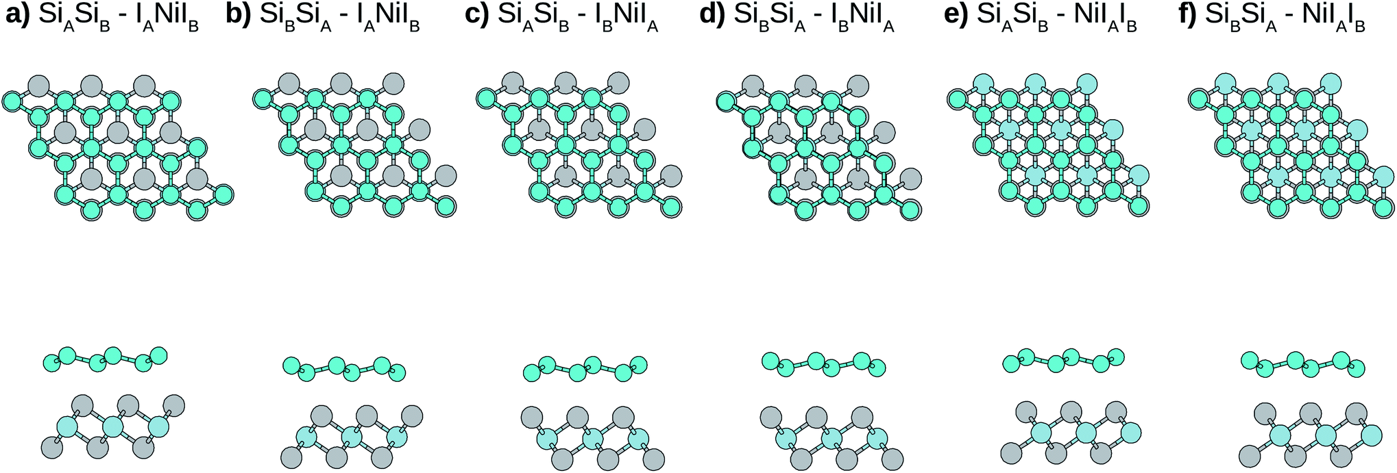 | ||
| Fig. 2 Top (top panel) and side (bottom panel) views of the six Si/NiI2 vdW heterostructure stacking configurations. In the stacks from (a) to (d), there is an I atom in the hollow site of the silicene hexagons, while in stacks (e) and (f), the Ni is in the hollow site of the silicene hexagon. Stacks (a) and (b) differ from (c) and (d) due to the fact that in stacks (a) and (b) the I atom in the silicene hexagon is the nearest atom to the silicene structure, while in stacks (c) and (d) it is the farthest atom. The (e) and (f) stacks differ from each other by the Si–I distance. Turquoise spheres represent Si atoms, while gray and light blue spheres represent I and Ni atoms, respectively. | ||
Initially we optimize the structures (including the lattice parameters), and the main parameters are shown in Table 1. It can be noted that, due to the interaction with the NiI2 monolayer, the silicene structure is slightly modified (mainly buckling) when compared with silicene in the free standing form.
| Configuration | dSi–Si (Å) | ΔSi–Si (Å) | h0 (Å) | Eb (eV) |
|---|---|---|---|---|
| SiASiB-IANiIB | 2.297 (2.294) | 0.540 (0.446) | 3.060 (3.712) | −0.281 (−0.024) |
| SiBSiA-IANiIB | 2.291 (2.295) | 0.524 (0.446) | 3.140 (3.729) | −0.266 (−0.018) |
| SiASiB-IBNiIA | 2.304 (2.299) | 0.577 (0.466) | 3.194 (3.867) | −0.237 (−0.016) |
| SiBSiA-IBNiIA | 2.287 (2.297) | 0.506 (0.404) | 4.068 (4.633) | −0.184 (−0.022) |
| SiASiB-NiIBIA | 2.285 (2.294) | 0.499 (0.438) | 3.519 (4.404) | −0.192 (−0.014) |
| SiBSiA-NiIBIA | 2.292 (2.297) | 0.587 (0.456) | 3.809 (3.960) | −0.231 (−0.019) |
To better understand the stacking stability of the vdW heterostructure, we calculated the binding energies (Eb), which describe the interaction strength between silicene and the substrate (NiI2 monolayer). The binding energy is estimated using the following equation:
| Eb = ESi2/NiI2 − (ESi2 + ENiI2), | (3) |
To analyze the effects of the cohesive forces, we also show the results without vdW interaction in parentheses in Table 1. As can be seen, the cohesive forces do not change the main qualitative results (the order of the stability of different stacking configurations), however the binding energies are mainly determined by cohesive forces. From Table 1 we can observe that circa 80% of the binding energies come from the cohesive forces, so a functional that encompasses the vdW interactions is essential to correctly describe the heterostructure system, as already observed for other bilayer systems.51
For the most stable stacking configuration, the band electronic structures obtained with different exchange–correlation functionals, PBE+DF2-c09, PBE+SOC+Grimme, and standard PBE, are shown in Fig. 3(a)–(c), respectively. The calculations with vdW interactions (Fig. 3(a) and (b)) show that the system is a semimetal for majority and minority spins. The Fermi energy (EF) touches states that form the top of the valence band (K and Γ points) for the majority spin and the bottom of the conduction band (along the K–M line) for the minority spin. We can also observe that when SOC (Fig. 3(b)) is added to the calculations, there is a splitting of states near the top of the valence band, mainly at the Γ-point. For the calculation without vdW corrections (Fig. 3(c)), semimetal behavior is obtained only for the minority spin. For the majority spin, we observe a small and direct band gap at the K-point.
 | ||
| Fig. 3 The calculated electronic band structures for the vdW structure in the most stable stacking configuration. The blue and red lines indicate majority and minority spin channels, respectively. For SOC calculations, the out-of-plane spin component Sz is indicated by colors of different intensity. | ||
When we compare the electronic band structures for the vdW heterostructure and the isolated systems, Fig. 3 and 1, we observe that near to the EF at the K-point of the BZ, there are four electronic states (two occupied and two empty) with dispersions that resemble the π and π* states in silicene. Inside these π-like states there are two electronic states (spin down) that resemble states in the NiI2 layer. The analysis of the p-DOS (see ESI Fig. 2†) confirms that these four states come from the silicene while the two inside states come from the NiI2 layer. In Fig. 3 we can also see that the energy gap between the π and π* states is different for the spin up and spin down channels. As shown before, the use of U and J parameters increases the energy separation between occupied and empty states of the NiI2 single layer. In the vdW heterostructure the empty states (spin down) from NiI2 are within the π and π* states of the silicene, so the use of U and J terms must change this scenario. In fact, when we use different values of U and J to correct the energetic positions of the d electrons from the Ni atom, we observe that these two states move to higher energies and can resonate with the π* states. However, the system continues to show a spin-polarized band gap between the π and π* states at the K point, as can be seen in ESI Fig. 3.†
From the calculations with different vdW functionals and SOC, we can infer that the interlayer interaction is the cause of an energy band gap between the π and π* states, as already observed for silicene integrated with other layered materials to form vdW heterostructures.24,25,28 The presence of a band gap between the π and π* states in a vdW heterostructure is associated with breaking the inversion symmetry of the two sublattices, and the greater the interaction, the greater the band gap. This effect is certainly the main one responsible for the band gap, but on its own, it does not explain why the two spin channels have different band gaps.
To analyze the causes of the spin-polarized band gap, initially we investigate how the interlayer interactions influence the band gap and can damage the linear dispersion of the π and π* states. These effects can be obtained by performing additional calculations with different values of the vertical distance (h) between layers. It is worth pointing out that control of the vertical distance between the layers in vdW heterostructures is experimentally possible.52–55
3.3 Vertical strain and charge transfer
The vertical strain effects on the electronic properties of the silicene/NiI2 heterostructure are investigated by increasing or decreasing the vertical distance between the two layers. We define the vertical strain as:
 | (4) |
Fig. 4 shows the effects on the electronic band structure near to the K-point of the vdW heterostructure when vertical strain is applied. As can be observed for positive vertical strain (Fig. 4(d)–(f)), the interlayer interaction becomes weak and the band gap decreases slowly. Actually, for large vertical strain (ε > 0.15), the VBM and the CBM near to the K-point recover their features for the silicene structure (an almost linear dispersion). However, for negative vertical strain (Fig. 4(a)–(c)), the band gap between the π states increases due to a major interaction between the layers. For εh > 0.10 (Fig. 4(e) and (f)), the linear dispersion of the π states near to the K-point is damaged due to the strong interlayer interaction. From Fig. 4 we can infer that the interlayer interaction is responsible for the band gap between the π and π* states. However, a more detailed investigation is necessary to understand the different gaps for the two spin channels. These properties also indicate that the charge densities for spin up and spin down must be different and depend on εh.
 | ||
| Fig. 4 Calculated electronic band structures near to the K-point for the vdW heterojunction with vertical strain (εh). Positive values of εh correspond to tensile strain, while negative values of εh correspond to compressive strain. The blue and red lines represent majority and minority π-like spin channels, respectively. The grey lines indicate states from the NiI2 layer. | ||
To understand the atypical electronic properties of the silicene/NiI2 vdW heterostructure we use the Löwdin population charge to analyze the charge transfer between layers. We observe that there is a net flow of charge from the NiI2 layer to silicene, as shown in Fig. 5(a). The charge transfer increases (decreases) for positive (negative) values of εh. However, when we separately analyze the charge transfer for the two spin channels, we observe that the charge for spin up flows from NiI2 to silicene, while the charge for spin down flows in the opposite direction. The different directions of the spin-polarized charge density cause the silicene to be spin-polarized, as can be observed in Fig. 5(b). The calculation of charge transfer shows that the SiA atom (below a Ni atom) has ρup > ρdown, while SiB (below an IB atom) has ρup < ρdown. In the equilibrium geometry, the calculated magnetic moment for the vdW heterostructure is 2 μB (the same as for the isolated NiI2 layer), and the two Si atoms contribute 0.01 μB. When εh reaches 0.15 the two Si atoms contribute 0.02 μB to the magnetic moment. The different directions of charge flow for spin up and spin down break the inversion symmetry of the two Si atoms and cause the π and π* states to exhibit a spin-dependent band gap.
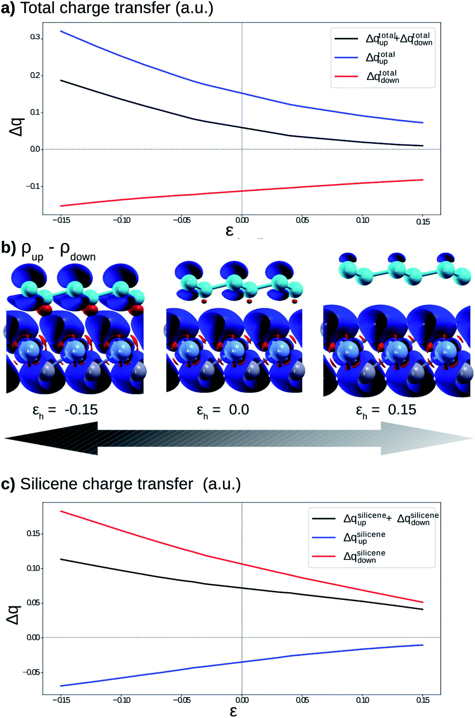 | ||
| Fig. 5 (a) Calculated charge transfer from NiI2 to silicene as a function of εh; (b) difference in the electronic charge densities with isovalue of 0.007 between spin up and spin down (Δρ = ρup − ρdown) when εh = −0.15, 0.0 and 0.15, the blue and red surfaces indicate positive and negative values, respectively; and (c) the charge difference ΔqSi in the two Si atoms. In parts (a) and (c), the black, blue and red lines refer to total, up and down charge, respectively. | ||
To confirm that the different spin-polarized charge densities on the Si atom are responsible for the atypical band gap between the π and π* states, again using the Löwdin population charge, we analyze the difference in the spin charge densities between the two Si atoms as a function of εh, and the results are shown in Fig. 5(c). From this figure we can observe that in absolute values the difference for charge down  is greater than the difference for charge up
 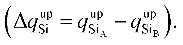 Again, this difference increases (decreases) for positive (negative) values of εh. The greater values of Δqdown compared to Δqup enable us to explain why the band gap between the π and π* states is different for the two spin channels (Edowng > Eupg).
From these results we can infer that the substrate (NiI2 layer) not only breaks the geometric inversion symmetry of the two Si atoms in the silicene structure but also breaks the spin inversion symmetry of the two Si atoms. Such effects show the possibility of using this vdW heterostructure in spin electronic devices (spintronics) by controlling the spin effects on the π and π* states. As already shown in previous studies on vdW heterostructures,28 the vertical strain (εh) is a feasible and powerful tool to adjust the interlayer interaction, and in this work we show that for silicene integrated with a FM layer (NiI2) to form a vdW heterostructure, εh also controls the band gap between the π and π* states for different spin channels.
4 Conclusion
First principles calculations based on DFT are used to perform a comprehensive investigation on the structural and electronic properties of a vdW heterostructure formed when a 2D FM semiconductor (NiI2) is integrated with silicene. The binding energy calculations show that the most stable configuration occurs in the SiASiB-IANiIB stacked bilayer. In this stacking configuration, one I atom is in the hollow site of the silicene (center of a hexagon) while the other two atoms (I and Ni) are on top of Si atoms.The total energy calculations show that the cohesive forces (vdW interactions) determine the interlayer interaction as well as the binding energies. The NiI2 single layer generates an inhomogenous potential acting on silicene and creates a small band gap between the π and π* states, which is different for the majority and minority spin channels. The fact that the two spin channels present different electronic band gaps is very important for the use of this vdW heterostructure in spintronics devices.
In this vdW heterostructure, two flat states (spin down) from the NiI2 single layer are inside the linear band gap when PBE and PBE+vdW are used to modulate the εxc functional. When DFT+U is used, the flat states move to higher energies and can resonate with the π* states. For spintronics devices, states inside the band gap should be avoided, however in the silicene/NiI2 vdW heterostructure the electrons localized in the flat states should have a larger effective mass (small mobility) then electrons localized in the states with linear dispersion from the silicene. So the conductance must occur primarily between the silicene states, and only a residual current must be observed in the NiI2 single layer.
The analysis of the charge density reveals that there is a net charge transfer from NiI2 to silicene. The direction of the charge transfer flow is different for spin up and spin down, which leads to the two Si atoms being spin-polarized. Furthermore, using vertical strain, the interlayer distance can be adjusted, and the charge transfer as well as the band gap can be controlled.
In summary, due to the fact that there is an adjustable spin charge flow between the layers, we show that a single layer of NiI2 integrated with silicene to form a vdW heterostructure is a potential material to be used in spintronics, once a spin-dependent current mobility is obtained.
Conflicts of interest
There are no conflicts to declare.Acknowledgements
This study was financed in part by the Coordenação de Aperfeiçoamento de Pessoal de Nível Superior – Brasil (CAPES) – Finance Code 001 – and in part by CNPq. The authors also acknowledge CENAPAD/SP and CEPAD/UFSM for the computational time. We also thank Professor R. Ahuja from Uppsala University for the discussions during his visit to the Federal University of Santa Maria.Notes and references
- K. S. Novoselov, A. K. Geim, S. V. Morozov, D. Jiang, Y. Zhang, S. V. Dubonos, I. V. Grigorieva and A. A. Firsov, Science, 2004, 306, 666–669 CrossRef PubMed.
- A. C. Neto, F. Guinea, N. M. Peres, K. S. Novoselov and A. K. Geim, Rev. Mod. Phys., 2009, 81, 109 CrossRef.
- P. Vogt, P. De Padova, C. Quaresima, J. Avila, E. Frantzeskakis, M. C. Asensio, A. Resta, B. Ealet and G. Le Lay, Phys. Rev. Lett., 2012, 108, 155501 CrossRef PubMed.
- Z.-X. Guo, S. Furuya, J.-i. Iwata and A. Oshiyama, Phys. Rev. B: Condens. Matter Mater. Phys., 2013, 87, 235435 CrossRef.
- H. Jamgotchian, Y. Colignon, N. Hamzaoui, B. Ealet, J. Hoarau, B. Aufray and J. Bibérian, J. Phys.: Condens. Matter, 2012, 24, 172001 CrossRef CAS.
- M. J. Cherukara, B. Narayanan, H. Chan and S. K. Sankaranarayanan, Nanoscale, 2017, 9, 10186–10192 RSC.
- S. Cahangirov, M. Topsakal, E. Aktürk, H. Şahin and S. Ciraci, Phys. Rev. Lett., 2009, 102, 236804 CrossRef.
- C.-C. Liu, W. Feng and Y. Yao, Phys. Rev. Lett., 2011, 107, 076802 CrossRef.
- J. Zhao, H. Liu, Z. Yu, R. Quhe, S. Zhou, Y. Wang, C. C. Liu, H. Zhong, N. Han and J. Lu, et al., Prog. Mater. Sci., 2016, 83, 24–151 CrossRef.
- C. Xu, G. Luo, Q. Liu, J. Zheng, Z. Zhang, S. Nagase, Z. Gao and J. Lu, Nanoscale, 2012, 4, 3111–3117 RSC.
- J. Zhu, A. Chroneos and U. Schwingenschlögl, Nanoscale, 2016, 8, 7272–7277 RSC.
- Z. Ni, Q. Liu, K. Tang, J. Zheng, J. Zhou, R. Qin, Z. Gao, D. Yu and J. Lu, Nano Lett., 2012, 12, 113–118 CrossRef.
- N. Drummond, V. Zolyomi and V. Fal’Ko, Phys. Rev. B: Condens. Matter Mater. Phys., 2012, 85, 075423 CrossRef.
- R. Quhe, R. Fei, Q. Liu, J. Zheng, H. Li, C. Xu, Z. Ni, Y. Wang, D. Yu and Z. Gao, et al., Sci. Rep., 2012, 2, 853 CrossRef PubMed.
- Z. Ni, H. Zhong, X. Jiang, R. Quhe, G. Luo, Y. Wang, M. Ye, J. Yang, J. Shi and J. Lu, Nanoscale, 2014, 6, 7609–7618 RSC.
- B. Mohan, A. Kumar and P. Ahluwalia, Phys. E., 2014, 61, 40–47 CrossRef.
- J.-A. Yan, S.-P. Gao, R. Stein and G. Coard, Phys. Rev. B: Condens. Matter Mater. Phys., 2015, 91, 245403 CrossRef.
- D. Tsoutsou, E. Xenogiannopoulou, E. Golias, P. Tsipas and A. Dimoulas, Appl. Phys. Lett., 2013, 103, 231604 CrossRef.
- C.-L. Lin, R. Arafune, K. Kawahara, M. Kanno, N. Tsukahara, E. Minamitani, Y. Kim, M. Kawai and N. Takagi, Phys. Rev. Lett., 2013, 110, 076801 CrossRef.
- N. Gao, J. Li and Q. Jiang, Chem. Phys. Lett., 2014, 592, 222–226 CrossRef CAS.
- S.-s. Li, C.-w. Zhang, S.-s. Yan, S.-j. Hu, W.-x. Ji, P.-j. Wang and P. Li, J. Phys.: Condens. Matter, 2014, 26, 395003 CrossRef.
- R. Quhe, Y. Yuan, J. Zheng, Y. Wang, Z. Ni, J. Shi, D. Yu, J. Yang and J. Lu, Sci. Rep., 2015, 4, 5476 CrossRef.
- H. Liu, J. Gao and J. Zhao, J. Phys. Chem. C, 2013, 117, 10353–10359 CrossRef CAS.
- H. Zhao, C. Zhang, S. Li, W. Ji and P. Wang, J. Appl. Phys., 2015, 117, 085306 CrossRef.
- C. Jin, Y. Dai, W. Wei, Q. Sun, X. Li and B. Huang, RSC Adv., 2017, 7, 5827–5835 RSC.
- Y. Fan, X. Liu, J. Wang, H. Ai and M. Zhao, Phys. Chem. Chem. Phys., 2018, 20, 11369–11377 RSC.
- H. Xue, Y. Dai, W. Kim, Y. Wang, X. Bai, M. Qi, K. Halonen, H. Lipsanen and Z. Sun, Nanoscale, 2019, 11, 3240–3247 RSC.
- W. Xia, L. Dai, P. Yu, X. Tong, W. Song, G. Zhang and Z. Wang, Nanoscale, 2017, 9, 4324–4365 RSC.
- M. McGuire, Crystals, 2017, 7, 121 CrossRef.
- V. V. Kulish and W. Huang, J. Mater. Chem. C, 2017, 5, 8734–8741 RSC.
- N. Mounet, M. Gibertini, P. Schwaller, D. Campi, A. Merkys, A. Marrazzo, T. Sohier, I. E. Castelli, A. Cepellotti and G. Pizzi, et al., Nat. Nanotechnol., 2018, 13, 246 CrossRef CAS.
- M. Lu, Q. Yao, C. Xiao, C. Huang and E. Kan, ACS Omega, 2019, 4, 5714–5721 CrossRef CAS.
- P. Hohenberg and W. Kohn, Phys. Rev., 1964, 136, B864 CrossRef.
- W. Kohn and L. J. Sham, Phys. Rev., 1965, 140, A1133 CrossRef.
- P. Giannozzi, S. Baroni, N. Bonini, M. Calandra, R. Car, C. Cavazzoni, D. Ceresoli, G. L. Chiarotti, M. Cococcioni and I. Dabo, et al., J. Phys.: Condens. Matter, 2009, 21, 395502 CrossRef.
- P. Giannozzi, O. Andreussi, T. Brumme, O. Bunau, M. B. Nardelli, M. Calandra, R. Car, C. Cavazzoni, D. Ceresoli and M. Cococcioni, et al., J. Phys.: Condens. Matter, 2017, 29, 465901 CrossRef CAS.
- J. P. Perdew, K. Burke and M. Ernzerhof, Phys. Rev. Lett., 1996, 77, 3865 CrossRef CAS.
- K. Lee, É. D. Murray, L. Kong, B. I. Lundqvist and D. C. Langreth, Phys. Rev. B: Condens. Matter Mater. Phys., 2010, 82, 081101 CrossRef.
- V. R. Cooper, Phys. Rev. B: Condens. Matter Mater. Phys., 2010, 81, 161104 CrossRef.
- A. M. Rappe, K. M. Rabe, E. Kaxiras and J. Joannopoulos, Phys. Rev. B: Condens. Matter Mater. Phys., 1990, 41, 1227 CrossRef.
- H. J. Monkhorst and J. D. Pack, Phys. Rev. B: Condens. Matter Mater. Phys., 1976, 13, 5188 CrossRef.
- S. Kuindersma, P. Boudewijn and C. Haas, Phys. Status Solidi B, 1981, 108, 187–194 CrossRef CAS.
- A. S. Botana and M. R. Norman, Phys. Rev. Mater., 2019, 3, 044001 CrossRef CAS.
- R. Skomski, D. Sander, J. Shen and J. Kirschner, J. Appl. Phys., 1997, 81, 4710–4712 CrossRef CAS.
- M. P. Pasternak, R. D. Taylor, A. Chen, C. Meade, L. Falicov, A. Giesekus, R. Jeanloz and Y. Y. Peter, Phys. Rev. Lett., 1990, 65, 790 CrossRef CAS.
- H. Starnberg, M. Johnson and H. Hughes, J. Phys. C: Solid State Phys., 1986, 19, 2689 CrossRef CAS.
- C. Ronda, G. Arends and C. Haas, Phys. Rev. B: Condens. Matter Mater. Phys., 1987, 35, 4038 CrossRef CAS.
- S.-H. Lin and J.-L. Kuo, Phys. Chem. Chem. Phys., 2014, 16, 20763–20771 RSC.
- H. Sahin and F. M. Peeters, Phys. Rev. B: Condens. Matter Mater. Phys., 2013, 87, 085423 CrossRef.
- Q. Xu, G. Yang, X. Fan and W. Zheng, Phys. Chem. Chem. Phys., 2019, 21, 4276–4285 RSC.
- F. Schulz, P. Liljeroth and A. P. Seitsonen, Phys. Rev. Mater., 2019, 3, 084001 CrossRef CAS.
- A. K. Kleppe, M. Amboage and A. P. Jephcoat, Sci. Rep., 2015, 4, 4989 CrossRef.
- W. Fan, X. Zhu, F. Ke, Y. Chen, K. Dong, J. Ji, B. Chen, S. Tongay, J. W. Ager and K. Liu, et al., Phys. Rev. B: Condens. Matter Mater. Phys., 2015, 92, 241408 CrossRef.
- P. Ci, Y. Chen, J. Kang, R. Suzuki, H. S. Choe, J. Suh, C. Ko, T. Park, K. Shen and Y. Iwasa, et al., Nano Lett., 2017, 17, 4982–4988 CrossRef CAS.
- X. Fu, F. Li, J.-F. Lin, Y. Gong, X. Huang, Y. Huang, H. Gao, Q. Zhou and T. Cui, J. Phys. Chem. C, 2018, 122, 5820–5828 CrossRef CAS.
Footnote |
| † Electronic supplementary information (ESI) available. See DOI: 10.1039/c9ra10199c |
| This journal is © The Royal Society of Chemistry 2020 |