
 Open Access Article
 This Open Access Article is licensed under a Creative Commons Attribution-Non Commercial 3.0 Unported Licence
A high performance surface acoustic wave visible light sensor using novel materials: Bi2S3 nanobelts
Chong Li†
a,
Hao Kan†ab,
Jingting Luo *a,
Chen Fu*a,
Jian Zhouc,
Xueli Liud,
Wen Wangd,
Qiuping Weie and
Yongqing Fuf
*a,
Chen Fu*a,
Jian Zhouc,
Xueli Liud,
Wen Wangd,
Qiuping Weie and
Yongqing Fuf
aShenzhen Key Laboratory of Advanced Thin Films and Applications, College of Physics and Optoelectronic Engineering, Shenzhen University, 518060, Shenzhen, China. E-mail: luojt@szu.edu.cn; chenfu@szu.edu.cn
bKey Laboratory of Optoelectronic Devices and Systems of Ministry of Education and Guangdong Province, College of Optoelectronic Engineering, Shenzhen University, 518060, Shenzhen, China
cState Key Laboratory of Advanced Design and Manufacturing for Vehicle Body, College of Mechanical and Vehicle Engineering, Hunan University, Changsha 410082, China
dInstitute of Acoustics, Chinese Academy of Sciences, 100190, Beijing, China
eSchool of Materials Science and Engineering, State Key Laboratory of Powder Metallurgy, Central South University, Changsha 410083, China
fFaculty of Engineering and Environment, Northumbria University, Newcastle upon Tyne, NE1 8ST, UK
First published on 2nd March 2020
Abstract
Low dimensional Bi2S3 materials are excellent for use in photodetectors with excellent stability and fast response time. In this work, we developed a visible light sensor with good performance based on surface acoustic wave (SAW) devices using Bi2S3 nanobelts as the sensing materials. The SAW delay-line sensor was fabricated on ST-cut quartz with a designed wavelength of 15.8 microns using conventional photolithography techniques. The measured center frequency was 200.02 MHz. The Bi2S3 nanobelts prepared by a facile hydrothermal process were deposited onto SAW sensors by spin-coating. Under irradiation of 625 nm visible light with a power intensity of 170 μW cm−2, the sensor showed a fast and large response with a frequency upshift of 7 kHz within 1 s. The upshift of the frequency of the SAW device is mainly attributed to the mass loading effect caused by the desorption of oxygen from the Bi2S3 nanobelts under visible light radiation.
Introduction
Over the past few decades, Surface Acoustic Wave (SAW) devices have been widely used in industrial fields for components such as radio frequency filters and oscillators.1 They can be effectively produced by fabricating interdigital transducers (IDTs) on the surface of piezoelectric substrates.2 SAW devices have the advantages of good stability, low power consumption and wireless transmission, etc, and they are also very sensitive to any external stimulation or changes on the surface. Therefore, SAW devices have great potential to be used as biosensors, gas sensors, pressure sensors, photodetectors and so on.3–8In recent years, photodetectors based on SAW devices have received extensive attention.9–11 For example, Pang et al. fabricated a LiTaO3-based Love mode SAW ultraviolet (UV) sensor with ZnO top layer,12 which was operated at a resonant frequency of 41.5 MHz, with a frequency shift of 150 kHz under 254 nm UV radiation at 350 μW cm−2 Zhou et al. used MoS2 nanosheets as the UV-sensitive layer for SAW photodetectors,8 which showed a maximum frequency shift of 3.5 MHz under a 365 nm UV illumination at a power density of 1.466 mW cm−2. However, there are few reports about visible-light sensors or infrared sensors based on the SAW devices. These photodetectors can be extensively used in electronic eyes,13 tumor detection,14 and imaging.15
Bismuth sulfide (Bi2S3) is one of the important group V and VI binary chalcogenide semiconductors with a narrow band-gap of 1.3 eV, good environmental stability and large absorption coefficient. It has been widely used in solar cells, photocatalytic and so on.16–18 Furthermore, it has an orthorhombic structure which has an inherent anisotropic crystal structure along the [001] direction, thus making it possible for the preferential growth into 1D nanostructure.19 For example, Yu et al. synthesized uniform Bi2S3 nanorods with tuneable lengths, which exhibited excellent responses to visible light.20 Li et al. prepared Bi2S3 hollow sphere nanostructures using a hydrothermal method.21 The photoconductivity of the photodetector made using these hollow spheres demonstrated excellent stability and fast response time towards visible light. Konstantatos prepared solution-processed photoconductive detector based on Bi2S3 nanocrystals, which showed good responsivity (40 A W−1) under visible light radiation.22 However, there are no reports about SAW photodetectors based on Bi2S3 nanomaterials. It is critical to develop such a high performance photodetector based on SAW resonator using Bi2S3 nanomaterials, which will have advantages of wireless control, battery-less operation and high sensitivity because of the merits from SAW devices.
In this work, we demonstrated, for the first time, a high performance surface acoustic wave visible light photodetector using novel materials: Bi2S3 nanobelts. In our strategy, Bi2S3 nanobelts were synthesized using a hydrothermal method and then spin-coated onto a ST-cut quartz SAW device. The SAW device had very good response to the visible light and the sensing mechanisms were discussed.
Experimental section
Material synthesis
Bi2S3 nanobelts were prepared using a hydrothermal method reported in the literature.23 Briefly, triphenyl bismuth (C18H15Bi, 98%, Aladdin, 0.6 mM) and dibenzyl disulfide (C6H5CH2SSCH2C6H5, 98%, Aladdin, 0.6 mM) were dissolved in 4 ml oleylamine (OLA), and then 0.4 g polyvinyl pyrrolidone (PVP, Aladdin, MW ≈ 24![[thin space (1/6-em)]](https://www.rsc.org/images/entities/char_2009.gif) 000–28000) were dissolved into 26 ml absolute ethanol. After that, these solutions were thoroughly mixed together and transferred into a 50 ml autoclave to react at 180 °C for 8 hours. Finally, the product was washed with hexane and dissolved in ethanol at a concentration of 30 mg ml−1 for use.
000–28000) were dissolved into 26 ml absolute ethanol. After that, these solutions were thoroughly mixed together and transferred into a 50 ml autoclave to react at 180 °C for 8 hours. Finally, the product was washed with hexane and dissolved in ethanol at a concentration of 30 mg ml−1 for use.
Sensor fabrication and measurements
Quartz is a widely used piezoelectric material, which has a low temperature coefficient, low sound velocity and very good stability. In this study, a ST-cut quartz is chosen as the piezoelectric substrate for making the SAW delay-line device. A schematic diagram is shown in Fig. 1a. The input IDTs consist of 220 finger pairs and the output IDTs have 95 finger pairs. The sensitive area of the SAW device is 3.6 mm2. All the aluminium based IDTs were fabricated through a conventional photolithography technique. The measured center frequency was 200.02 MHz. The obtained optical microscope image of the device is shown in Fig. 1b.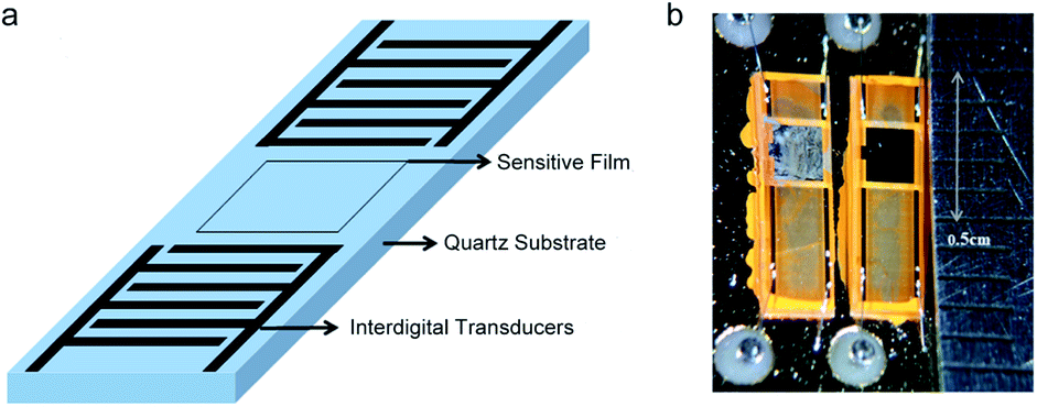 | ||
| Fig. 1 (a) A schematic illustration, and (b) an optical microscope image of the ST-cut quartz SAW device. | ||
For the sensitive layer deposition, 50 μL of Bi2S3 nanobelts solution was spin-coated (at a speed of 1500 rpm) onto the sensitive area of the SAW resonator as a photosensitive material. The central frequency of SAW delay-line device was measured using a network analyzer (Keysight, E5071C). A 625 nm light-emitting diode was precisely controlled through a functional generator (JDS6600) for acting as a light source. The intensity of the incident light was measured using a power meter (Thermo Fisher Scientific). A schematic illustration of the testing system was shown in Fig. 2.
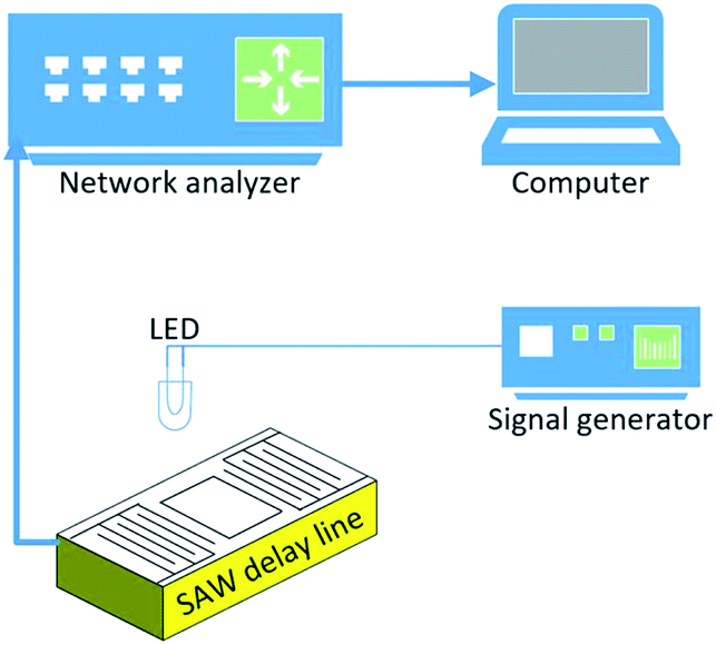 | ||
| Fig. 2 Schematic illustration of the experimental setup. | ||
Microstructures of the sensing material were studied using a field emission scanning electron microscopy (FE-SEM, Supra 55 Sapphire) and a high-resolution transmission electron microscopy (HR-TEM, JEOL-2100). Crystallization of the Bi2S3 nanobelts were characterized using the X-ray diffraction (XRD, Ultima IV) with CuKα radiation that was operated at 30 kV and 30 mA. The UV-Vis absorption spectrum was measured using a UV/Vis/NIR spectrometer (PerkinElmer Lambda 950).
Results and discussion
Microstructure and morphology of the samples
A low-magnification and a high-magnification SEM image are shown in Fig. 3a and b, respectively, which revealed 1-D belt-shaped structure of as-synthesized Bi2S3. The average length of the synthesized nanobelts is about five to twenty micrometres and the width is about fifty to three hundred nanometres. A uniform and porous layer formed on the sensitive area of the quartz substrate. TEM image provides detailed information about the morphology and the structural features of the as-synthesized Bi2S3 nanobelts, e.g., a 1-D strip-like nanostructure shown in Fig. 3c. The HR-TEM image in Fig. 3d clearly shows the lattice spacing of 0.353 nm, which corresponds to the (310) planes of orthorhombic Bi2S3 phase.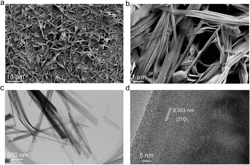 | ||
| Fig. 3 SEM image of the Bi2S3 nanobelts film (a) at low magnification (b) at high magnification. (c) TEM image and (d) HR-TEM image of the Bi2S3 nanobelts. | ||
Fig. 4a shows a typical XRD pattern of the Bi2S3 nanobelts. Clearly, all the diffraction peaks are consistent with the orthorhombic structure of bulk Bi2S3 (JCPDS card no. 17-0320). These is no extra diffraction peaks from other materials, which indicates that high-purity Bi2S3 nanomaterials were synthesized. Fig. 4b demonstrates the UV-Vis absorption spectrum of the Bi2S3 nanobelts, which have an obvious and broad optical absorption peak from 300–700 nm, implying their potentials for applications in UV-Vis photodetectors.
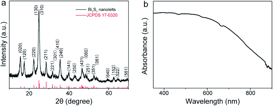 | ||
| Fig. 4 (a) XRD pattern of the prepared Bi2S3 nanobelts. (b) UV-visible absorption spectrum of Bi2S3 nanobelts. | ||
Visible light sensing performance
Fig. 5 shows the transmission signals (S12) of resonant frequencies of SAW delay-line device with and without Bi2S3 nanobelts sensing layer. The central frequency of the SAW device as fabricated is 200.02 MHz and the insertion loss is −12.82 dB. After coating Bi2S3 nanobelts film, the central frequency decreased and the insertion loss increased as the result of the mass loading effect and the wave diffraction due to the addition of Bi2S3 nanobelts film.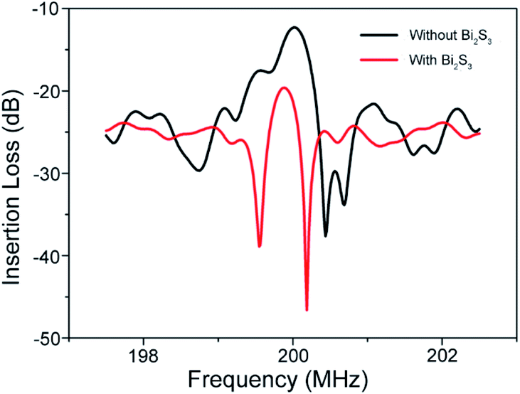 | ||
| Fig. 5 Measured transmission signals (S12) of resonant frequencies for the SAW device with and without Bi2S3 nanobelts. | ||
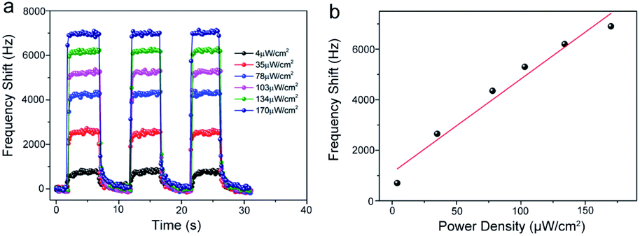
Fig. 6a shows frequency evolution curves of the SAW visible light sensor under different light intensities with a wavelength of 625 nm. Clearly, the sensor exhibits a positive frequency shift when the light switch on and the working frequency of the SAW device recover to its initial value when the light switch off. Upon three repeated on/off cycles using the LED, the dynamic response curves for three cycles are almost identical with each other under the same light intensity. This result indicates that the SAW visible light sensor using Bi2S3 nanobelts has good repeatability and reproducibility. In addition, the frequency shifts of the sensor are increased with the increase of visible light power density. The frequency-shifts as large as 7 kHz when the light intensity increased to 170 μW cm−2. The curve of the frequency-shifts dependence on light intensity was plotted in Fig. 6b. The frequency-shifts are enhanced with increasing light intensity and will not show any saturation due to the low density of the incident light. The frequency-shift of the device is 300 Hz, even under the illumination with an optical power as low as 4 μW cm−2.
 | ||
| Fig. 6 (a) Photo responses of the SAW photodetector based on Bi2S3 nanobelts under 625 nm visible light with different power densities. (b) The dependence of frequency shift on power intensities under 625 nm visible light. | ||
The sensitivities (S) is the most important parameter for SAW photodetector, it can be calculated from the following equation.
 | (1) |
| Materials | Piezoelectric substrate | Central frequency | Wavelength | Sensitivity (ppm (μW cm−2)−1) | Ref. |
|---|---|---|---|---|---|
| ZnO film | LiNbO3 | 36.3 MHz | 365 nm | 0.12 | 28 |
| ZnO nanoparticles | YZ LiNbO3 | 64 MHz | 345 nm | 2.8 | 29 |
| ZnO nanowire | 128° YX LiNbO3 | 50.9 MHz | 365 nm | 8.765 | 30 |
| ZnO nanoparticles | 128° YX LiNbO3 | 235 MHz | 365 nm | 3.34 | 31 |
| MoS2 nanosheets | ZnO | 1.02 GHz | 365 nm | 2.05 | 8 |
| Bi2S3 nanobelts | ST-cut quartz | 200.02 MHz | 625 nm | 0.2 | This work |
The central frequency shift of the SAW light sensor can be ascribe to the acousto-electric interaction effect, mass-loading effect and the elastic effect.24 Generally, under visible light radiation, the photo-generated carries will decrease the SAW velocity due to acoustoelectric effect,25 and hence the SAW central frequency will downshift. However, the central frequency is upshift under visible light radiation in our experiment. Therefore, the acoustoelectric effect can't be the dominated reason for this work. It should be noted in our work that the ST-cut quartz substrate have a low electro-mechanical coupling coefficient, e.g., k2 = 0.11%.26 Therefore, the acoustoelectric effect may have a low effect on our SAW device.
On the other hand, the mass-loading effect result in a change in frequency shift (Δf) is given by:27
| Δf = −cmf02Δms | (2) |
In this work, we suggest the photo response of Bi2S3 nanobelts related to the oxygen adsorption and desorption on Bi2S3 nanomaterials. Fig. 7 shows a schematic illustration of adsorption and desorption of oxygen on Bi2S3 nanobelts coated on IDT/quartz structure under dark and visible light radiation. Under a dark condition, oxygen molecules could capture free electrons from the nanobelts through the following equation.
| O2 + e− → O2− | (3) |
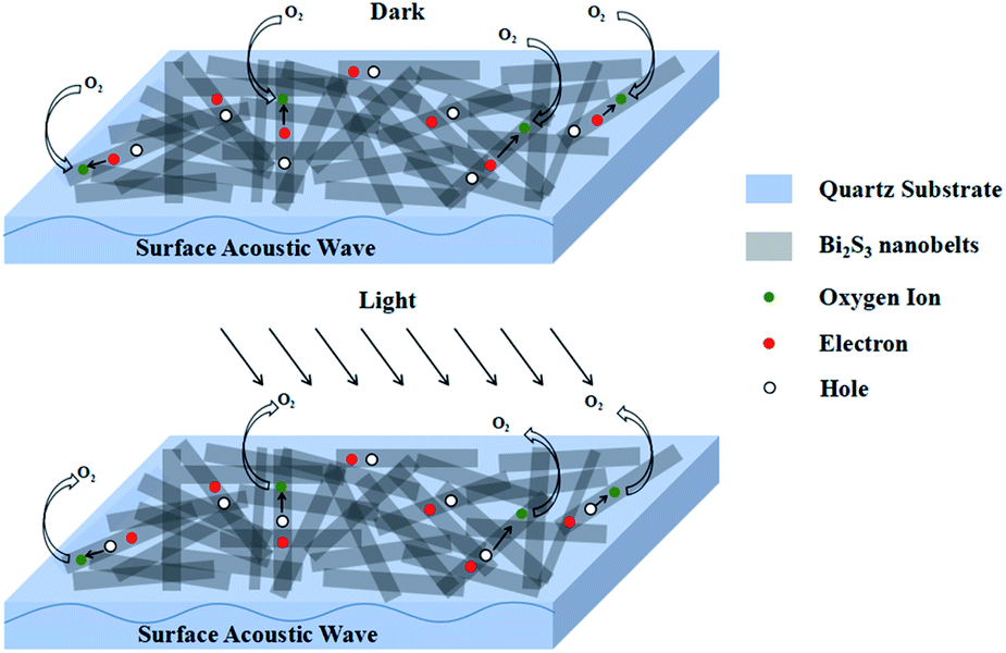 | ||
| Fig. 7 Schematic illustration of sensing mechanisms of adsorption and desorption of oxygen on Bi2S3 nanobelts. | ||
Upon illumination by visible light, there will be electron–hole pairs generated in the nanobelts. The adsorbed oxygen molecules on Bi2S3 nanobelts will capture the photo-generated holes, which discharged via a reaction as below.
| O2− + h+ → O2 | (4) |
Thereby the mass loading of the film reduced under light irradiation due to the oxygen discharge, which promotes the acoustic wave propagation and thus increase the central frequency. In this work, the Bi2S3 nanobelts films with lots of porous have contributed to the adsorption and desorption of oxygen molecules (Fig. 3a and b). Therefore, with increasing incident light intensity from 4 to 170 μW cm−2, more excited photo-carriers are produced by higher light intensity, thus more oxygen ions will be released. Therefore, the frequency shift will be larger. After the light switched off, oxygen ions will be re-absorbed again. Hence, the mass loading increased due to the oxygen re-absorption, which goes against the acoustic wave propagation and thus the centre frequency returns back.
Conclusions
In this work, we demonstrate a high performance SAW visible light sensor using novel materials, Bi2S3 nanobelts, for the first time. The frequency upshifts of the SAW photodetector reached as high as 7 kHz upon 625 nm with intensity of 170 μW cm−2. Further, the SAW visible light sensor exhibited a sensitivity of about 0.2 ppm (μW cm−2)−1 and a good linear characteristic within the range from 4 to 170 μW cm−2. Due to a low electro-mechanical coupling coefficient of ST-cut quartz SAW devices, the upshift of frequency of the SAW photodetector might not be ascribed to the acoustoelectric effect. On the other hand, the mass loading effect pay the main role in the upshift of frequency of the SAW photodetector caused by the desorption of oxygen from the Bi2S3 nanobelts under visible light radiation. This facile fabrication of a fast and large response SAW visible light sensor using Bi2S3 nanobelts offers a novel method for visible light photodetector devices in practical applications.Conflicts of interest
There are no conflicts to declare.Acknowledgements
The authors gratefully acknowledge the support of the National Key Research and Development Program of China (grant no. 2016YFB0402705), State Key Laboratory of Powder Metallurgy, Central South University, the China Postdoctoral Science Foundation (2019M653018). This work was also supported by National Natural Science Foundation of China (grant no. 11704261, 51605485, 11575118), Shenzhen Science & Technology Project (grant no. JCYJ20170817100658231, JCYJ20180507182439574, JCYJ20180305124317872). Funding supports from UK Engineering Physics and Science Research Council (EPSRC EP/P018998/1).References
- A. Pohl, IEEE Trans. Ultrason. Ferroelectrics Freq. Contr., 2000, 47, 317–331 Search PubMed.
- R. M. White and F. W. Voltmer, Appl. Phys. Lett., 1965, 7, 314–316 CrossRef.
- M. Goran, M. Tina, K. Wöllner and G. Gauglitz, Surf. Coat. Technol., 2006, 201, 1282–1288 CrossRef.
- Y. Q. Fu, J. K. Luo, N. T. Nguyen, A. J. Walton, A. J. Flewitt, X. T Zu, Y. Li, G. McHale, A. Matthews, E. Iborra, H. Du and W. I. Milne, Prog. Mater. Sci., 2017, 89, 31–91 CrossRef.
- Y. Liu, H. Huang, L. L. Wang, D. P. Cai, B. Liu, D. D. Wang, Q. H. Li and T. H. Wang, Electrospun CeO2 nanoparticles/PVP nanofibers based high-frequency surface acoustic wave humidity sensor, Sens. Actuators, B, 2016, 223, 730–737 CrossRef CAS.
- L. Rana, R. Gupta, R. Kshetrimayumb, M. Tomarc and V. Guptaa, Surf. Coat. Technol., 2018, 343, 89–92 CrossRef CAS.
- S. Liu, G. Xu, Z. Ni, X. Guo, L. Luo, J. Tu and D. Zhang, Appl. Phys. Lett., 2017, 111, 043508 CrossRef.
- P. Zhou, C. Chen, X. Wang, B. Hu and H. San, Sens. Actuators, A, 2018, 271, 389–397 CrossRef CAS.
- C. Fu, K. Lee, K. Lee and S. Yang, Smart Mater. Struct., 2015, 24, 01501 Search PubMed.
- M. Thepnurat, P. Ruankham, S. Phadunghitidhada, A. Gardchareon, D. Wongratanaphisan and S. Choopun, Surf. Coat. Technol., 2016, 306, 25–29 CrossRef CAS.
- W. Peng, Y. He, Y. Xu, S. Jin, K. Ma, X. Zhao, X. Kang and C. Wen, Sens. Actuators, A, 2013, 199, 149–155 CrossRef CAS.
- H. Pang, Y. Fu, Z. Li, Y. Li, J. Ma, F. Placido, A. J. Walton and X. Zu, Sens. Actuators, A, 2013, 193, 87–94 CrossRef CAS.
- H. Ko, M. P. Stoykovich, J. Song, V. Malyarchuk, W. M. Choi, C. Yu, J. B. Geddes, J. Xiao, S. Wang, Y. Huang and J. A. Rogers, Nature, 2008, 454, 748–753 CrossRef CAS.
- X. Gao, Y. Cui, R. M. Levenson, L. W. K. Chung and S. Nie, Nat. Biotechnol., 2004, 22, 969–976 CrossRef CAS PubMed.
- H. Kan, W. Zheng, R. Lin, M. Li, C. Fu, H. Sun, M. Dong, C. Xu, J. Luo, Y. Fu and F. Huang, ACS Appl. Mater. Interfaces, 2019, 11, 8412–8418 CrossRef.
- A. K. Rath, M. Bernechea, L. Martinez and G. Konstantatos, Adv. Mater., 2011, 23, 3712–3717 CrossRef PubMed.
- G. Li, X. Chen and G. Gao, Nanoscale, 2014, 6, 3283–3288 RSC.
- S. Vadivel, A. N. Naveen, V. P. Kamalakannan, P. Cao and N. Balasubramanian, Appl. Surf. Sci., 2015, 351, 635–645 CrossRef.
- M. B. Sigman and B. A. Korgel, Chem. Mater., 2005, 17, 1655–1660 CrossRef.
- H. Yu, J. Wang, T. Wang, H. Yu, J. Yang, G. Liu, G. Qiao, Q. Yang and X. Cheng, CrystEngComm, 2017, 19, 727–733 RSC.
- H. Li, J. Yang, J. Zhang and M. Zhou, RSC Adv., 2012, 2, 6258–6261 RSC.
- G. Konstantatos, L. Levina, J. Tang and E. H. Sargent, Nano Lett., 2008, 8, 4002–4006 CrossRef CAS.
- H. Kan, M. Li, Z. Song, S. Liu, B. Zhang, J. Liu, M. Li, G. Zhang, S. Jiang and H. Liu, J. Colloid Interface Sci., 2017, 506, 102–110 CrossRef CAS.
- J. D. Gailpeau, R. S. Falconer, J. F. Vetelino, J. J. Caron, E. L. Wittman, M. G. Schweyer and J. C. Andle, Sens. Actuators, B, 1995, 24, 49–53 CrossRef.
- A. J. Ricco, S. J. Martin and T. E. Zipperian, Sens. Actuators, B, 1985, 8, 319–333 CrossRef.
- L. Rana, R. Gupta, M. Tomar and V. Gupta, Sens. Actuators, B, 2017, 252, 840–845 CrossRef.
- J. D. N. Cheeke and Z. Wang, Sens. Actuators, B, 1999, 59, 146–153 CrossRef.
- P. Sharma and K. Sreenivas, Appl. Phys. Lett., 2003, 83, 3617 CrossRef.
- V. Chivukula, D. Ciplys, M. Shur and P. Dutta, Appl. Phys. Lett., 2010, 96, 233512 CrossRef.
- W. Peng, Y. He, C. Wen and K. Ma, Sens. Actuators, A, 2012, 184, 34–40 CrossRef CAS.
- K. J. Lee, H. Oh, M. Jo, K. Lee and S. Yang, Microelectron. Eng., 2013, 111, 105–109 CrossRef CAS.
Footnote |
| † These authors have equal contribution. |
| This journal is © The Royal Society of Chemistry 2020 |