DOI:
10.1039/C9RA09773B
(Paper)
RSC Adv., 2020,
10, 3105-3114
Modified top-down approach for synthesis of molybdenum oxide quantum dots: sonication induced chemical etching of thin films
Received
22nd November 2019
, Accepted 10th January 2020
First published on 17th January 2020
Abstract
A simple and modified top-down approach to synthesize molybdenum oxide (MoOx: x = 2, 3) quantum dots (QDs) is proposed in this study. This modified approach involves the conversion of a bulk powder material into thin films followed by a sonication induced chemical etching process for synthesising QDs. X-Ray Diffraction (XRD) is used for crystal structural characterization of MoOx thin films. The crystal structure properties of the MoOx QDs are analysed by High Resolution Transmission Electron Microscopy (HRTEM) images and corresponding Selected Area Electron Diffraction (SAED) patterns. The optical band gap is estimated by Tauc's plot from UV-Vis-NIR absorption spectra. The excitation dependent photoluminescence (PL) emission of MoOx QDs as a function of acid concentration is investigated. The growth mechanism of QDs in different crystalline phases as a function of acid concentration is also exemplified in this work. The micro-Raman and Fourier Transform of Infrared (FTIR) spectra are recorded to analyse the vibrational spectrum of the molybdenum–oxygen (Mo–O) bonds in the MoOx QDs.
Introduction
Transition Metal Oxide (TMO) nanostructures have shown great promise and are being investigated with great attention for basic scientific and industrial research owing to their unique physical and chemical properties.1–3 Among TMOs, molybdenum oxide (MoOx) based nano-materials with different morphologies have attracted great attention in recent years due to their optical, electronic, and structural features.4–13 One dimensional (1D) and two dimensional (2D) nano-belts,4,5 nano-rods,3,6 nano-wires,7,8 nano-flowers,9 nano-ribbons,10 nano-sheets,11,12 and nano-films13 have stimulated great research interest in recent years. MoOx nano-materials have been pioneering through their uses in solar cells,14,15 lithium ion batteries,16,17 field effect transistors,18 gas sensors,19 antiseptics and anticancer treatment.20,21 Zero dimensional MoOx QDs exhibit enhanced optical and electronic properties due to the quantum confinement effect, which originates from their small size (∼10 nm) compared to their 1D or 2D morphology.22–24 Low toxicity, superior photostability, biocompatibility and excellent chemical stability, enables MoOx QDs a potential candidate for metal ion sensing, small biomolecule detection, biological labelling and imaging.25 Moreover, oxygen deficient MoO3−x (2 < x < 3) QDs used for photothermal ablation of cancer cells due to strong near infrared (NIR) absorption and high photothermal conversion efficiency.26,27 MoOx QDs containing in solution phase of hydrochloric acid (HCl) have a potential application in photothermal treatment and biological sensing due to low cost production and high sensitivity.26,27 This solution phase of QDs are also applied in rapid colorimetric detection of glucose.26 MoOx nano-materials can be well extracted from its solution phase. T. T. P. Pham et al. reported that the heat treatment at elevated temperature ∼150 °C for 1 hour duration eliminates HCl acid and water from the solution containing MoOx, and are able to extract MoOx nano-materials in powder form.28 As received powder of MoOx nano-materials exhibited excellent catalytic properties in partial oxidation of methanol to formaldehyde.28 As an advance branch of low dimensional materials, 2D QDs derived from atomically-thin 2D sheets viz; graphene, transition metal dichalcogenide, graphitic carbon nitride, hexagonal boron nitride, and phosphorene, are emerging extraordinary low dimensional materials.23,29 The 2D QDs have wide range of applications including bio-imaging, photo-induced therapy, chemical and metal ion sensors, and photovoltaic devices.23,29
Generally, the synthesis of MoOx QDs can be classified in two approaches: top-down and bottom-up method.26,30 Top-down approach mainly relies on weakening the van der Waals interaction between adjacent layers and breaking the strong covalent bonding within each layer to exfoliate the structure or bulk materials.26,31 Alternatively, QDs of layered materials prepared by a top-down approach do not require an insulating ligand coating, which is deleterious to electrical transport of the materials, especially in the application of catalysis and electronics.22,31 Top-down approaches, such as laser ablation,32 e-beam lithography,33 can be used to reduce the particle size. Unfortunately, such methods are weakly feasible for the high yield preparation of QDs in solution phase and are also restricted due to the need of extremely expensive instrumental facilities. QDs synthesis by bottom-up approaches, suffer from insulating ligand coating, which affect the electrical transport of properties of the material.31 In the meantime, Huang et al. reported that MoO3−x nanotubes have been successfully synthesized via hydrothermal method in presence of thiol by means of bioligand and surfactant.34 However, the poor hydrophilicity of the resulting products owing to the difficulties experienced for complete removal the surfactant or organic ligand molecules. A combination of sonication and solvothermal treatment of bulk MoS2/WS2 was used by Xu et al. for MoS2/WS2 QDs synthesis.35 But, requirement of high temperature and frequent sonication resulted breaking of bulk crystals down to nano-sheets indicates further refinement.36,37 Difficulties persisted in the existing synthesis procedure of TMO QDs as per present literature survey depicts the need of alternative approach for the synthesis without any incongruities. Therefore, in this manuscript a simple and modified top-down method is proposed for synthesis of MoOx QDs. This method is a combination of thermal evaporation and sonication induced chemical etching process. Every synthesis method needs a careful optimization of various parameters involved in that method. Sonication is an effective tool that can avoids the formation of large clusters and aggregation of MoO3 nanoparticles. Sonication frequency, duration and temperature of the sonication bath has a vital role on the growth process of QDs. S. Bai et al. and Z. Wu et al. have reported that the increase in sonication duration produces more smother and regular particles with better crystallinity.19,38 Keeping these in mind, at fixed sonication duration and sonication temperature, the effect of parametric variation of etchant concentration on the synthesis and their effect on the optical and structural properties of MoOx QDs is investigated in the present work.
Experimental section
Materials and reagents
Molybdenum(VI) oxide powder (Sigma-Aldrich, 99.97% purity) was used as source material. Hydrochloric acid (Emplura®, ≥ 35%), nitric acid (Emplura®, 68–70%) and acetone (Emplura®, ≥ 99.0%) were of analytical grade and used without further purification. Glass microscope slides (76.2 mm × 25.4 mm × 1.2 mm) were used as substrates for thin film fabrication. Throughout all the experiments, deionized water was used.
Synthesis of MoOx QDs
MoOx QDs were synthesized from molybdenum oxide powder in two step process. In the first step: an amount of 0.1 g molybdenum(VI) oxide powder is evaporated from molybdenum boat by supplying a current ∼3.0–3.4 A in a thermal evaporation setup (Model: HINDHIVAC 12′′ vacuum coating unit, 12A4D). The duration of deposition is ∼10 min. MoOx films are deposited on clean glass substrate (5.52 cm × 2.54 cm) by thermal evaporation technique at substrate temperature ∼100 °C and base pressure ∼2 × 10⁻⁵ torr. Prior to thin film deposition, the glass substrates were cleaned by usual cleaning protocols as described in our previous work.39 The second step depicts the chemical etching of as-deposited MoOx thin films. Prior to chemical etching, a 4 mL 25% diluted hydrochloric acid (HCl) was prepared in a glass breaker of 10 mL. This 4 mL solution was prepared by mixing 3 mL concentrated HCl (∼35%) and 1 mL deionized water. During the process of chemical etching, the breaker containing the mixture solution and submerged film in it, was partially dip into the water bath of the sonicator and continuously sonicated with frequency ∼50 Hz for 30 minutes. The temperature of the water bath was maintained at 45 °C. After that, a light yellow colour solution is obtained. In this work, two samples are prepared by changing the concentration of HCl acid from 25% to 30%. The samples are coded as S1 and S2, respectively.
Characterizations
The crystal structural properties of MoOx film is characterized by XRD (Model: Rigaku Ultima (IV)), using Cu-Kα monochromatic radiation (λ = 1.541 Å) with a potential of 40 kV and current of 30 mA. The 2θ angle of the detector was scanned typically in between 10° and 70° with a step size of 0.15°. The size of MoOx particles are investigated by field emission transmission electron microscope (Model: JEOL 2100F) image analysis, operated with an acceleration voltage of electron beam ∼200 kV. HRTEM images were captured to observe the nanoparticle formation while the SAED pattern were recorded for analysing the modification in crystalline structure of the QDs as a function of HCl acid concentration. The average particle size and lattice spacing are estimated from fringing pattern in the HRTEM images by using Gatan Digital Micrograph software. For spectroscopic analysis, the absorption, fluorescence, Raman and FTIR spectra of the MoOx QDs are recorded. Absorption spectra are recorded by using a UV-Vis-NIR Spectrophotometer (Model: Shimadzu UV-3101 PC) in wavelength range, 200–3000 nm with an interval of 1 nm. The optical band gap of MoOx QDs is calculated from absorption spectra by using Tauc's plots. Fluorescence spectra of QDs are recorded by using a Spectrophotometer (Model: Horiba Scientific Fluoromax-4 Spectrofluorometer) at different excitation wavelengths 260, 270, 300, 320, 350 nm and 280, 300, 320, 350, 380 nm, for the sample S1 and S2, respectively. Raman spectra of the QDs were recorded at room temperature using laser micro-Raman setup (Model: Horiba Jobin Vyon, Lab-Ram HR 800) under 532 nm wavelength as an excitation source. Fourier Transform Infrared (FTIR) absorption spectra are recorded by FTIR Spectrometer (Model: PerkinElmer (BX)) to study the bonding nature of Mo–O in the MoOx QDs. For FTIR studies, a small amount of sample solution was dried onto silicon substrate.
Results and discussion
Crystal structure and particle size analysis
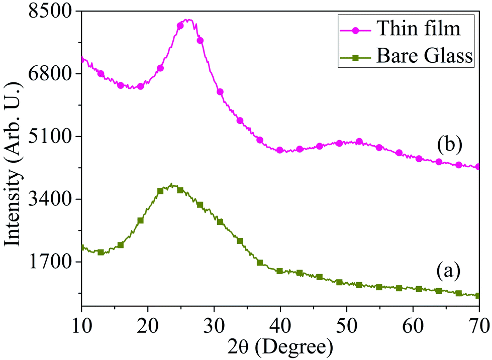
The synthesis procedure of MoOx QDs from bulk molybdenum oxide powder is shown schematically in Fig. 1. Thermally deposited MoOx layers are etching slowly into small particles. These particles further fragmented to even more small particles by ultra-sonication, which lead to the formation of well dispersed MoOx QDs. The MoOx thin films are deposited on glass substrate at 6 cm source-substrate distance and room temperature. The XRD spectrum of bare glass and thermally deposited MoOx thin film are shown in Fig. 2.
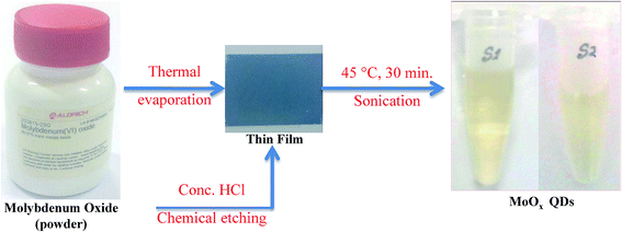 |
| | Fig. 1 Schematic representation of synthesis of MoOx QDs from bulk molybdenum oxide powder. | |
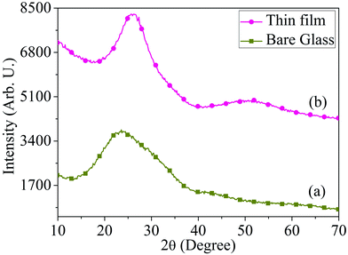 |
| | Fig. 2 XRD spectrum of (a) bare glass and (b) thermally deposited MoOx thin film, respectively. | |
The broad XRD peak ranging from 2θ ∼20° to 30° is observed in the MoOx film due to the glass substrate only. No significant XRD peaks are observed in the MoOx film. This may be attributed to the low mobility of evaporated atoms on the substrate surface and less interaction between the molybdenum and oxygen since this film is deposited at room temperature.39 Similar thin film samples are prepared under same deposition parameters that are subjected to chemical etching process for synthesis of QDs.
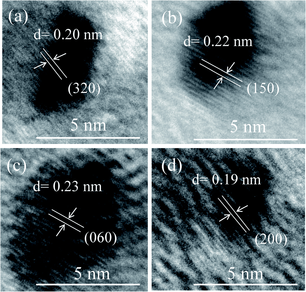
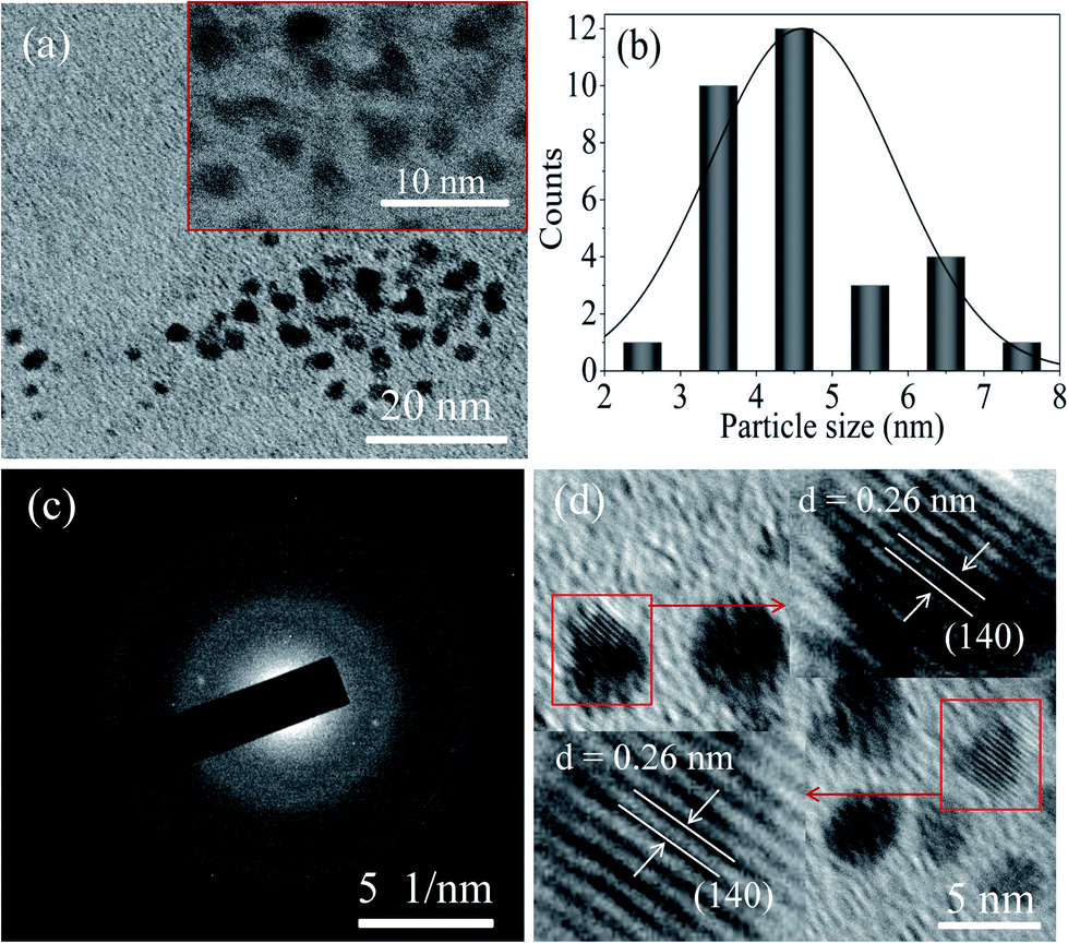
FETEM image analysis is carried out to investigate the size of the particles and crystallographic orientation of prepared QDs. FETEM image of the sample S1 is shown in Fig. 3(a). It confirmed the formation of nearly spherical shape of MoOx QDs of sample S1. The size distribution histogram gives the average size among thirty QDs is ∼4.3 nm, shown in Fig. 3(b) for the sample S1. The Fig. 3(c) shows the bright field image of corresponding SAED pattern. The SAED pattern revealed that QDs are polycrystalline in nature. There are two lattice planes each (218) and (420) corresponding to h-MoO3 phase (JCPDS: 21-0569) and that of (200) and (060) corresponding to α-MoO3 phase (JCPDS: 05-0508), respectively. The HRTEM images, Fig. 4(a)–(d) reveals that lattice spacing of QDs are ∼0.20 nm correspond to (320) lattice plane of h-MoO3 phase (JCPDS: 21-0569) and ∼0.22 nm, 0.23 nm and 0.19 nm correspond to (150), (060) and (200) lattice planes of α-MoO3 phase (JCPDS: 05-0508), respectively.
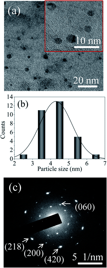 |
| | Fig. 3 (a) FETEM image of the sample S1 (inset magnified area), (b) the corresponding particle size distribution histogram, and (c) SAED pattern of MoOx QDs for the sample S1. | |
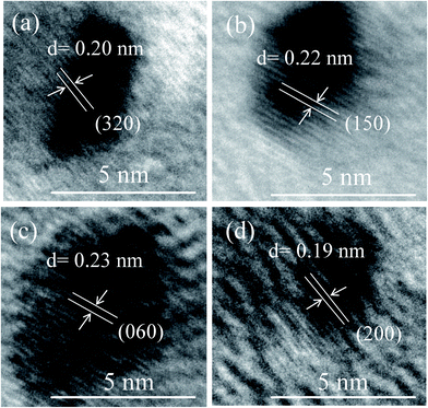 |
| | Fig. 4 (a–d) The HRTEM image of four different MoOx QDs of the sample S1. | |
Moreover, FETEM image confirmed the nearly spherical shape of MoOx QDs for the sample S2, as shown in Fig. 5(a)–(d). The size distribution histogram gives the average size ∼4.6 nm (Fig. 5(b)). The SAED pattern, Fig. 5(c), revealed that these QDs are also polycrystalline in nature. Highly ordered and parallel lattices in the HRTEM image, Fig. 5(d) of the QDs suggested its crystallization with lattice spacing ∼0.26 nm, which is associated with (140) lattice plane of α-MoO3 phase (JCPDS: 05-0508). For the samples: S1 and S2, the inter planner spacing along with crystal planes observed in HRTEM image and estimated from SAED pattern are listed in Table 1. These studies indicate that the small nano-crystals are QDs of MoO3. The bulk MoO3 powder can be transformed to the QDs with tuneable phase and size with the careful optimization of various parameters involved in this modified technique. In addition, by this modified technique amorphous MoOx thin film is successfully transformed into the polycrystalline QDs with co-existence of α-MoO3 and h-MoO3 phase, as confirmed by XRD and SAED patterns analysis. There are several reports on the synthesis of MoOx nano-materials in presence of surfactant.4,19,40 However, in the present work a well dispersed stable MoOx QDs are successfully synthesized without any surfactant. The observed polydispersity of the particle size distribution can be minimized with the use of suitable capping or stabilizing agent during the chemical etching process.
 |
| | Fig. 5 (a) FETEM image of the sample S2 (inset magnified area), (b) the corresponding particle size distribution histogram, (c) the SAED pattern of MoOx QDs, and (d) the HRTEM image of MoOx QDs for the sample S2. | |
Table 1 Estimated optical and structural parameters of MoOx QDs along with the sample codes
| Sample code |
Concentration of HCl acid (%) |
Band gap energy (eV) |
Average particle size (nm) |
Inter planner spacing, d (nm) |
(hkl) planes |
Phase assignment |
| S1 |
25 |
∼5.01 |
∼4.3 |
0.20 |
(320) |
h-MoO3 |
| 0.22 |
(150) |
h-MoO3 |
| 0.23 |
(060) |
α-MoO3 |
| 0.19 |
(200) |
α-MoO3 |
| S2 |
30 |
∼4.98 |
∼4.6 |
0.26 |
(140) |
α-MoO3 |
| 0.26 |
(140) |
α-MoO3 |
The increase of size of the particles with the increase of solution concentration (more than two sample concentration) were reported by H. S. Dehsari et al. and J. H. Huang et al.41,42 In the present investigation, similar increase in the size of QDs with the increase in HCl acid concentration in the sample solution is also observed. It is because, only few particles are available at the lower concentration of the solution and they tend to stay apart due to strong repulsive force. This reduces the growth rate due to less mass transfer in the reaction medium.41,42 However, at higher concentration the number density of the particles is increased which in turn reduced the inter-particle distances. There is a high mass transfer at low inter-particle distance and thereby causing the higher growth rate of the QDs.41,42 The QDs are synthesised at lower HCl acid concentration showed the co-existence of h-MoO3 and α-MoO3 phases. It is also observed that these mixed phase transformed to thermodynamically stable α-MoO3 phase with increase of HCl acid concentration from 25% to 30% in the solution. It is because, at lower concentration of HCl acid, only few H+ ions were adsorbed on the negative polar plane of growth unit of the MoO3 i.e., MoO6 octahedron. Thus, the corner to corner growth became the basis of the growth unit and it easily developed into a network shaped h-MoO3 phase.43 With the increase of HCl acid concentration in the sample solution, the concentration of H+ ion increased, which play a crucial role in MoO3 phase transformation. The growth rate of the negative polar plane of MoO6 octahedron is blocked, due to more and more H+ ions were adsorbed at the negative polar plane. Instead, the growth rate of the positive polar plane of MoO6 octahedron was far greater than others. Therefore, the growth is changed to superposition by sharing the edges and by sharing the corners of the positive polar plane structure, which developed into an α-MoO3 phase.43 In addition, the lower concentration of HCl acid will favour the formation of h-MoO3 phase.44
Spectral analysis
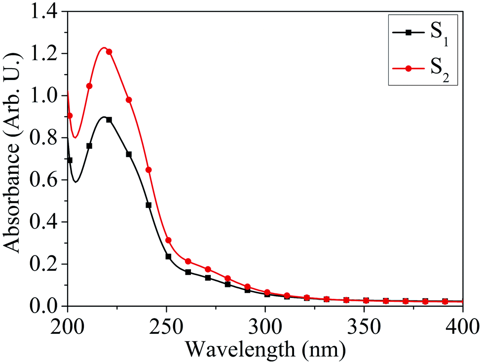
Absorption characteristics. The UV-Vis absorption spectra of MoOx QDs in the wavelength range, 200–400 nm for different concentration of HCl acid as shown in Fig. 6. The spectra confirm that the as-prepared MoOx QDs shows characteristic UV-Vis absorption peak at ∼219 nm and strong absorption between 200-300 nm. The strong absorption is due to the charge transfer of Mo–O band in the MoO66− octrahadron.40,45 The broadening of the absorption peak is ∼22 nm and ∼23 nm for the sample S1 and S2, respectively. The change in full width at half-maximum (FWHM) broadening with the change in HCl acid concentration 25% to 30% is observed to be marginal. The narrow FWHM data of QDs reflects their smaller particle size distribution.46,47 This is consistent with the present findings. The light yellow colour of the solution of MoOx QDs, as shown in Fig. 1, confirmed the formation of molybdenum trioxide (MoO3).26,48,49 The absence of distinct precipitation of the yellow solution indicates the fine disparity and stability of MoOx QDs. The absorbance is increased to ∼1.2 for sample S2 in comparison to that of S1, ∼0.9 along with bathchromic shift of ∼8 nm at the wavelength 230 nm. Higher HCl acid concentration in sample S2 produces more number of particles in the solution. This in turn led to the increase in absorbance. In addition, the red shift of absorption edge of sample S2 in comparison to that of S1 indicates the increase of particle size, which is in accordance with the result obtained from FETEM characterization. The optical band gaps (Eg) of QDs in the present work are estimated by using the eqn (1),50,51where, ‘B’ is the Tauc's slope, ‘hυ’ is the photon energy, ‘m’ is the transition probability. The value of ‘m’ is ½ for allowed transition in direct band gap material.50,51 The (αhυ)2–hυ plot for both sample: S1 and S2, as shown in Fig. 7. The optical band gap is estimated by linear extrapolation of the (αhυ)2–hυ plot. The calculated values of band gap are listed in Table 1. The optical band gap of the samples: S1 and S2 are ∼5.01 eV and 4.98 eV, respectively. The change is optical band gap is marginal with the present change in acid concentration. The band gap energy estimation shows there is blue shift for the MoOx QDs compared to that of bulk MoO3 (∼2.9 eV). This blue shift is due to the quantum confinement effect and hence, it reconfirmed the formation of QDs.52,53 The histogram of band gap and average particle size of MoOx QDs for different acid concentration is shown in Fig. 8.
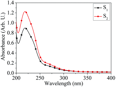 |
| | Fig. 6 UV-Vis absorption spectra of MoOx QDs for the samples: S1 and S2. | |
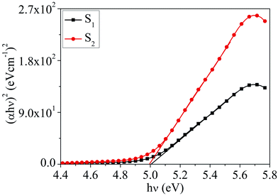 |
| | Fig. 7 The plot of (αhυ)2–hυ for the samples: S1 and S2. | |
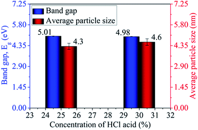 |
| | Fig. 8 Histogram of band gap and average particle size of MoOx QDs for different concentration of HCl acid. | |
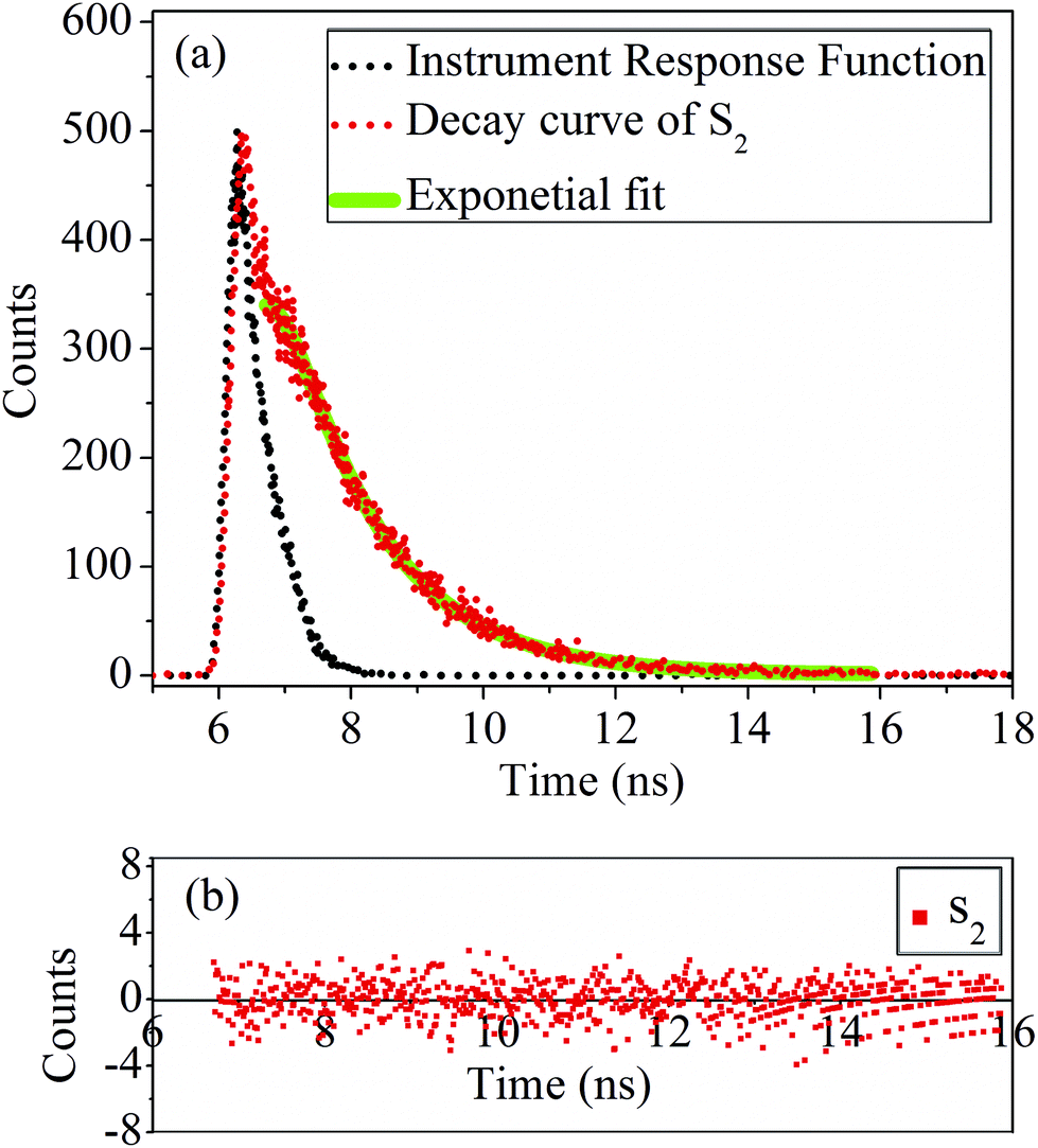
Photoluminescence (PL) characteristics. Time resolved PL was measured by a Life Spec-II, Edinburgh Instruments. The fluorescence decay curve of the sample S2 is shown in Fig. 9(a). The residual counts of the fluorescence decay curve is shown in Fig. 9(b). A 308 nm LED from Pico Quant was employed as the excitation source with a Hamamatsu Micro Channel Plate (MCP) as the detector. Using the FAST software provided by Edinburgh Instruments Ltd, the fluorescence decays were analysed by the reconvolution method. The goodness of fit is determined by the reduced chi-square (χ2) values and weighted residuals. The fluorescence decay of both the samples: S1 and S2 show lifetime of 1.40 and 1.42 ns, respectively and listed in Table 2. These results are quite indicative of the fact that the PL emissions of the QDs are fluorescent in nature. The fluorescence decay of the sample S1 and S2 show a single exponential decay as suggested by good χ2 values.
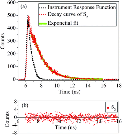 |
| | Fig. 9 (a) Fluorescence decay curve and (b) corresponding residual plot of the sample S2. | |
Table 2 Fluorescence lifetimes of MoOx QDs along with the sample codes
| Fluorophore |
Monitoring λmax |
Lifetime (ns) |
χ2 |
| S1 |
360 nm |
1.40 |
1.06 |
| S2 |
360 nm |
1.42 |
1.05 |
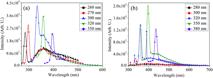
The PL spectra of MoOx QDs for the samples: S1 and S2 shown in Fig. 10(a) and (b), respectively. Similar to that of nanoparticles, MoOx QDs also exhibit excitation dependent PL behaviour. For the sample S1, PL spectra of MoOx QDs exhibit a strong emission peak at ∼360 nm under an excitation wavelength 300 nm. This fluorescence emission peak at ∼360 nm is due to the band to band transition and oxygen vacancies, Mo interstitial and surface defect of MoOx QDs. In addition, the emission peak at ∼363 nm is related to the indigo emission corresponding to the near band edge emission and it is close to the reported value of 365 nm.54,55 Similarly for the sample S2, the strong fluorescence emission peak appears at ∼410 nm upon excitation with 350 nm wavelength. As per crystal field model, the fluorescence emission peak at ∼410 nm may be attributed due to the Mo5+ dyz1–dxy1 band transition of a heavily distorted polyhedron (Mo–O) in a octahedral crystal field.52 The blue emission peaks at ∼420 and 400 nm are mostly related to the band to band transition with high Stokes shift.56–58 Digging more into this experiment, PL spectra for both the samples were recorded at various excitation wavelengths. In these PL spectra, a very weak shoulders along with the strong fluorescence emission peaks are detected for both samples under different excitation wavelengths. The weak shoulders are appeared due to the electron–hole recombination between the conduction band and the sublevel of adsorbed oxygen acceptors; which are disappeared with the increase in excitation wavelengths.59 The fluorescence emission peaks bathochromically shifted from ∼363 to 360 nm for the sample S1 with an increase in the excitation wavelength from 260 to 350 nm. The fluorescence intensity was observed to change with excitation wavelengths. Similar bathochromic shift from ∼420 to 410 nm was also observed for the sample S2 with the change in excitation wavelength from 280 to 380 nm. This phenomenon usually appears in QDs that derived from 2D materials.40,60–63 This is because of the inhomogeneity of chemical components and polydispersity of the lateral sizes,64 which is again in consistent with FETEM observation. This phenomenon mostly likely due to the distribution of emissive trap sites on the surface of MoOx QDs and quantum confinement effect.60
 |
| | Fig. 10 Excitation dependent PL spectra of MoOx QDs for the samples (a) S1 and (b) S2, respectively. | |
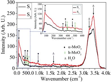
Micro-Raman characteristics. In order to further validate the existence of MoOx material, the Raman spectroscope is used. The micro-Raman spectra recorded in the wavenumber range, 50–4000 cm−1 for different HCl acid concentration is shown in Fig. 11. The micro-Raman peaks for α-MoO3 phase of the sample S1 and S2 are located at ∼89, 327, 952 cm−1, and 89, 370, 473, 952 cm−1, respectively.57,65,66 In addition, two Raman peaks of h-MoO3 phase are appeared at ∼398 and 492 cm−1 for the sample S1.67 The magnified area of the micro-Raman spectra in wavenumber range 50–600 cm−1 corresponding to the samples: S1 and S2 are shown in the inset of Fig. 11. Vibrational analysis by micro-Raman spectra reveals that the broad peaks around 1000–600 cm−1, 600–200 cm−1 and below 200 cm−1 are associated with Mo–O stretching, bending and lattice vibration mode, respectively.66,68 The sharp intense peak located ∼89 cm−1 is assigned to the rigid transitional vibration of MoO4 tetrahedral chain.65 The peaks at ∼327 and 370 cm−1 are assigned to O–Mo–O bending and scissoring vibrations.57 The characteristics Raman peaks of h-MoO3 phase at ∼398 and 492 cm−1 are assigned to O–Mo–O vibrational mode.67 The peak at ∼473 cm−1 corresponds to the Mo–O stretching and bending vibration of MoO6 octahedra.69 The presence of Mo6+ = O stretching vibration of terminal oxygen atoms is confirmed by the peak at ∼952 cm−1. These terminal oxygen bonds are created by breaking doubly coordinated oxygen (Mo2–O) bonds at the corner-shared oxygen, which are common to two octrahedra in the α-MoO3 phase.66 The QDs with mixed phase: α-MoO3 and h-MoO3 transformed to α-MoO3 phase with increase in HCl acid concentration from 25% to 30%. The micro-Raman peaks at ∼1645, 3250 and 3425 cm−1 are due to H2O scissor vibration and stretching vibration of the hydrogen-bonded OH groups.70
 |
| | Fig. 11 Micro-Raman spectra of MoOx QDs for the sample S1 and S2, respectively. | |
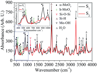
FTIR characteristics. The IR absorption spectra of the samples: S1 and S2 shown in Fig. 12, in the wavenumber range 400–4000 cm−1 are recorded for further study of vibrational properties of MoOx QDs. The samples show the absorption peak in the spectral range 400–1000 cm−1 corresponding to stretching and bending vibrations of metal–oxygen characteristics bonds.71 The characteristics absorption peaks for α-MoO3 phase of the sample S1 and S2 are located at ∼502, 648, 811, 901, 1002 cm−1 and ∼502, 512, 674, 811, 901, 1002 cm−1, respectively.11,24,40,55,72–74 In addition, two absorption peaks of h-MoO3 phase are appeared at ∼548 and 711 cm−1 for the sample S1.67 The magnified area of the FTIR absorption spectra in wavenumber range, 400–1040 cm−1 corresponding to the samples: S1 and S2 are shown in the inset of Fig. 12. The absorption peak located at ∼502 and 512 cm−1 are attributed to the bending mode of vibration of the Mo–O–Mo entity, while the O2− ion is shared by three Mo6+ ions.55,72 The absorption peaks of h-MoO3 phase are ∼548 and 711 cm−1, associated with the vibration of Mo–O and Mo–O–Mo bond, respectively.67 The peak at ∼648 cm−1 could be assigned to the stretching vibration of Mo–O–Mo.11 The absorption peak at ∼674 cm−1 is due to the triply coordinated oxygen (Mo3–O) stretching vibrational mode.40 A broad peak observed at ∼811 nm is due to the bridging vibration of Mo![[double bond, length as m-dash]](https://www.rsc.org/images/entities/char_e001.gif) O and indicated that the existence of Mo6+ oxidation state is related to the α-MoO3 phase.73 Two absorption peak located at ∼901 and 1002 cm−1, associated with the stretching vibration of MoO, which is the specification of terminal double bonds. This confirms the basic characterises of a layered structure of α-MoO3.24,74 The phase transformation of MoOx (x = 2, 3) QDs with the concentration of HCl acid is also confirmed by FTIR absorption spectra. The peak at ∼1157 cm−1 is due to Si–O–Si asymmetric vibration in longitudinal optical mode.75 In addition, three absorption peaks are observed at ∼1384, 1460 and 1643 cm−1, where first peak is attributed to vibrational mode of the Mo–OH bond and other two correspond to bending mode of Mo–OH, which assigned the presence of adsorbed free water molecules.59,76 Moreover, the absorption peaks at ∼1619, and 3574 cm−1 are assigned to the stretching and bending vibration of O–H bonds of adsorbed water molecules, respectively.77 The peak at ∼2110 cm−1 corresponds to the stretching vibration of Si–H in dehydrate groups at the silicon surface.78,79 The absorption peaks located at ∼2359, 3245 and 3492 cm−1 assigned to the H–O–H bending mode, symmetric and anti-symmetric O–H mode of water.67,80 The absorption peaks at ∼2809 and 3400 cm−1 are correspond to the typical O–H vibrations due to the adsorbed water molecule on the surface of MoOx QDs.40 The peak at ∼3737 cm−1 associated with the stretching vibration of O–H in silanol groups (Si–OH) isolated by the hydrogen bond.79 These FTIR results are consistent with the results obtained by HRTEM images and micro-Raman analysis.
O and indicated that the existence of Mo6+ oxidation state is related to the α-MoO3 phase.73 Two absorption peak located at ∼901 and 1002 cm−1, associated with the stretching vibration of MoO, which is the specification of terminal double bonds. This confirms the basic characterises of a layered structure of α-MoO3.24,74 The phase transformation of MoOx (x = 2, 3) QDs with the concentration of HCl acid is also confirmed by FTIR absorption spectra. The peak at ∼1157 cm−1 is due to Si–O–Si asymmetric vibration in longitudinal optical mode.75 In addition, three absorption peaks are observed at ∼1384, 1460 and 1643 cm−1, where first peak is attributed to vibrational mode of the Mo–OH bond and other two correspond to bending mode of Mo–OH, which assigned the presence of adsorbed free water molecules.59,76 Moreover, the absorption peaks at ∼1619, and 3574 cm−1 are assigned to the stretching and bending vibration of O–H bonds of adsorbed water molecules, respectively.77 The peak at ∼2110 cm−1 corresponds to the stretching vibration of Si–H in dehydrate groups at the silicon surface.78,79 The absorption peaks located at ∼2359, 3245 and 3492 cm−1 assigned to the H–O–H bending mode, symmetric and anti-symmetric O–H mode of water.67,80 The absorption peaks at ∼2809 and 3400 cm−1 are correspond to the typical O–H vibrations due to the adsorbed water molecule on the surface of MoOx QDs.40 The peak at ∼3737 cm−1 associated with the stretching vibration of O–H in silanol groups (Si–OH) isolated by the hydrogen bond.79 These FTIR results are consistent with the results obtained by HRTEM images and micro-Raman analysis.
 |
| | Fig. 12 FTIR absorption spectra of MoOx QDs for the sample S1 and S2, respectively. | |
Conclusions
In summary, this work developed a simple and modified top-down approach for synthesis of MoOx QDs. This process is a combination of thermal evaporation and sonication induced chemical etching to get the desired particles in the solution. The XRD analysis reveals the thermally deposited MoOx film is amorphous in nature. FETEM image analysis confirms the formation of spherical shaped MoOx QDs with an average size ∼4.3 and 4.6 nm. HRTEM, SAED, micro-Raman, and FTIR analysis reveals that as-prepared QDs exhibit polycrystalline in nature with co-existence of α-MoO3 and h-MoO3 phase. MoOx QDs exhibited excitation dependent fluorescence emission. The amorphous MoOx thin film is able to transformed into the polycrystalline nature by this modified top-down approach. The bulk MoO3 powder is successfully transformed to well-dispersed QDs via this modified top-down sonication induced chemical etching approach. Further, optimization of various parameters in this approach will lead to the development of tuneable crystal phase and size of the QDs. This work also confirms the successful synthesis of well-dispersed and stable QDs without any surfactants.
Conflicts of interest
The authors declare no competing financial interest.
Acknowledgements
This work is partially supported by the UGC-BSR research project no. F.30-10/2017(BSR) and DST FIST grant (project no. SR/FST/PSI-217/2016) to the Department of Physics, Dibrugarh University, Dibrugarh. The authors acknowledge the CIF, IIT Guwahati, India, for providing the FETEM, FTIR, and Laser micro-Raman facilities.
References
- H. Cheng, T. Kamegawa, K. Mori and H. Yamashita, Angew. Chem., 2014, 53, 2910–2914 CrossRef CAS PubMed.
- D. Hanlon, C. Backes, T. Higgins, M. Hughes, A. O. Neill, P. King, N. Mcevoy, G. Duesberg, B. Sanchez and H. Pettersson, Chem. Mater., 2014, 26, 1751–1763 CrossRef CAS.
- M. Ibrahem, F. Wu, D. Mengistie, C. Chang, L. Li and C. Chu, Nanoscale, 2014, 6, 5484–5490 RSC.
- B. Gao, H. Fan and X. Zhang, J. Phys. Chem. Solids, 2012, 73, 423–429 CrossRef CAS.
- L. Wang, X. Zhang, Y. Ma, M. Yang and Y. Qi, Mater. Lett., 2016, 164, 623–626 CrossRef CAS.
- B. Hu, L. Mai, W. Chen and F. Yang, ACS Nano, 2009, 3, 478–482 CrossRef CAS PubMed.
- J. Zhou, N. S. Xu, S. Z. Deng, J. Chen, J. C. She and Z. L. Wang, Adv. Mater., 2003, 15(21), 1835 CrossRef CAS.
- I. Shakir, M. Shahid, U. A. Rana and M. F. Warsi, RSC Adv., 2014, 4, 8741–8745 RSC.
- G. Wei, W. Qin, D. Zhang, G. Wang, R. Kim, K. Zheng and L. Wang, J. Alloys Compd., 2009, 481, 417–421 CrossRef CAS.
- M. Wang and K. J. Koski, ACS Nano, 2015, 9, 3226–3233 CrossRef CAS PubMed.
- G. Song, J. Shen, F. Jiang, R. Hu, W. Li, L. An, R. Zou, Z. Chen, Z. Qin and J. Hu, ACS Appl. Mater. Interfaces, 2014, 6, 3915–3922 CrossRef CAS PubMed.
- J. Yang, F. Lu, Y. Li, S. Yang, R. Li, N. Huo, C. Fan, Z. Wei, J. Li and S. S. Li, J. Mater. Chem. C, 2014, 2(6), 1034–1040 RSC.
- S. S. Sunu, E. Prabhu, V. Jayaraman, K. I. Gnanasekar and T. Gnanasekaran, Sens. Actuators, B, 2003, 94, 189–196 CrossRef CAS.
- F. J. Zhang, D. W. Zhao, Z. L. Zhuo, H. Wang, Z. Xu and Y. S. Wang, Sol. Energy Mater. Sol. Cells, 2010, 94, 2416–2421 CrossRef CAS.
- M. Y. Ameen, S. Pradhan, M. R. Suresh and V. S. Reddy, Opt. Mater., 2015, 39, 134–139 CrossRef.
- L. Zhou, L. Yang, P. Yuan, J. Zou, Y. Wu and C. Yu, J. Phys. Chem. C, 2010, 114, 21868–21872 CrossRef CAS.
- A. M. Hashem, H. Groult, A. Mauger, K. Zaghib and C. M. Julien, J. Power Sources, 2012, 219, 126–132 CrossRef CAS.
- S. Balendhran, S. Walia, M. Alsaif, E. P. Nguyen, J. Z. Ou, S. Zhuiykov, S. Sriram, M. Bhaskaran and K. Kalantar-zadeh, ACS Nano, 2013, 7, 9753–9760 CrossRef CAS PubMed.
- S. Bai, S. Chen, L. Chen, K. Zhang, R. Luo, D. Li and C. C. Liu, Sens. Actuators, B, 2012, 174, 51–58 CrossRef CAS.
- T. A. Tran, K. Krishnamoorthy, Y. W. Song, S. K. Cho and S. J. Kim, ACS Appl. Mater. Interfaces, 2014, 6, 2980–2986 CrossRef PubMed.
- K. Krishnamoorthy, M. Premanathan, M. Veerapandian and S. J. Kim, Nanotechnology, 2014, 25, 315101 CrossRef PubMed.
- X. Lu, R. Wang, F. Yang, W. Jiao, W. Liu, L. Hao and X. Hea, J. Mater. Chem. C, 2016, 4(28), 6720–6726 RSC.
- Y. Xu, X. Wang, W. L. Zhang, F. Lv and S. Guo, Chem. Soc. Rev., 2018, 47, 586–625 RSC.
- L. Yuan, Y. Niu, R. Li, L. Zheng, Y. Wang, M. Liu, G. Xu, L. Huang and Y. Xu, J. Mater. Chem. B, 2018, 6(20), 3240–3245 RSC.
- L. Zhang, M. F. Hong, Z. J. Chu, H. Xu, S. P. Wang, X. J. Zhao and S. J. Xiao, Microchem. J., 2018, 141, 170–175 CrossRef CAS.
- H. Zu, Y. Guo, H. Yang, D. Huang, Z. Liu, Y. Liu and C. Hu, New J. Chem., 2018, 42, 18533–18540 RSC.
- B. Li, X. Wang, X. Wu, G. He, R. Xu, X. Lu, F. R. Wang and I. P. Parkin, Nanoscale, 2017, 9(31), 11012–11016 RSC.
- T. T. P. Pham, P. H. D. Nguyen, T. T. Vo, H. H. P. Nguyen and C. L. Luu, Adv. Nat. Sci.: Nanosci. Nanotechnol., 2015, 6, 045010 Search PubMed.
- Q. Xu, W. Cai, W. Li, T. S. Sreeprasad, Z. He, W. J. Ong and N. Li, Mater. Today Energy, 2018, 10, 222–240 CrossRef.
- L. Niu, J. N. Coleman, H. Zhang, H. Shin, M. Chhowalla and Z. Zheng, Small, 2016, 12, 272–293 CrossRef CAS PubMed.
- X. Zhang, Z. Lai, Z. Liu, C. Tan, Y. Huang, B. Li, M. Zhao, L. Xie, W. Huang and H. Zhang, Angew. Chem., Int. Ed., 2015, 54(18), 5425–5428 CrossRef CAS PubMed.
- Y. P. Sun, B. Zhou, Y. Lin, W. Wang, K. A. S. Fernando, P. Pathak, M. J. Meziani, B. A. Harruff, X. Wang, H. Wang, P. G. Luo, H. Yang, M. E. Kose, B. Chen, L. M. Veca and S. Y. Xie, J. Am. Chem. Soc., 2006, 128, 7756–7757 CrossRef CAS PubMed.
- L. A. Ponomarenko, F. Schedin, M. I. Katsnelson, R. Yang, E. W. Hill, K. S. Novoselov and A. K. Geim, Science, 2008, 320, 356–358 CrossRef CAS PubMed.
- Q. Huang, S. Hu, J. Zhuang and X. Wang, Chem.–Eur. J., 2012, 18(48), 15283–15287 CrossRef CAS PubMed.
- S. Xu, D. Li and P. Wu, Adv. Funct. Mater., 2015, 25(7), 1127–1136 CrossRef CAS.
- D. Gopalakrishnan, D. Damien and M. M. Shaijumon, ACS Nano, 2014, 8(5), 5297–5303 CrossRef CAS PubMed.
- Z. Sun, H. Xie, S. Tang, X. F. Yu, Z. Guo, J. Shao, H. Zhang, H. Huang, H. Wang and P. K. Chu, Angew. Chem., Int. Ed., 2015, 11526–11530 CrossRef CAS PubMed.
- Z. Wu, D. Wang, X. Liang and A. Sun, Ultrason. Sonochem., 2011, 18, 288–292 CrossRef CAS PubMed.
- D. J. Borah, A. T. T. Mostako, P. K. Saikia and P. Dutta, Mater. Sci. Semicond. Process., 2019, 93, 111–122 CrossRef CAS.
- N. Wang, D. Tang, H. Zou, S. Jia, Z. Sun, X. Yang and J. Peng, Opt. Mater., 2018, 83, 19–27 CrossRef CAS.
- H. S. Dehsari, A. H. Ribeiro, B. Ersoz, W. Tremel, G. Jakob and K. Asadi, CrystEngComm, 2017, 19(44), 6694–6702 RSC.
- J. H. Huang, H. J. Parab, R. S. Liu, T. C. Lai, M. Hsiao, C. H. Chen, H. S. Sheu, J. M. Chen, D. P. Tsai and Y. K. Hwu, J. Phys. Chem. C, 2008, 112, 15684–15690 CrossRef CAS.
- L. Jiwen, W. Shizhong, Z. Guo-shang, X. Liujie, L. Wei and P. Kunming, Int. J. Electrochem. Sci., 2017, 12, 2429–2440 CrossRef.
- Y. P. Fang, A. W. Xu, A. M. Qin and R. J. Yu, Cryst. Growth Des., 2005, 5(3), 1212–1225 CrossRef.
- T. Xia, Q. Li, X. Liu, J. Meng and X. Cao, J. Phys. Chem. B, 2006, 110, 2006–2012 CrossRef CAS PubMed.
- Y. Zhang, H. Zhang, M. Ma, X. Guo and H. Wang, Appl. Surf. Sci., 2009, 255, 4747–4753 CrossRef CAS.
- C. M. Donega, S. G. Hickey, S. F. Wuister, D. Vanmaekelbergh and A. Meijerink, J. Phys. Chem. B, 2003, 107(2), 489–496 CrossRef.
- Y. Zhan, Y. Liu, H. Zu, Y. Guo, S. Wu, H. Yang, Z. Liu, B. Lei, J. Zhuang, X. Zhang, D. Huang and C. Hu, Nanoscale, 2018, 10(13), 5997–6004 RSC.
- I. A. Castro, R. S. Datta, J. Z. Ou, A. C. Gomez, S. Sriram, T. Daeneke and K. K. Zadeh, Adv. Mater., 2017, 29(40), 1701619 CrossRef PubMed.
- P. A. Arasu and R. V. Williams, J. Adv. Dielectr., 2017, 7, 1750011 CrossRef CAS.
- J. Tauc, Mater. Res. Bull., 1968, 3, 37–46 CrossRef CAS.
- I. Navas, R. Vinodkumar and V. P. M. Pillai, Appl. Phys. A, 2011, 103, 373–380 CrossRef CAS.
- S. Sapra and D. D. Sarma, Phys. Rev. B: Condens. Matter Mater. Phys., 2004, 69, 125304 CrossRef.
- A. H. Hammad and M. S. Abdel-wahab, Optik, 2018, 154, 777–784 CrossRef CAS.
- R. K. Sharma and G. B. Reddy, J. Alloys Compd., 2014, 598, 177–183 CrossRef CAS.
- A. Boukhachem, C. Bouzidi, R. Boughalmi, R. Ouerteni, M. Kahlaoui, B. Ouni, H. Elhouichet and M. Amlouk, Ceram. Int., 2014, 40, 13427–13435 CrossRef CAS.
- F. Chandoul, A. Boukhachem, F. Hosni, H. Moussa, M. S. Fayache, M. Amlouk and R. Schneider, Ceram. Int., 2018, 44(11), 12483–12490 CrossRef CAS.
- A. Boukhachem, M. Mokhtari, N. Benameur, A. Ziouche, M. Martínez, P. Petkova, M. Ghamnia, A. Cobo, M. Zergoug and M. Amlouk, Sens. Actuators, A, 2017, 253, 198–209 CrossRef CAS.
- A. Klinbumrung, T. Thongtem and S. Thongtem, J. Nanomater., 2012, 2012, 1–5 CrossRef.
- S. J. Xiao, X. J. Zhao, Z. J. Chu, H. Xu, G. Q. Liu, C. Z. Huang and L. Zhang, ACS Omega, 2017, 2(4), 1666–1671 CrossRef CAS PubMed.
- S. J. Xiao, X. J. Zhao, P. P. Hu, Z. J. Chu, C. Z. Huang and L. Zhang, ACS Appl. Mater. Interfaces, 2016, 8, 8184–8191 CrossRef CAS PubMed.
- S. J. Xiao, X. J. Zhao, J. Zuo, H. Q. Huang and L. Zhang, Anal. Chim. Acta, 2016, 906, 148–155 CrossRef CAS PubMed.
- X. Wang, G. Sun, N. Li and P. Chen, Chem. Soc. Rev., 2016, 45(8), 2239–2262 RSC.
- J. Zhang, Y. Pan, Y. Chen and H. Lu, J. Mater. Chem. C, 2018, 6(9), 2216–2220 RSC.
- M. Dieterle, G. Weinberg and G. Mestl, Phys. Chem. Chem. Phys., 2002, 4, 812–821 RSC.
- I. Navas, R. Vinodkumar, K. J. Lethy, A. P. Detty, V. Ganesan, V. Sathe and V. P. M. Pillai, J. Phys. D: Appl. Phys., 2009, 42, 175305 CrossRef.
- V. V. Atuchin, T. A. Gavrilova, V. G. Kostrovsky, L. D. Pokrovsky and I. B. Troitskaia, Inorg. Mater., 2008, 44, 622–627 CrossRef CAS.
- Y. Chen, C. Lu, L. Xu, Y. Ma, W. Hou and J. J. Zhu, CrystEngComm, 2010, 12, 3740–3747 RSC.
- Y. L. Xie, F. C. Cheong, Y. W. Zhu, B. Varghese, R. Tamang, A. A. Bettiol and C. H. Sow, J. Phys. Chem. C, 2010, 114, 120–124 CrossRef CAS.
- I. Pernoll, U. Maier, R. Janoschek and G. Zundel, J. Chem. Soc., Faraday Trans. 2, 1975, 71(10), 201–206 RSC.
- A. Chithambararaj and A. C. Bose, J. Alloys Compd., 2011, 509, 8105–8110 CrossRef CAS.
- J. Chen, M. Wang, X. Liao, Z. Liu, J. Zhang, L. Ding, L. Gao and Y. Li, J. Alloys Compd., 2015, 619, 406–410 CrossRef CAS.
- S. Subbarayudu, V. Madhavi and S. Uthanna, ISRN Condens. Matter Phys., 2013, 2013, 1–9 CrossRef.
- V. Nirupama, K. R. Gunasekhar, B. Sreedhar and S. Uthanna, Curr. Appl. Phys., 2010, 10, 272–278 CrossRef.
- R. A. Oweini and H. E. Rassy, J. Mol. Struct., 2009, 919, 140–145 CrossRef.
- R. K. Sharma and G. B. Reddy, Phys. B, 2015, 456, 197–205 CrossRef CAS.
- P. Wongkrua, T. Thongtem and S. Thongtem, J. Nanomater., 2013, 2013, 1–8 CrossRef.
- Y. J. Chabal, Surf. Sci., 1986, 168, 594–608 CrossRef CAS.
- A. G. Milekhin, C. Himcinschi, M. Friedrich, K. Hiller, M. Wiemer, T. Gessner, S. Schulze and D. R. T. Zhan, Semiconductors, 2006, 40, 1304–1313 CrossRef CAS.
- B. Gowtham, V. Ponnuswamy, G. Pradeesh, J. Chandrasekaran and D. Aradhana, J. Mater. Sci.: Mater. Electron., 2018, 29, 6835–6843 CrossRef CAS.
|
| This journal is © The Royal Society of Chemistry 2020 |
Click here to see how this site uses Cookies. View our privacy policy here. 
 Open Access Article
 This Open Access Article is licensed under a Creative Commons Attribution-Non Commercial 3.0 Unported Licence
 *a,
Angshuman Thunder Borgogoia,
Prasanta Kumar Saikiab and
Ashim Malakarc
*a,
Angshuman Thunder Borgogoia,
Prasanta Kumar Saikiab and
Ashim Malakarc