DOI:
10.1039/C9RA09186F
(Paper)
RSC Adv., 2020,
10, 2959-2966
Effect of silver doping on ultrafast broadband nonlinear optical responses in polycrystalline Ag-doped InSe nanofilms at near-infrared†
Received
6th November 2019
, Accepted 10th December 2019
First published on 15th January 2020
Abstract
There is great interest in transition metal-doped InSe because of its high nonlinearity and ultrafast response time at higher light fluence. Herein, Ag-doped InSe nanofilms were precisely manufactured using a direct current-radio frequency sputtering method, and their ultrafast broadband nonlinear optical responses in near-infrared were systematically researched. Ag-doped InSe nanofilm exhibited a broadband nonlinear optical response (800–1100 nm) and ultrafast carrier absorption (<1 ps), and can act as a potential semiconducting material for all-optical devices. Through precise control of the sputtering process parameters, Ag-doped InSe nanofilms were successfully prepared that were smooth, uniform, and exhibited no cracks. Nonlinear optical studies (femtosecond transient absorption spectroscopy and Z-scan measurement) indicated that nonlinear absorption behavior in Ag-doped InSe nanofilm withstands a transformation from saturation absorption to reverse saturation absorption arising from ground state bleaching, free-carrier absorption (FCA), and two-photon absorption (TPA). Additionally, nonlinear refraction behavior in Ag-doped InSe nanofilm was successfully detected near the intrinsic absorption edge, which arose from Kerr refraction and free-carrier refraction. More importantly, the broadband nonlinear response, ultrafast carrier absorption, and carrier recovery time of Ag-doped InSe nanofilm has the ability to controllably tune via Ag doping. Furthermore, Ag-doped InSe nanofilm possesses the nonlinear figure of merit (FOM) of 2.02, which indicates that Ag-doped InSe nanofilm is a promising semiconducting material for all-optical switching devices in near-infrared.
Introduction
It is well known that semiconducting materials exhibit unique nonlinear optical response features, including optical bistability, optical Kerr effect, and three-/four-wave mixing.1–3 The unique light-matter interactions in semiconducting materials represent an important step towards their wide-range application in optical bistable devices, interferometers, and optical oscillators.4–6 In the nonlinear optical domain, semiconducting materials have been found to exhibit nonlinear optical responses such as Kerr refraction and two-photon absorption (TPA), which can be extensively applied in optical switching, optical communication, and optical limiting.7–11 When the energy gap (Eg) and energy of incident photon (hν) meet the requirement (hν < Eg < 2hν), this leads to TPA behavior.12 When the nonlinear absorption is a TPA mechanism, Eg and hν meet the requirement (0.7 < hν/Eg < 1.0), leading to Kerr refraction behavior.13 Furthermore, the nonlinear absorption and refraction behaviour in semiconducting materials is also modulated by the photo-induced free-carrier effect.14 For instance, semiconducting materials such as GaN that exhibit TPA, free-carrier absorption (FCA), and Kerr refraction behaviour with large nonlinear absorption and refraction coefficients have been utilized in all-optical device applications.14 Nonetheless, many challenges in semiconducting materials still exist, such as the need for a broadband nonlinear optical response, ultrafast carrier absorption, higher nonlinear absorption coefficient, and nonlinear refraction index.
Recent experimental studies on InSe (III–VI group compound semiconductor) indicate that InSe exhibits excellent nonlinear optical responses that can be extensively applied in all-optical devices.15,16 To further enhance its nonlinear optical responses and widen its all-optical device applications, InSe is continually doped with transition metal elements.17–19 Multiple transition metal elements were selected to manufacture transition metal-doped InSe due to their robust optical properties that lead to promotion of their wide application in all-optical devices.20,21 Among the multiple transition metal elements, silver (Ag) from group IB can act as an excellent dopant for InSe because it can increase the excited absorption cross-section and effectively promote absorption in the excited state in near-infrared. With successful doping, Ag effectively modulated the energy gap and enhanced the TPA and FCA in InSe, which facilitated the movement of the nonlinear optical response band to broadband and established nonlinear refraction. A fundamental understanding of the ultrafast broadband nonlinear optical responses in Ag-doped InSe nanofilm and the Ag doping effect is necessary to engineer more optimal transition metal-doped InSe material for all-optical devices.
Herein, Ag-doped InSe and pure InSe nanofilms were precisely manufactured using a direct current-radio frequency sputtering technique. Ag-doped InSe nanofilm exhibits a broadband nonlinear optical response, ultrafast carrier absorption, higher nonlinear absorption coefficient, and nonlinear refraction index in near-infrared light, and the end product is a potential semiconducting material for all-optical devices. Through precise control of sputtering process parameters (such as sputtering temperature, reactant pressure, radio frequency power, deposition time, and shielding gas flow), a smooth, uniform nanofilm with no cracks and with a mean size of 30–40 nm was successfully prepared for Ag-doped InSe nanoparticles. Via femtosecond Z-scan and transient absorption spectroscopy measurements, it was found that the nonlinear absorption behaviour withstood a transformation from saturation absorption to reverse saturation absorption in Ag-doped InSe film at near-infrared wavelengths, which occurred due to ground state bleaching, TPA, and FCA. Additionally, Kerr refraction and free-carrier refraction behaviours were observed in Ag-doped InSe nanofilm because of the formidable TPA, FCA, and excitation wavelength proximity to the intrinsic absorption edge. The values of the effective nonlinear absorption coefficient and nonlinear refraction index in Ag-doped InSe nanofilm were calculated under 800 nm and 1100 nm excitation. The unique nonlinear optical response of the Ag-doped InSe nanofilm was observed to be dependent on the Ag doping effect.
Building on the ultrafast broadband nonlinear optical responses found in Ag-doped InSe nanofilm at near-infrared, a nonlinear figure of merit (FOM) was calculated under 800 nm and 1100 nm excitation, and can be extensively applied in all-optical switching devices in femtosecond pulse lasers. Worthy of special mention in this work, an Ag-doped InSe nanofilm successfully increased the FOM values compared to pure InSe nanofilm under the same excitation conditions in near-infrared wavelengths.
Experimental section
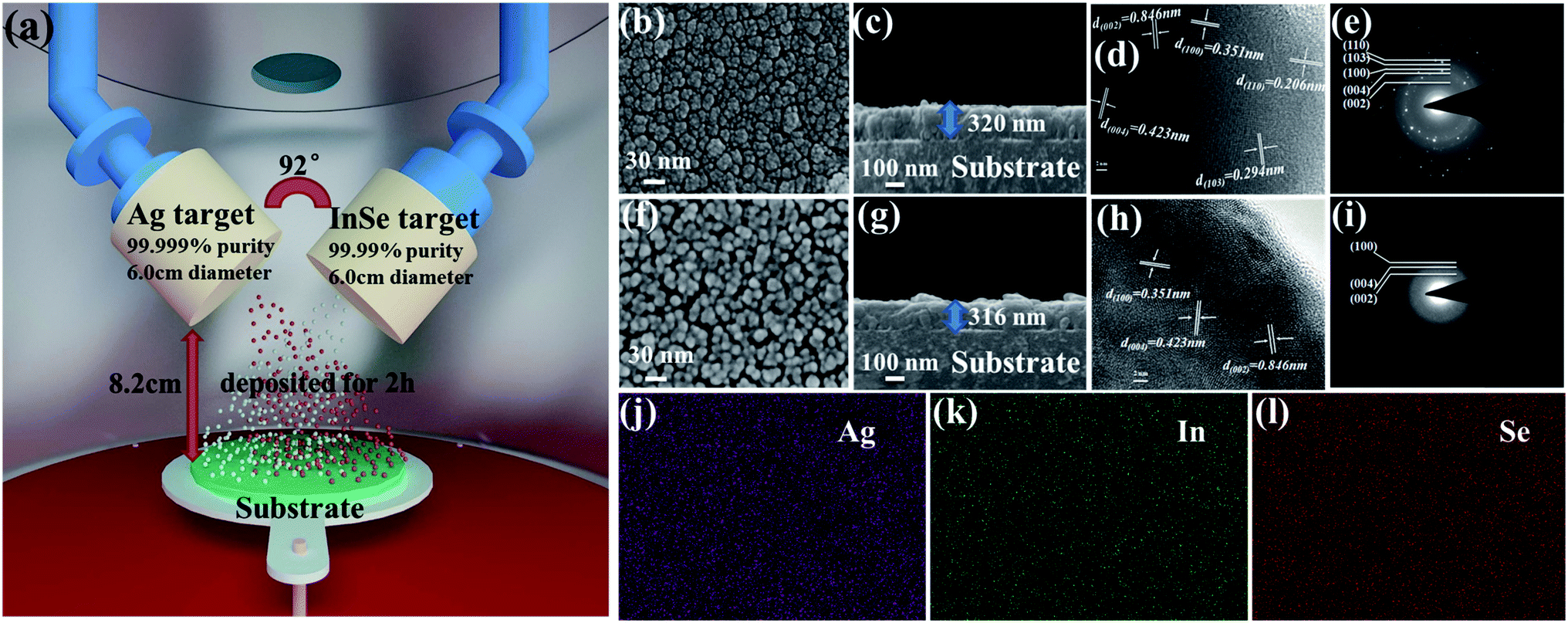
The Ag-doped InSe nanofilms were precisely manufactured on sapphire substrates using a direct current-radio frequency sputtering technique (Fig. 1a).22,23 The Ag-doped InSe and pure InSe nanofilms were examined by transmission electron microscopy (TEM) and scanning electron microscopy (SEM) to measure their thickness, composition, and structure (Fig. 1b–l). Compared with pure InSe nanofilm, the distribution of the Ag-doped InSe nanofilm tends to more smooth, uniform, and with no cracks. The mean size for Ag-doped InSe nanoparticles is 30–40 nm. In addition, cross-sectional SEM indicated that the Ag-doped InSe and pure InSe nanofilms are 320 and 316 nm thick, respectively.
 |
| | Fig. 1 (a) Illustration of direct current-radio frequency sputtering system setups for Ag-doped InSe nanofilm. (b) and (c) SEM micrographs of Ag-doped InSe nanofilm. (d) HRTEM micrograph of Ag-doped InSe nanofilm. (e) SAED pattern of Ag-doped InSe nanofilm. (f) and (g) SEM micrographs of pure InSe nanofilm. (h) HRTEM micrograph of pure InSe nanofilm. (i) SAED pattern of pure InSe nanofilm. (j–l) Elemental mapping images of Ag-doped InSe nanofilm. | |
High-resolution transmission electron microscopy (HRTEM) and selected area electron diffraction (SAED) from TEM observation are shown in Fig. 1(d, e, h and i), from where the lattice interplanar spacing is measured to be 0.846 nm, 0.423 nm, and 0.351 nm corresponding to the (002), (004), and (100) planes of hexagonal InSe, respectively. Furthermore, diffraction rings on the (103) and (110) planes for hexagonal InSe were also observed in the Ag-doped InSe nanofilm. The SAED pattern contained multiple diffraction rings, which demonstrate the polycrystalline nature of the hexagonal Ag-doped InSe product. Characterized by TEM micrograph, it was found that Ag doping does not affect the crystalline structure of InSe. According to the corresponding elemental mapping images (Fig. 1j–l), elemental Ag, In, and Se were equally dispersed throughout the entire Ag-doped InSe nanofilm.
The quantitative elemental analysis of Ag-doped InSe and pure InSe nanofilms included energy dispersive spectroscopy (EDS). Fig. 2a clearly shows that the concentration of incorporated Ag in the Ag-doped InSe nanofilm was 3.71%, and there are no peaks of impure elements from other materials. The linear absorption spectra of Ag-doped InSe and pure InSe nanofilms were characterized with a UV-Vis-NIR spectrophotometer, as shown in Fig. 2b. It is clearly seen that the intrinsic absorption edge of the Ag-doped InSe nanofilm exhibits a redshift compared with that of the pure InSe nanofilm. The reason for this phenomenon is that the density of states at the bottom of the conduction band is sparse, and the carrier caused by the Ag doping enters the conduction band, which leads to Moss–Burstein drift.24,25 The nonlinear optical response band may also exhibit shift dependence similar to that of linear absorption. For linear absorption, the following relational expression applies26
| |
 | (1) |
where
α denotes the absorption coefficient,
Eg denotes the energy gap,
C denotes a constant,
hν denotes the incident photon energy, and
n denotes an index (
n = 1, 2, 3…). The calculated values of the energy gap (
Eg) for Ag-doped InSe and pure InSe nanofilms were 1.75 and 1.89 eV, respectively.
 |
| | Fig. 2 (a) EDS image of Ag-doped InSe and pure InSe nanofilms. (b) Linear absorption spectrum of Ag-doped InSe and pure InSe nanofilms. The inset shows graphs of absorbance vs. photon energy. | |
Results and discussion
To further understand the mechanism governing nonlinear optical responses and evaluate the nonlinear refractive index and nonlinear absorption coefficient, femtosecond Z-scan measurements were obtained for Ag-doped InSe and pure InSe nanofilms (see Fig. 3 and 4).27,28 The excitation wavelength at 800 nm and 1100 nm was emitted from an optical parametric amplifier pumped by a Yb:KGW femtosecond laser (pulse width: 190 fs, repetition rate: 20 Hz, beam waist: 20 μm, and focal length of lens: 30 cm). The femtosecond open aperture Z-scan signals from the pure InSe nanofilm display reverse saturation absorption behavior under 800 nm excitation as shown in Fig. 3a, yet no signals were observed with excitation at 1100 nm in Fig. 3b. In consideration of the linear absorption spectrum results for pure InSe nanofilm in Fig. 2b, the reverse saturation absorption behavior of pure InSe nanofilm in femtosecond open aperture Z-scan measurement is ascribed to TPA effect. The induced absorption change can be expressed as29
 |
| | Fig. 3 (a) The femtosecond open aperture Z-scan data for pure InSe nanofilm detected at (a) 800 nm and (b) 1100 nm. The femtosecond open aperture Z-scan data for Ag-doped InSe nanofilm detected at (c) 800 nm and (d) 1100 nm. | |
 |
| | Fig. 4 The femtosecond closed aperture Z-scan signals of Ag-doped InSe nanofilm detected at (a) 800 nm and (b) 1100 nm. (c) The femtosecond closed aperture Z-scan signals of pure InSe nano film detected at 800 nm and 1100 nm. | |
where α denotes the entire absorption coefficient, I denotes the peak intensity of the incident laser, and α0 and β denote the linear and TPA coefficient, respectively. The fitting result in Fig. 3a shows that the TPA coefficient (β) with different peak intensities of incident laser under 800 nm excitation was evaluated as the same value (=210 cm GW−1).
It is well known that surface plasmon resonances in transition metal nanoparticles strongly enhance light-matter interactions.30 On this occasion, the robust plasmon-induced increase in the local electric field was found to enhance nonlinear optical responses by increasing the excited absorption cross-section.31 We tested the nonlinear optical responses of Ag-doped InSe nanofilm. The conversion behavior from saturation absorption to reverse saturation absorption at two different excitations (800 nm and 1100 nm) under different peak intensities of incident laser were measured as shown in Fig. 3c and d.
Saturation absorption behavior was observed across the 800 nm to 1100 nm range under low peak intensity of incident laser in femtosecond open aperture Z-scan measurement (Fig. 3c and d). Ag doping destroys the original lattice symmetry and forms the doping level, which boosts the optical absorption of ground state electrons. These electrons are promoted to the bottom of the conduction band in order to realize ground state bleaching, which generates saturation absorption behavior in Ag-doped InSe nanofilm.32 As the peak intensity of the incident laser increases, a tiny valley emerges on the original saturation absorption peak and becomes deeper. TPA and FCA are enhanced at high peak intensity of the incident laser due to reverse saturation absorption. As we discussed, there are two nonlinear absorption mechanisms with contrary signs in Ag-doped InSe nanofilm from 800 to 1100 nm. In order to interpret the nonlinear absorption behavior, we found a phenomenological model that is associated with reverse saturation absorption and saturation absorption. For the entire absorption coefficient, the following relational expression applies33
| |
 | (3) |
where
I denotes the peak intensity of the incident laser,
Is denotes the saturation peak intensity of the incident laser,
α denotes the entire absorption coefficient, and
α0 and
βeff denote the linear and effective nonlinear absorption coefficient, respectively. In
eqn (3), the first and second term describe the negative nonlinear absorption and positive nonlinear absorption, respectively. Moreover, the negative nonlinear absorption is caused by saturation absorption, while the positive nonlinear absorption is due to reverse saturation absorption. For an open aperture Z-scan, the normalized transmittance expression applies:
33| |
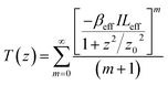 | (4) |
where
Leff = (1 − e
−α0L)/
α0,
Leff denotes the effective interaction length,
L denotes the thickness of the sample,
α0 and
βeff denote the linear and effective nonlinear absorption coefficient, respectively,
I denotes the peak intensity of the incident laser,
z denotes the distance from sample to focus (
z = 0), and
z0 denotes the diffraction length of the beam. The nonlinear optical absorption of Ag-doped InSe nanofilm is precisely fitted with the phenomenological model, as shown in
Fig. 3c and d. The effective nonlinear absorption coefficients (
βeff) of Ag-doped InSe nanofilm were found to be linearly enhanced with increasing peak intensity of the incident laser, and the values of
βeff at two excitation wavelengths (800 nm and 1100 nm) are presented in
Table 1.
Table 1 Summary of fitting parameters for a femtosecond Z-scan in Ag-doped InSe nanofilm at different peak intensities of incident laser and excitation
| Wavelength (nm) |
I (GW cm−2) |
βeff (×102 cm GW−1) |
n2 (×10−2 cm2 GW−1) |
FOM |
| 800 |
25.6 |
−2.4 |
2.8 |
1.46 |
| 128 |
3.1 |
3.8 |
1.53 |
| 256 |
4.8 |
6.5 |
1.69 |
| 359 |
7.3 |
9.2 |
1.56 |
| 1100 |
10.4 |
−1.8 |
3.0 |
1.52 |
| 50.2 |
2.4 |
4.3 |
1.63 |
| 104 |
3.1 |
6.9 |
2.02 |
| 152 |
4.2 |
8.6 |
1.86 |
The femtosecond closed aperture Z-scan signals from Ag-doped InSe nanofilm under 800 nm and 1100 nm excitation display Kerr refraction behavior, as shown in Fig. 4a and b, yet no signals were detected when the pure InSe nanofilm was excited at 800 nm and 1100 nm, as shown in Fig. 4c. In consideration of the linear absorption spectrum results for the Ag-doped InSe nanofilm in Fig. 2b, the intrinsic absorption edge of the Ag-doped InSe nanofilm proximity to excitation wavelength (800 nm and 1100 nm) as a result of Ag doping reduces the energy gap of InSe. On this occasion, a strong systematic dispersion of the bound electronic nonlinearity (Kerr effect) appears near the intrinsic absorption edge, which eventually leads to the establishment of Kerr refraction and free-carrier refraction behaviors in Ag-doped InSe nanofilm at different peak intensities of incident laser under 800 nm and 1100 nm excitation.13 With the assumption of a Gaussian profile for the incident laser, the variation of the on-axis sample transmittance in far field is proportional to the phase shift34
| |
 | (5) |
where
Leff = (1 − e
−α0L)/
α0,
Leff denotes the effective interaction length,
L denotes the thickness of the sample,
α0 denotes the linear absorption coefficient,
I denotes the peak intensity of the incident laser,
λ denotes the excitation wavelength, and
n2 denotes the nonlinear refractive index. In the Kerr system, the nonlinear refractive index possesses the same radial profile as the peak intensity of the incident laser, and then, the difference between the normalized peak and valley transmittance (Δ
Tp–v) and the peak-to-valley separation in
z (Δ
Zp–v) is given by:
34| | |
ΔTp–v = 0.406Δ∅, ΔZp–v = 1.7z0
| (6) |
The values of n2 can be extracted from the fittings of the closed aperture Z-scan curves using eqn (5) and (6). In addition, the FOM of the Ag-doped InSe nanofilm under 800 nm and 1100 nm excitation was calculated, and it was used to measure their performance in all-optical switching applications. The values of FOM and n2 at two excitations (800 nm and 1100 nm) are presented in Table 1.
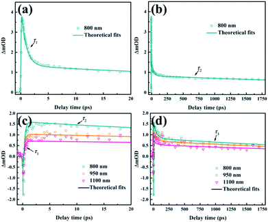
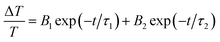
The transient absorption spectroscopy technique was used to characterize the nonlinear optical response of Ag-doped InSe and pure InSe nanofilms. The excitation wavelength at 620 nm was emitted from an optical parametric amplifier pumped by a Yb:KGW femtosecond laser with a pulse width of 190 femtoseconds. The typical pump fluence was <100 μJ cm−2. The probe pulses from the white-light supercontinuum (800–1100 nm) were generated by focusing 1030 nm laser pulses onto a YAG crystal [see Fig. 5 and 6].35,36 The alteration of absorption intensity at specific wavelengths obtained by the transient absorption spectra experiment is expressed by the optical density (ΔOD) variation. For the transient absorption spectra experiment, the optical density (ΔOD) is given by37
| | |
ΔOD(λp,t) = −log10(Ton/Toff)
| (7) |
where
t denotes the delay time,
λp denotes the wavelength of the probe beam,
Ton denotes the transmission of the probe beam with the pump beam, and
Toff denotes merely the transmission of the probe beam.
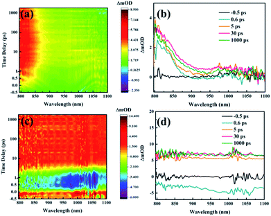 |
| | Fig. 5 (a) and (b) The transient absorption spectra of pure InSe nanofilm in the near-infrared region at 620 nm excitation. (c) and (d) The transient absorption spectra of Ag-doped InSe nanofilm in the near-infrared region at 620 nm excitation. | |
 |
| | Fig. 6 (a) and (b) The transient absorption curves of pure InSe nanofilm under disparate timescales at 620 nm excitation. (c) and (d) The transient absorption curves of Ag-doped InSe film under disparate timescales at 620 nm excitation. | |
The transient absorption spectra signals from pure InSe nanofilm under 800–875 nm excitation display reverse saturation absorption (ΔOD > 0) as shown in Fig. 5a and b, yet no signals were detected at other probe spectral regions. At 0.25 ps delay time, a Drude-like free carrier response in pure InSe nanofilm was observed, synchronously with a reverse saturation absorption signal (ΔOD > 0) almost straightway centered at 820 nm after excitation.38 During the entire delay time, the signal peak in the transient absorption spectra did not significantly move, indicating that the reverse saturation absorption may originate from the identical excited state energy level.16 It can be seen from the experimental result of the transient absorption spectra in Fig. 5c and d that the Ag-doped InSe nanofilm withstands a transformation from saturation absorption to reverse saturation absorption with a broadband nonlinear response (800–1100 nm). After photoexcitation, a bleaching peak appears at 1000 nm (ΔOD < 0). As the delay time increases, the bleaching peak broadens and then completely disappears within several picoseconds. In the wake of delay time increases, the reverse saturation absorption signal (ΔOD > 0) covered all the probing wavelengths, maintaining a broadband transient absorption spectrum that continued to several nanoseconds.39
It should also be noted that the sapphire substrate has no transient absorption signal under the same photon excitation. Consequently, the influence of substrate effect on the transient absorption experiment can be eliminated. We confirmed that the transient absorption signal is repeatable at different spots on Ag-doped InSe and pure InSe nanofilms, indicating that the uniformity of nanofilms is superior, and no photo-induced damage of the nanofilms was observed during our transient absorption experiment. Compared with pure InSe nanofilm, the transient absorption of Ag-doped InSe nanofilm has obvious advantages in broadband nonlinear response, ultrafast carrier absorption, nonlinear absorption intensity, and complicated absorption mechanisms.
The transient absorption curves of the pure InSe and Ag-doped InSe nanofilms under disparate timescales at 620 nm excitation are shown in Fig. 6. The results of the transient absorption experiment show that the pump beam effect does not influence the carrier recovery during the entire decay time, which manifests as the transient absorption experiments being implemented at low destabilization condition. Via global analysis, the transient absorption curves showing the entire delay time in pure InSe and Al-doped InSe nanofilms were fitted by double and triple exponential functions. For carrier recovery time, the following relational expression applies:40
| |
 | (8) |
| |
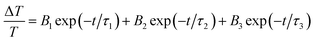 | (9) |
where
B1,
B2, and
B3 denote the amplitudes of the first, second, and third components, respectively. The values for the carrier recovery time in pure InSe nanofilm at 620 nm excitation were calculated as 1.71 ± 0.26 ps (
τ1) and 3.25 ± 0.24 ns (
τ2). The values for the carrier recovery time in Ag-doped InSe nanofilm at 620 nm excitation were calculated as 1.62 ± 0.25 ps (
τ1), 12.72 ± 0.79 ps (
τ2), and 3.13 ± 0.15 ns (
τ3). A schematic diagram of carrier recovery time is shown in
Fig. 7. The first carrier recovery time (
τ1) of pure InSe nanofilm is attributed to the cooling of thermal carriers with femtosecond optical pulses. The second carrier recovery time (
τ2) of pure InSe nanofilm is ascribed to the recovery of non-radiation transition for carriers from the bottom of the conduction band to the top of the valence band. The first carrier recovery time (
τ1) of Ag-doped InSe nanofilm is attributed to the cooling of thermal carriers, which is implemented by carrier-phonon interactions after the carriers are excited in the Ag-doped InSe nanofilm with femtosecond optical pulses. The second carrier recovery time (
τ2) is ascribed to the recovery of non-radiation transition for carriers from the bottom of the conduction band relaxation to the doping level. The third carrier recovery time (
τ3) is ascribed to the carrier lifetime from the bottom of the doping level to the top of the valence band.
 |
| | Fig. 7 (a) Illustration of pure InSe nanofilm band and carrier recombination process. (b) Illustration of Ag-doped InSe nanofilm band and carrier recombination process. | |
Conclusions
In summary, this work confirms TPA, FCA, Kerr refraction, and free-carrier refraction enhancement in nonlinear optical response at near-infrared as the dominating mechanism for nonlinear absorption and refraction in Ag-doped InSe nanofilm manufactured by a direct current-radio frequency sputtering technique. This research revealed the following excellent features of nonlinear optical response in Ag-doped InSe nanofilm: (i) Ag-doped InSe nanofilm exhibited a significantly broadband nonlinear response (800–1100 nm) that is useful for broadband all-optical devices in near-infrared, (ii) the broadband nonlinear response, ultrafast carrier absorption, carrier recovery time, high nonlinear absorption coefficient, and nonlinear refraction index of Ag-doped InSe nanofilm were observed to be dependent on the Ag doping, (iii) Ag-doped InSe nanofilm successfully increased the values of FOM compared to pure InSe nanofilm under the same excitation conditions in near-infrared. Lastly, the ultrafast broadband nonlinear optical responses in Ag-doped InSe nanofilm lead to the possibility of fabricating all-optical switching at near-infrared.
Conflicts of interest
The authors declare no competing financial interests.
Acknowledgements
This work is supported by grants from the National Natural Science Foundation of China (21371040, 11804244, and 21571042), and the Natural Science Foundation of Jiangsu Province (BK20180965 and BK20170375).
Notes and references
- J. B. Li, N. C. Kim, M. T. Cheng, L. Zhou, Z. H. Hao and Q. Q. Wang, Optical bistability and nonlinearity of coherently coupled exciton-plasmon systems, Opt. Express, 2012, 20(2), 1856–1861 CrossRef PubMed.
- W. K. Tse and A. H. Macdonald, Giant magneto-optical Kerr effect and universal Faraday effect in thin-film topological insulators, Phys. Rev. Lett., 2010, 105(5), 057401 CrossRef PubMed.
- M. Schmitt, G. Knopp, A. Materny and W. Kiefer, The Application of Femtosecond Time-Resolved Coherent Anti-Stokes Raman Scattering for the Investigation of Ground and Excited State Molecular Dynamics of Molecules in the Gas Phase, J. Phys. Chem. A, 2014, 102(23), 985–990 Search PubMed.
- Q. M. Ngo, S. Kim, S. H. Song and R. Magnusson, Optical bistable devices based on guided-mode resonance in slab waveguide gratings, Opt. Express, 2009, 17(26), 23459–23467 CrossRef CAS PubMed.
- I. Zanette, T. Weitkamp, T. Donath, S. Rutishauser and C. David, Two-Dimensional X-Ray Grating Interferometer, Phys. Rev. Lett., 2010, 105(24), 248102–248110 CrossRef PubMed.
- L. Razzari, D. Duchesne, M. Ferrera, R. Morandotti, S. Chu, B. E. Little and D. J. Moss, CMOS-compatible integrated optical hyper-parametric oscillator, Nat. Photonics, 2009, 4(1), 41–45 CrossRef.
- M. Drobizhev, N. S. Makarov, S. E. Tillo, T. E. Hughes and A. Rebane, Two-photon absorption properties of fluorescent proteins, Nat. Methods, 2011, 8(5), 393–399 CrossRef CAS PubMed.
- W. K. Tse and A. H. Macdonald, Giant Kerr Effect and Universal Faraday Effect in Thin-film Topological Insulators, Phys. Rev. Lett., 2010, 105(5), 057401 CrossRef PubMed.
- T. Volz, A. Reinhard, M. Winger, A. Badolato, K. J. Hennessy, E. L. Hu and A. Imamoglu, Ultrafast all-optical switching by single photons, Nat. Photonics, 2012, 6(9), 607–611 CrossRef CAS.
- I. B. Djordjevic and M. Arabaci, LDPC-coded orbital angular momentum (OAM) modulation for free-space optical communication, Opt. Express, 2010, 18(24), 24722–24728 CrossRef PubMed.
- J. D. Jia, X. Z. Wu, Y. Fang, J. Y. Yang, X. Guo, Q. Y. Xu, Y. B. Han and Y. L. Song, Ultrafast Broad-Band Optical Limiting in Simple Hydrazone Derivatives with a Π-Conjugated System: Effect of Two-Photon-Induced Singlet-State Absorption, J. Phys. Chem. C, 2018, 122(28), 16234–16241 CrossRef CAS.
- H. Chen and A. W. Poon, Two-photon absorption photocurrent in p-i-n diode embedded silicon microdisk resonators, Appl. Phys. Lett., 2010, 96(19), 191106 CrossRef.
- M. Sheik-Bahae, D. C. Hutchings, D. J. Hagan and E. W. Van Stryland, Dispersion of bound electron nonlinear refraction in solids, IEEE J. Quantum Electron., 1991, 27(6), 0–1309 CrossRef CAS.
- Y. Fang, F. Zhou, J. Y. Yang, X. Z. Wu, Z. G. Xiao, Z. G. Li and Y. L. Song, Anisotropy of two-photon absorption and free-carrier effect in nonpolar GaN, Appl. Phys. Lett., 2015, 106(13), 131903 CrossRef.
- N. Kuroda, O. Ueno and Y. Nishina, Supernonlinear Shifts of Optical Energy Gaps in InSe and GaSe under Hydrostatic Pressure, J. Phys. Soc. Jpn., 1986, 55(2), 581–589 CrossRef CAS.
- X. Y. Yan, X. Z. Wu, Y. Fang, S. R. Zhang, W. Y. Cheng, C. B. Yao, Y. X. Wang, X. R. Zhang and Y. L. Song, Morphological and nonlinear optical properties of Al:InSe thin films, Opt. Mater. Express, 2019, 9(7), 2955–2963 CrossRef.
- M. Kundakçi, B. Gürbulak, S. Doğan, A. Ateş and M. Yildirim, Urbach tail and electric field influence on optical properties of InSe and InSe:Er single crystals, Appl. Phys. A, 2008, 90(3), 479–485 CrossRef.
- O. Icelli, S. Erzeneoglu and B. Gurbulak, Mass attenuation coefficients for n-type InSe, InSe:Gd, InSe:Ho and InSe:Er single crystals, J. Quant. Spectrosc. Radiat. Transfer, 2005, 90(3–4), 399–407 CrossRef CAS.
- S. Shigetomi, T. Ikari, Y. Koga and S. Shigetomi, Photoconductivity and Photo-Hall Effect of p-Type InSe Single Crystals, Jpn. J. Appl. Phys., 1981, 20(5), L343–L346 CrossRef CAS.
- A. Ateş, M. Yıldırım and B. Gürbulak, Investigation of the electrical properties of Ho-doped InSe single crystal, Phys. E, 2004, 21(1), 85–90 CrossRef.
- S. Shigetomi and T. Ikari, Electrical and optical properties of n- and p-InSe doped with Sn and As, J. Appl. Phys., 2003, 93(4), 2301 CrossRef CAS.
- J. A. Jansen, J. G. Wolke, S. Swann, V. D. Jp and G. K. De, Application of magnetron sputtering for producing ceramic coatings on implant materials, Clin. Oral Implant. Res., 2010, 4(1), 28–34 CrossRef PubMed.
- S. H. Jeong, B. S. Kim and B. T. Lee, Photoluminescence dependence of ZnO films grown on Si(100) by radio-frequency magnetron sputtering on the growth ambient, Appl. Phys. Lett., 2003, 82(16), 2625–2627 CrossRef CAS.
- J. Dong and D. A. Drabold, Atomistic Structure of Band-Tail States in Amorphous Silicon, Phys. Rev. Lett., 1998, 80(9), 1928–1931 CrossRef CAS.
- W. S. Whitney, M. C. Sherrott, D. Jariwala, W. H. Lin, H. A. Bechtel, G. R. Rossman and H. A. Atwater, Field Effect Optoelectronic Modulation of Quantum-Confined Carriers in Black Phosphorus, Nano Lett., 2017, 17(1), 78–84 CrossRef CAS PubMed.
- H. Takeuchi, Enhancement effects on excitonic photoluminescence intensity originating from misaligned crystal blocks and polycrystalline grains in a ZnO wafer, Eur. Phys. J. B, 2013, 86(2), 1–5 CrossRef.
- M. Samoc, A. Samoc, B. Lutherdavies, Z. Bao, L. Yu, B. Hsieh and U. Scherf, Femtosecond Z-scan and degenerate four-wave mixing measurements of real and imaginary parts of the third-order nonlinearity of soluble conjugated polymers, J. Opt. Soc. Am. B, 1998, 15(2), 817–825 CrossRef CAS.
- Y. H. Lee, Y. Yan, L. Polavarapu and Q. H. Xu, Nonlinear optical switching behavior of au nanocubes and nano-octahedra investigated by femtosecond z-scan measurements, Appl. Phys. Lett., 2009, 95(2), 5233 Search PubMed.
- A. A. Said, M. Sheik-Bahae, D. J. Hagan, T. H. Wei, J. Wang, J. Young and E. W. Van Stryland, Determination of bound-electronic and free-carrier nonlinearities in ZnSe, GaAs, CdTe, and ZnTe, J. Opt. Soc. Am. B, 1992, 9(3), 405–414 CrossRef CAS.
- P. Vasa and C. Lienau, Strong Light–Matter Interaction in Quantum Emitter/Metal Hybrid Nanostructures, ACS Photonics, 2017, 5(1), 2–23 CrossRef.
- Y. Dong, S. Chertopalov, K. Maleski, B. Anasori, L. Hu, S. Bhattacharya, A. M. Rao, Y. Gogotsi, V. N. Mochalin and R. Podila, Saturable absorption in 2D Ti3C2 mxene thin films for passive photonic diodes, Adv. Mater., 2018, 30(10), 1705714 CrossRef PubMed.
- L. R. Hart, S. Li, C. Sturgess, R. Wildman, J. R. Jones and W. Hayes, 3D Printing of Biocompatible Supramolecular Polymers and their Composites, ACS Appl. Mater. Interfaces, 2016, 8, 3115–3122 CrossRef CAS PubMed.
- Y. Gao, X. Zhang, Y. Li, H. Liu, Y. Wang, Q. Chang, W. Y. Jiao and Y. L. Song, Saturable absorption and reverse saturable absorption in platinum nanoparticles, Opt. Commun., 2005, 251(4–6), 429–433 CrossRef CAS.
- M. Sheik-Bahae, A. A. Said, T. H. Wei, D. J. Hagan and E. W. Van Stryland, Sensitive measurement of optical nonlinearities using a single beam, IEEE J. Quantum Electron., 1990, 26(4), 760–769 CrossRef CAS.
- S. Chen, M. J. Bell, A. R. Beck, H. Mashiko, M. Wu, A. N. Pfeiffer, M. B. Gaarde, D. M. Neumark, S. R. Leone and K. J. Schafer, Light-induced states in attosecond transient absorption spectra of laser-dressed helium, Phys. Rev. A, 2012, 86(86), 29131–29136 Search PubMed.
- A. Grabowska, A. Mordziński, K. Kownacki, E. Gilabert and C. Rulličre, Picosecond transient-absorption and gain spectra of the excited internally hydrogen bonded benzoxazole derivatives: experimental proof of the thermal activation of the intramolecular proton transfer, Chem. Phys. Lett., 2017, 177(1), 17–22 CrossRef.
- Z. G. Li, R. Zhao, W. W. Li, H. Y. Wang, H. Yang and Y. L. Song, Strain dependent ultrafast carrier dynamics in EuTiO3 films, Appl. Phys. Lett., 2014, 105(16), 162904 CrossRef.
- D. Chekulaev, V. Garber and A. Kaplan, Free carrier plasma optical response and dynamics in strongly pumped silicon nanopillars, J. Appl. Phys., 2013, 113(14), 3249 CrossRef.
- S. D. Conte, M. Conforti, D. Petti, E. Albisetti, S. Longhi, R. Bertacco, C. D. Angelis, G. Cerullo and G. D. Valle, Disentangling electrons and lattice nonlinear optical response in metal-dielectric Bragg filters, Phys. Rev. B: Condens. Matter Mater. Phys., 2014, 89(12), 991–1000 Search PubMed.
- Y. Fang, J. Y. Yang, Z. G. Xiao, J. Y. Zhang, Y. Q. Chen, Q. Y. Wu and Y. L. Song, Ultrafast all-optical modulation in Fe-doped GaN at 1.31 and 1.55 μm with high contrast and ultralow power, Appl. Phys. Lett., 2017, 110, 161902 CrossRef.
Footnote |
| † Electronic supplementary information (ESI) available. See DOI: 10.1039/c9ra09186f |
|
| This journal is © The Royal Society of Chemistry 2020 |
Click here to see how this site uses Cookies. View our privacy policy here. 
 Open Access Article
 This Open Access Article is licensed under a Creative Commons Attribution-Non Commercial 3.0 Unported Licence
 a,
Xingzhi Wub,
Yu Fangb,
Wenjun Sunc,
Chengbao Yao
a,
Xingzhi Wub,
Yu Fangb,
Wenjun Sunc,
Chengbao Yao