
 Open Access Article
 This Open Access Article is licensed under a
 Creative Commons Attribution 3.0 Unported Licence
Computational insights into structural, electronic and optical characteristics of GeC/C2N van der Waals heterostructures: effects of strain engineering and electric field
Hong T. T. Nguyenab,
Tuan V. Vu ab,
Van Thinh Phamc,
Nguyen N. Hieud,
Huynh V. Phuce,
Bui D. Hoif,
Nguyen T. T. Binh*d,
M. Idreesg,
B. Aminh and
Chuong V. Nguyen*i
ab,
Van Thinh Phamc,
Nguyen N. Hieud,
Huynh V. Phuce,
Bui D. Hoif,
Nguyen T. T. Binh*d,
M. Idreesg,
B. Aminh and
Chuong V. Nguyen*i
aDivision of Computational Physics, Institute for Computational Science, Ton Duc Thang University, Ho Chi Minh City, Vietnam. E-mail: nguyenthithamhong@tdtu.edu.vn
bFaculty of Electrical & Electronics Engineering, Ton Duc Thang University, Ho Chi Minh City, Vietnam
cCenter of Excellence for Green Energy and Environmental Nanomaterials, Nguyen Tat Thanh University, Ho Chi Minh City, Vietnam
dInstitute of Research and Development, Duy Tan University, Da Nang 550000, Vietnam. E-mail: nguyentthanhbinh8@duytan.edu.vn
eDivision of Theoretical Physics, Dong Thap University, Cao Lanh 870000, Vietnam
fDepartment of Physics, University of Education, Hue University, Hue, Vietnam
gDepartment of Physics, Hazara University, Mansehra 21300, Pakistan
hDepartment of Physics, Abbottabad University of Science and Technology, Abbottabad 22010, Pakistan
iDepartment of Materials Science and Engineering, Le Quy Don Technical University, Ha Noi 100000, Vietnam. E-mail: chuongnguyen11@gmail.com
First published on 16th January 2020
Abstract
Vertical heterostructures from two or more than two two-dimensional materials are recently considered as an effective tool for tuning the electronic properties of materials and for designing future high-performance nanodevices. Here, using first principles calculations, we propose a GeC/C2N van der Waals heterostructure and investigate its electronic and optical properties. We demonstrate that the intrinsic electronic properties of both GeC and C2N monolayers are quite preserved in GeC/C2N HTS owing to the weak forces. At the equilibrium configuration, GeC/C2N HTS forms the type-II band alignment with an indirect band gap of 0.42 eV, which can be considered to improve the effective separation of electrons and holes. Besides, GeC/C2N vdW-HTS exhibits strong absorption in both visible and near ultra-violet regions with an intensity of 105 cm−1. The electronic properties of GeC/C2N HTS can be tuned by applying an electric field and vertical strains. The semiconductor to metal transition can be achieved in GeC/C2N HTS in the case when the positive electric field of +0.3 V Å−1 or the tensile vertical strain of −0.9 Å is applied. These findings demonstrate that GeC/C2N HTS can be used to design future high-performance multifunctional devices.
1. Introduction
Vertical heterostructures (HTSs) that are made layer-by-layer from two or more than two two-dimensional materials (2D) are recently considered as an effective tool for tuning the electronic properties of 2D materials and for designing future high-performance nanodevices owing to their promising properties, which may not be present in the individual 2D materials.1 The most common routes to synthesize the van der Waals (vdW) HTSs in experiments are chemical vapor deposition (CVD)2,3 and mechanical transfer process.4,5 To date, there are several vdW-HTSs based on 2D materials that have been experimentally fabricated, including graphene/transition metal dichalcogenides (TMDs),6–8 TMDs/TMDs,9–11 TMDs/BSe,12 TMDs/Mg(OH)2,13 and TMDs/BP14 which become promising candidates for future nanodevices, such as field-effect transistors (FETs), and tunnel diodes. Moreover, vdW-HTSs based on 2D materials have been proposed and investigated theoretically, such as GeSe/phosphorene,15 C2N/InSe,16 BP/MoSSe,17 arsenene/GaS,18 Ca(OH)2/arsenene,19 ZrS2/HfS2.20 All the above-mentioned studies demonstrate that constructing two 2D materials into vdW-HTSs provides an effective tool to design novel electronic and optoelectronic materials with favorable properties and novel phenomena, which are acceptable for future high-performance devices.Recently, graphene-like GeC and C2N monolayers have been widely explored in different fields of optoelectronic and nanoelectronic applications owing to their extraordinary properties. For instance, the field-effect transistor based on C2N exhibits a high on/off ratio of 107.21 Additionally, C2N monolayer shows extremely high selectivity and large permeance in favor of H2, which can be used for hydrogen separation.22 Monolayer C2N was obtained in experiments from a bottom-up wet–chemical reaction.21 Whereas, 2D GeC exhibits a dynamically stable planar structure and demonstrates excellent electronic and optical properties,23,24 high thermal conductivity,25 which make it potential material for electronic, optoelectronic, and photovoltaic devices.26,27 Moreover, it has been reported that GeC thin film can be synthesized by laser ablation,28 radio frequency reactive sputtering in Ar/CH4 (ref. 29) or plasma-enhanced CVD technique.30 Both GeC and C2N monolayers exhibit the semiconducting behavior with the direct band gap of about 2 eV.21,23 The electronic, transport and optical properties of GeC and C2N monolayer can be tuned by strains engineering,31,32 electric field,33,34 surface adsorption and functionalization.35–37 These properties make GeC and C2N materials to be suitable for the design of high-performance nanodevices.
More recently, the GeC-based and C2N-based vdW-HTSs have been experimentally fabricated and theoretically constructed, such as GeC/phosphorus,38,39 GeC/graphene,40 C2N/GaTe,41 C2N/graphene,42 C2N/TMDs,43,44 C2N/Sb45 and so forth. It is obvious that these vdW-HTSs preserve the intrinsic electronic properties of individual 2D materials and offer new opportunities for designing novel electronic and optoelectronic devices. For instance, Ren et al.39 reported that the excellent ability to capture visible light makes the blue-phosphorene/SiC vdW-HTS promising high-performance photocatalysts for water splitting. Wang et al.42 demonstrated that the C2N/Sb vdW-HTS has a tremendous opportunity to be applied in the photoelectronic device due to its tunable electronic properties under electric field and large power conversion efficiency. As far as we know, up to date, there is lack of the theoretical investigation on the structure and electronic properties of the combination between the GeC and C2N monolayers to form GeC/C2N vdW-HTS, as well as the effects of strain engineering and electric field. Therefore, in this work, we construct a novel GeC/C2N vdW-HTS and investigate its electronic properties using first-principles calculations. Moreover, the effects of vertical strains and electric field on the electronic properties of GeC/C2N vdW-HTS are also considered.
2. Computational details
In this work, the QUANTUM ESPRESSO simulated package,46,47 which is based on density functional theory (DFT) is used to perform all the geometric optimization and electronic properties calculations. The projected augmented wave was selected for describing the interaction between electron and ion for a plane-wave basis set within the cut-off energy of 510 eV. Whereas, in order to better describe the exchange-correlation energy, we adopted the generalized gradient approximation (GGA)48 within the Perdew–Burke–Ernzerhof (PBE) functional. Moreover, it is clear that traditional DFT approaches, including GGA–PBE are known to underestimate the band gap values of materials, but they can well predict the proper trend and physical mechanism. Indeed, to describe the weak forces, which are mainly dominated in layered materials, the dispersion corrected DFT-D3 is also used.49 All considered here materials are fully relaxed until energy and forces are converged to be 10−6 eV and 10−3 eV Å−1, respectively. A 9 × 9 × 1 and 6 × 6 × 1 Monkhorst–Pack k-point mesh in the Brillouin zone (BZ) was used in all our GGA–PBE and HSE calculations, respectively. To break the spurious interactions between the periodic surfaces, we applied a large vacuum thickness of 30 Å.In addition, to check the structural stability of considered materials, we also calculate their binding energy and the phonon spectrum. The binding energy of considered heterostructures is calculated as follows:
 | (1) |
The charge density difference in all considered here vdWHs can be obtained by:
| Δρ = ρvdWH − ρGr − ρGeC, | (2) |
The optical absorption coefficient α(ω) of 2D systems can be obtained by:
 | (3) |
3. Results and discussion
We first check the structural and electronic properties of the C2N and GeC monolayers at the ground state. The atomic structure of the C2N monolayer is displayed in Fig. 1(a), which indicates a planar honeycomb structure of C2 monolayer with benzene rings connected through nitrogen atoms. The calculated lattice parameter of the C2N monolayer is 8.33 Å and it is in agreement with previous experimental and theoretical reports.21,50 The C2N monolayer at the ground state exhibits a direct band gap semiconductor with both the valence band maximum (VBM) and conduction band minimum (CBM) at the M point, as shown in Fig. 1(c). The band gap of the C2N monolayer is calculated to be 1.74 eV. Similar to the atomic structures of the C2N monolayer, the GeC monolayer also displays a planar honeycomb structure. The lattice parameter and band gap of monolayer GeC are calculated to be 3.264 Å and 2.14 eV, respectively. These values are consistent with other reports.23,51 All the above-mentioned findings confirm that our used methods are reliable and they can be used to predict the correct trends in the physical properties of these materials.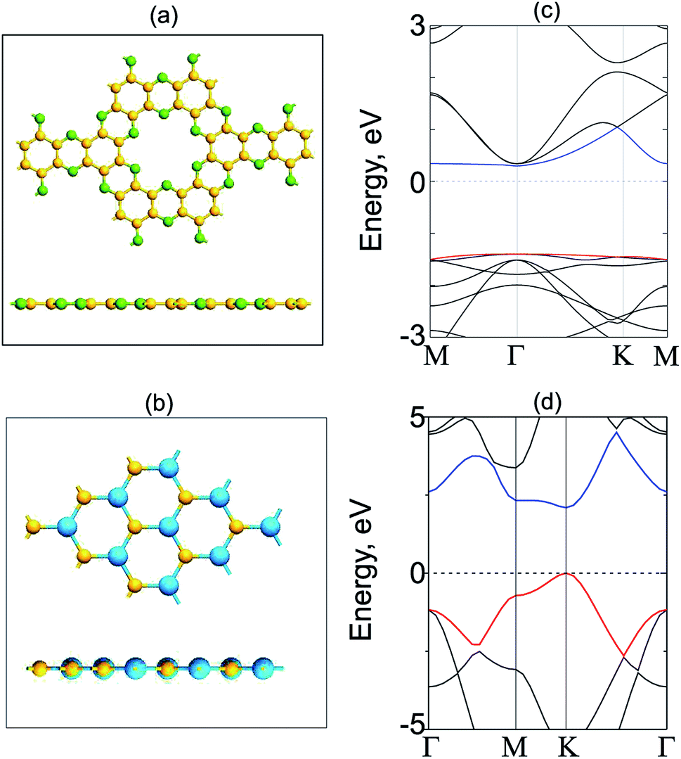 | ||
| Fig. 1 (a) and (b) are the atomic structures; (c) and (d) are the band structures of the C2N and GeC monolayers at the ground state. Yellow, green and blue balls stand for carbon, nitrogen and germanium atoms, respectively. Red and blue lines represent the valence band maximum (VBM) and conduction band minimum (CBM), respectively. | ||
We now construct GeC/C2N vdW-HTS by vertically placing GeC on top of C2N layer, as depicted in Fig. 2(a). In order to minimize the lattice mismatch in the lattice parameter between GeC and C2N monolayers, we use a model of a supercell, containing a (2 × 2) C2N unit cell and (5 × 5). It is clear that the C2N monolayer is known to be a flexible structure and it can withstand strains 12%.31 The lattice constants of GeC, C2N supercells are 16.32 Å, 16.66 Å, respectively. We set the average of the lattice constants of GeC and C2N supercells (16.44 Å) as the lattice constant of the corresponding GeC/C2N vdW-HTS. The overall lattice mismatch of GeC/C2N vdW-HST is only 1.18%. As a result, the electronic properties of GeC/C2N vdW-HTS are still unchanged under such small strain. It should be noted that this lattice mismatch is very small and is consistent with that in previous reports.52–56 The atomic structure of GeC/C2N vdW-HTS after the structural optimization is depicted in Fig. 2(a). The interlayer distance, defining by Deq between the GeC and C2N layers is obtained to be 3.43 Å. It is obvious that this Deq is similar to that of other typical vdW heterostructures, such as GaN/BlueP,57 TMDs/GaN,58 graphene/GaS,59 ZnO/GeC,60,61 C2N/MX (M = Ga, In; X = S, Se, Te)16,41,62 and so forth. Such result demonstrates the typical vdW forces are mainly contributed in GeC/C2N HTS. Moreover, our calculated binding energy in such HTS is −79.34 meV Å−2, which is also comparable with that in other typical vdW-HSTs. Furthermore, in order to check the structural distortion and stability of GeC/C2N vdW-HTS, we perform Ab initio molecular dynamics, as depicted in Fig. 2(b). One can observe that GeC/C2N retains its geometric structure without any structural distortion after 6 ps. Moreover, one can find from Fig. 2(b) that the total energy fluctuation is small, indicating that GeC/C2N vdW-HTS is thermally stable.
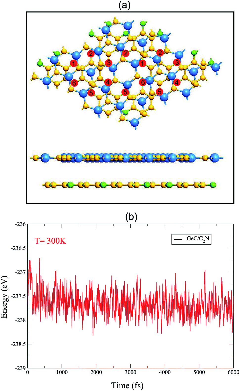 | ||
| Fig. 2 (a) Top view and side view of the relaxed atomic structure of GeC/C2N vdW-HTS. (b) Ab initio molecular dynamics calculation of the thermal stability of GeC/C2N vdW-HTS. | ||
Fig. 3 presents the electronic band structure of GeC/C2N vdW-HTS at the equilibrium state, along with that of the individual GeC and C2N monolayers. We can see that both the isolated GeC and C2N monolayers demonstrate the direct band gap semiconductors. When the GeC/C2N vdW-HTS is formed, it is obvious that its electronic band structure seems to be a combination between that of the individual GeC and C2N monolayers. This indicates the preservation of the intrinsic electronic properties of monolayers GeC and C2N in their GeC/C2N vdW-HTS. Moreover, we can observe that the band gap, forming in GeC/C2N vdW-HTS is significantly smaller than that of both GeC and C2N monolayers. The GeC/C2N vdW-HTS exhibits an indirect band gap semiconductor, which prevents the recombination of photoexcited electrons and holes, leading to a long carrier lifetime. As compared to the electronic band structures of GeC and C2N monolayers in Fig. 3(a) and (b), it can be seen that the VBM of such vdW-HTS is mainly contributed by the GeC layer, whereas the CBM of vdW-HTS comes from the CBM of C2N part, as displayed in Fig. 3(c). It also confirms the type-II band alignment, that is formed in such vdW-HTS. Interestingly, the type-II band alignment can be considered to improve the effective separation of electrons and holes. It demonstrates the advantage of such GeC/C2N vdW-HTS for designing optoelectronic devices that inhibit carrier recombination.
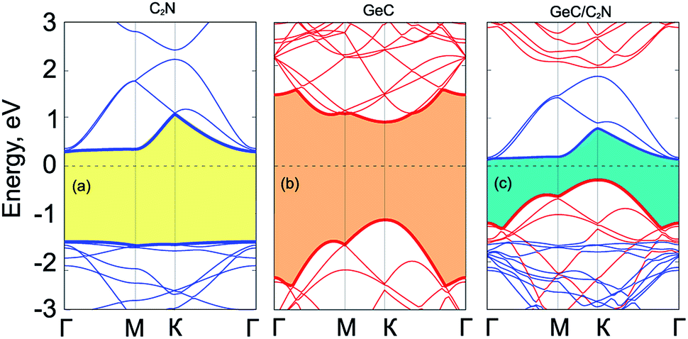 | ||
| Fig. 3 Electronic band structures of (a) monolayer C2N, (b) GeC and (c) GeC/C2N heterostructure. Red and blue lines represent the valence band maximum (VBM) and conduction band minimum (CBM), respectively. | ||
To have a clear picture of the charge transfer in GeC/C2N HST, we calculate its charge density difference, as shown in Fig. 4(a). We find that the charge densities distribution is mainly localized between the GeC and C2N layers. Moreover, one can observe that the electron is accumulated on the C2N layer and depleted on the GeC layer. The electron is likely transferred from the GeC to the C2N layers. The calculated work functions of isolated GeC and C2N monolayers are 4.91 eV and 5.68 eV, respectively, which confirm that the electrons are transported from the GeC to the C2N part in GeC/C2N vdW-HTS. This transportation results in a built-in electric field at the interface, leading to a reduction of the recombination of photogenerated electrons and holes. Fig. 4(b) shows the electrostatic potential of GeC/C2N HTS at the equilibrium state. We can see that the C2N layer has a deeper potential than the GeC layer. The difference in potential between the C2N and GeC layers is large of 13.4 eV at the equilibrium configuration, causing a charge transfer from the GeC to the C2N layers at the interface. Moreover, to confirm the existence of the vdW interactions between GeC and C2N monolayers, we further calculate the electron localization functions (ELFs) of GeC/C2N vdW-HTS, as depicted in Fig. 4(c). One can observe that there is no covalent bonding at the interfacial region of GeC/C2N vdW-HTS. From all of these findings, we can conclude that GeC/C2N vdW-HTS is featured via the weak vdW interactions.
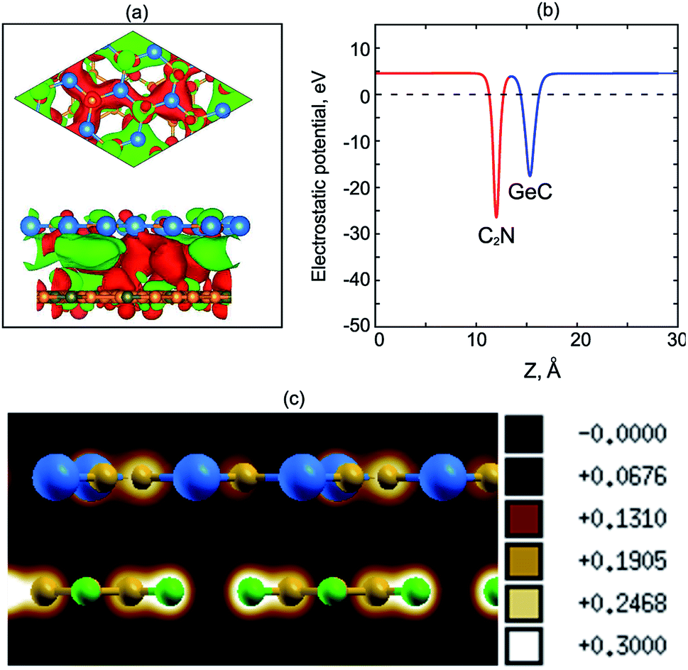 | ||
| Fig. 4 (a) Charge density difference and (b) electrostatic potential of GeC/C2N vdW-HTS. Red and green colors represent for the electron accumulation and depletion, respectively. (c) Electron localization functions of GeC/C2N vdW-HTS at the equilibrium state. | ||
The optical absorption coefficient of GeC/C2N vdW-HTS is depicted in Fig. 5. In addition, the absorption coefficient of individual constituent GeC and C2N monolayers are also calculated for comparison. We find that the capacity of light adsorption of the GeC/C2N vdW-HTS is enhanced as compared to that of individual constituent monolayers. Thus, the GeC/C2N vdW-HTS exhibits excellent light-absorption ability. More interestingly, we find that GeC/C2N vdW-HTS exhibits strong absorption in both visible and near ultra-violet regions with an intensity of 105 cm−1. It demonstrates that GeC/C2N vdW-HTS is an efficient material for photocatalysts and solar energy conversion.
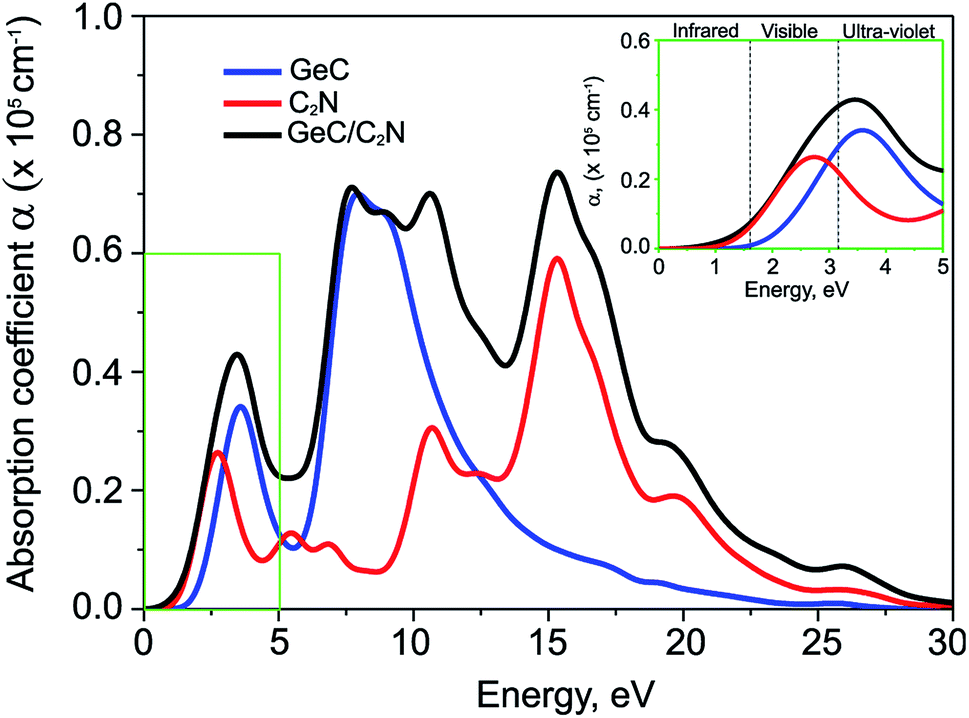 | ||
| Fig. 5 Calculated optical absorption coefficient of isolated GeC, C2N monolayers and their GeC/C2N vdW-HTS as a function of photon energy. | ||
Next, we will discuss the effects of electric field and strain engineering on the electronic properties of GeC/C2N vdW-HTS. The electric field applied perpendicularly along the z direction of the heterostructure, as illustrated in Fig. 6(a). The variation of the binding energy and band gap of GeC/C2N HTS under different strengths of electric fields is depicted in Fig. 6(b). We can see that applying an electric field tends to reduce the binding energy of the vdW-HTS. We find that the band gap of GeC/C2N vdW-HTS is very sensitive to the applied electric fields. The band gap depends not only on the strengths of the applied electric field, but also on its direction. When the positive electric field is applied, the band gap decreases with the increase of the positive electric field. Whereas, when the negative electric field is applied, the band gap increases with increasing the negative electric field. Interestingly, we find that GeC/C2N vdW-HTS changes from the semiconducting character to the metallic one when the positive electric field of +0.3 V Å−1 is applied. The semiconductor-to-metal transitions of GeC/C2N vdW-HTS make it a promising candidate for multifunctional nanodevices.
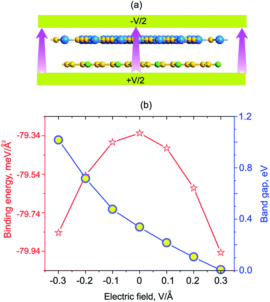 | ||
| Fig. 6 (a) Schematic model of the electric field, applying perpendicularly to the surface of GeC/C2N HTS. (b) Variation of the binding energy and band gap of GeC/C2N HTS as a function of the electric field. | ||
To get further insights into the physical mechanism of the band gap of GeC/C2N HTS under electric fields, we further calculate its band structures under different strengths of the applied electric fields, as depicted in Fig. 7. We can see that applying a positive electric field tends to shift downwards the CBM, while the VBM is shifted upwards. This trend leads to a decrease in the band gap of such HTS. Under the critical strength of the positive electric field of +0.3 V Å−1, the VBM of HTS moves upwards and crosses the Fermi level, resulting in a transition from semiconductor to metal. The nature of such a decrease in the band gap of vdW-HTS is due to the reduction of the built-in electric field when the positive electric field is applied, which is opposite to that of the built-in electric field. On the other hand, the band gap of HTS is increased from 0.42 eV to 1.10 eV with decreasing the strengths of the negative electric field from 0 V Å−1 to −0.3 V Å−1, respectively. The type-II band alignment in GeC/C2N HTS, in this case, is still maintained with the CBM from the C2N layer and the VBM from GeC one.
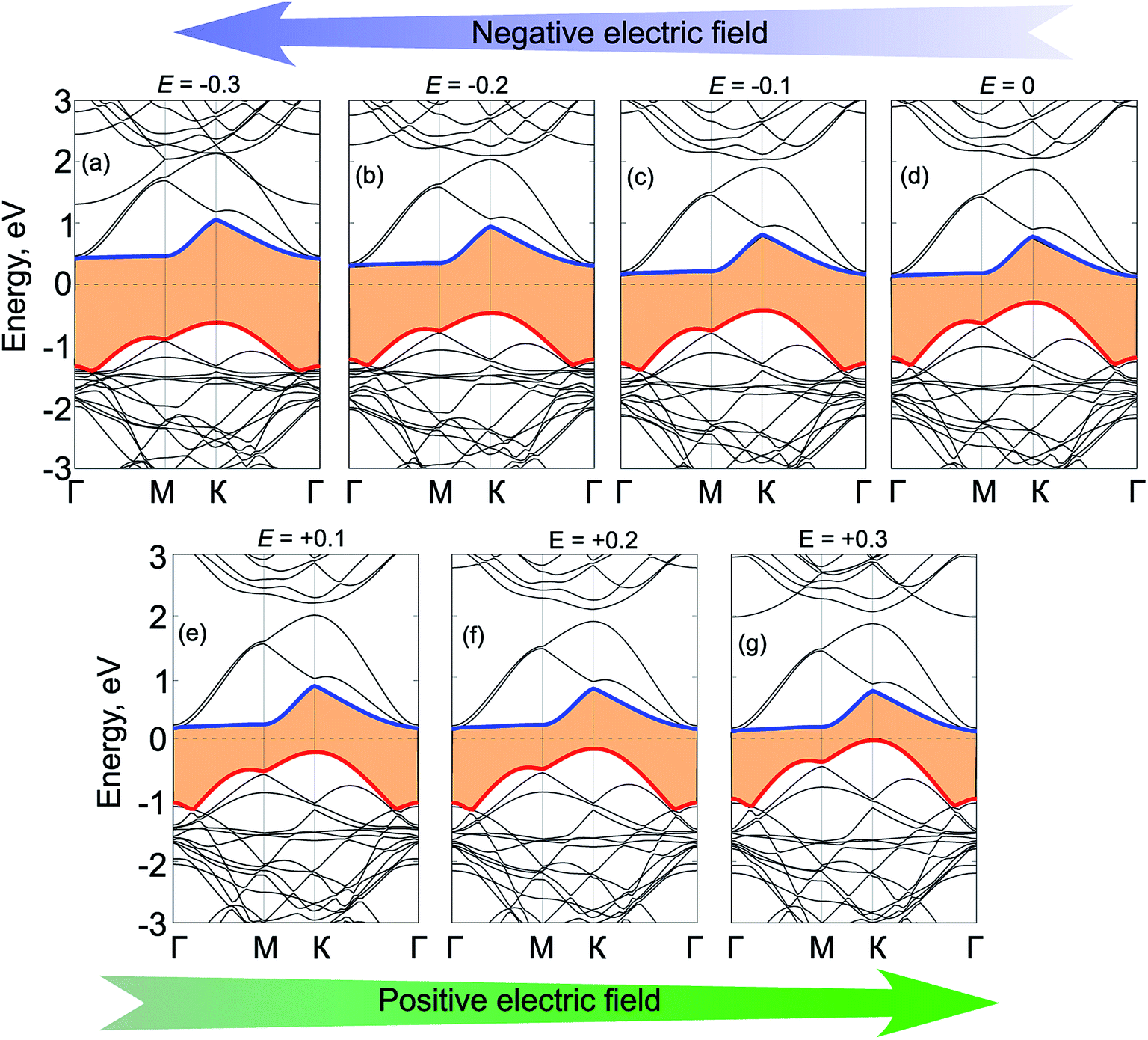 | ||
| Fig. 7 Band structures of GeC/C2N vdW-HTS under different strengths of electric fields, ranging from (a) −0.3 V Å−1, (b) −0.2 V Å−1, (c) −0.1 V Å−1, (d) 0 V Å−1, (e) +0.1 V Å−1, (f) +0.2 V Å−1, (g) +0.3 V Å−1. | ||
We now move to consider the case when the vertical strain is applied by changing the interlayer distance d between the GeC and C2N layers as follows: Δd = d0 − d, where d0 and d is the strained and equilibrium (unstrained) interlayer distance. The schematic model of the vertical strain is depicted in Fig. 7(a). The change in the binding energy and band gap of GeC/C2N HTS is also calculated and plotted in Fig. 7(b). It is obvious that GeC/C2N HTS has the smallest binding energy at the equilibrium interlayer distance of 3.43 Å. The band gap of GeC/C2N HTS under vertical strains changes via two different ways, as illustrated in Fig. 8(b). When the tensile strain is applied, i.e. Δd > 0, the band gap of vdW-HTS decreases from 0.42 eV to approximately 0 eV with increasing Δd from 0 Å to +0.9 Å, respectively. On the contrary, the band gap decreases from 0.42 eV to 0 eV with the decrease of the compressive strain from Δd = 0 Å to Δd = −0.9 Å, respectively. The physical mechanism of pressure-induced band gap narrowing is related to the positions of the VBM and CBM of GeC/C2N vdW-HTS under compressive strain. One can observe that the compressive strain has little effect on the vdW-HTS. Moreover, the band gaps narrowing when the interlayer distance is decreased can be explained by the fact that the compressive strain cannot facilitate electron transfer from the GeC to the C2N layer and the hole transfer from C2N to the GeC layer. Thus, the VBM upshifts towards the Fermi level, thus the band gap of the GeC/C2N vdW-HTS narrows. Also, it is obvious that the band gap of GeC/C2N vdW-HTS is more sensitive to the compressive strain than the tensile strain. However, as we can see from Fig. 8(b), both the compressive and tensile strains can cause the transition from semiconductor to the metal in GeC/C2N vdW-HTS.
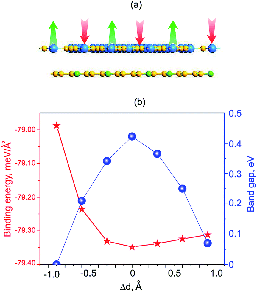 | ||
| Fig. 8 (a) Schematic model of GeC/C2N vdW-HTS under vertical strains. (b) Variation of the binding energy and band gap of GeC/C2N HTS as a function of strain engineering. | ||
Fig. 9 shows the electronic band structures of GeC/C2N vdW-HTS under compressive and tensile vertical strains. When the compressive strain is applied, i.e. Δd < 0, we can observe that both the VBM and CBM of such vdW-HTS move towards the Fermi level, leading to a decrease in the band gap. When a large compressive strain of Δd = −0.9 Å, both the CBM and VBM of GeC/C2N HTS cross the Fermi level, forming the metallic feature of such vdW-HTS. Similar to the compressive strain, the tensile strain also tends to shift the VBM and CBM of GeC/C2N vdW-HTS towards the Fermi level. This trend leads to a decrease in the band gap of the vdW-HTS and may cause the transition from semiconductor to metal under a large strain. Therefore, we can conclude that the GeC/C2N vdW-HTS is known to have an indirect band gap semiconductor and to feature the type-II band alignment, facilitating the effective separation of photogenerated electrons and holes. This is advantageous for fabricating optoelectronic devices that inhibit carrier recombination. Moreover, the optical absorption of GeC/C2N vdW-HTS is enhanced in both visible and near UV light as compared with that of the individual constituent monolayers, making it a promising candidate for light-absorption applications and solar energy conversion.
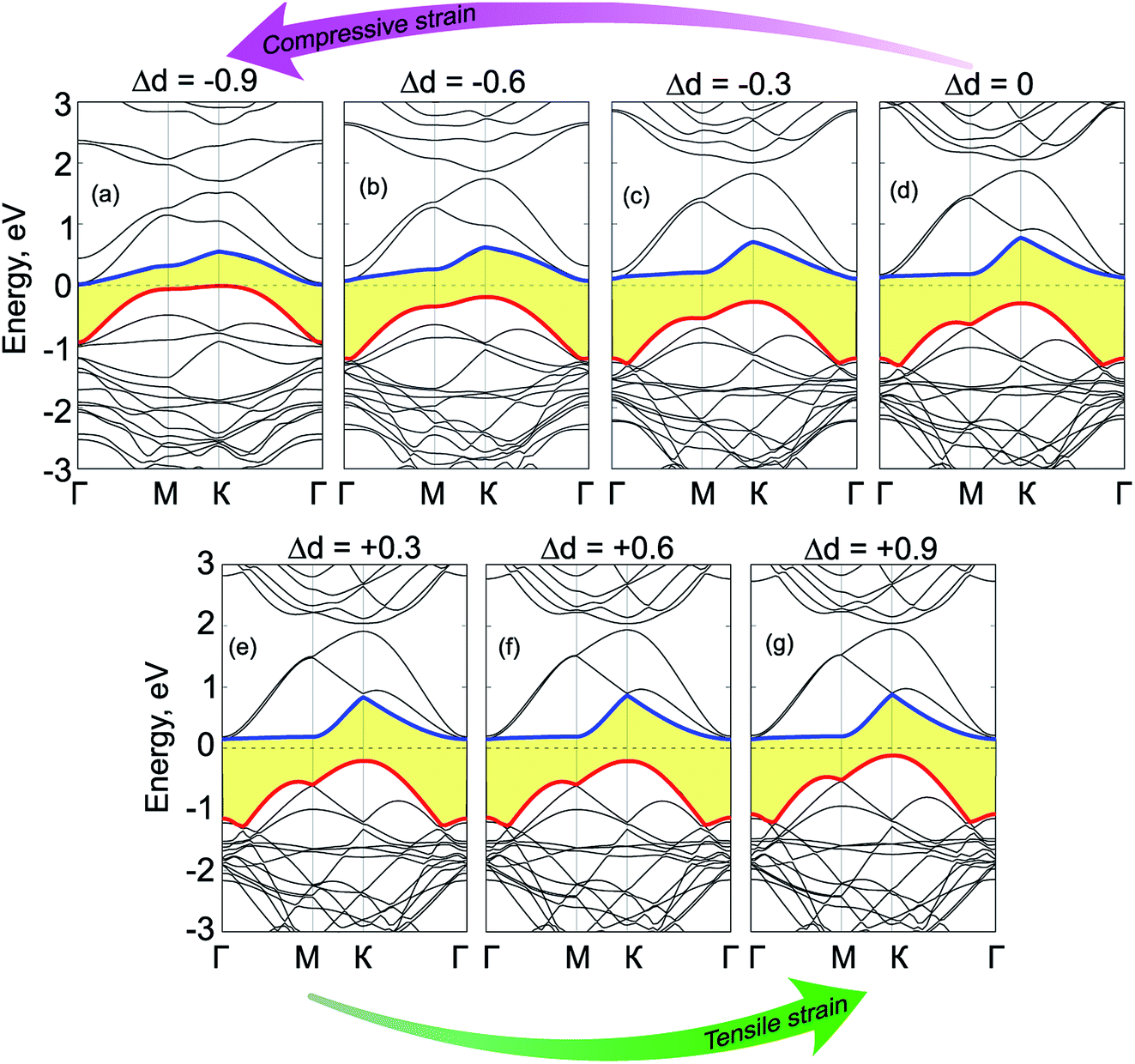 | ||
| Fig. 9 Band structures of GeC/C2N vdW-HTS under different strengths of electric fields, ranging from (a) Δd = −0.9 Å, (b) Δd = −0.6 Å, (c) Δd = −0.3 Å, (d) Δd = 0 Å, (e) Δd = + 0.3 Å, (f) Δd = + 0.6 Å, (g) Δd = + 0.9 Å. | ||
4. Conclusion
In summary, we have designed GeC/C2N vdW-HTS and systematically investigated its structure and electronic properties through first principles calculations. Our results show that GeC/C2N vdW-HTS is mainly characterized by the weak vdW interaction, leading to the preservation of the electronic features of both GeC and C2N monolayers. At the equilibrium state with the interlayer distance of 3.43 Å and the binding energy of −79.34 meV Å−2, we find that GeC/C2N HTS has a semiconductor with an indirect band gap of 0.42 eV, which is slightly smaller than that of the individual GeC and C2N monolayers. Moreover, GeC/C2N displays the type-II band alignment, confirming its ability for designing optoelectronic devices that inhibit carrier recombination. Besides, GeC/C2N vdW-HTS exhibits strong absorption in both visible and near-ultraviolet regions and its capacity of light adsorption is enhanced as compared to that of individual constituent monolayers. Furthermore, both the electric field and vertical strain can effectively tune the electronic properties of GeC/C2N vdW-HTS. The semiconductor to metal transition can emerge in GeC/C2N vdW-HTS when the positive electric field of +0.3 V Å−1 or the tensile vertical strain of −0.9 Å is applied. All these findings make GeC/C2N a promising candidate for future optoelectronic and nanoelectronic devices.Conflicts of interest
There are no conflicts to declare.Acknowledgements
This research is funded by Vietnam National Foundation for Science and Technology Development (NAFOSTED) under grant number 103.01-2019.05. B. Amin acknowledges support from the Higher Education Commission of Pakistan (HEC) under Project No. 5727/261 KPK/NRPU/R&D/HEC2016.References
- A. K. Geim and I. V. Grigorieva, Nature, 2013, 499, 419–425 CrossRef CAS PubMed.
- X. Wang and F. Xia, Nat. Mater., 2015, 14, 264 CrossRef CAS.
- X. Li, M.-W. Lin, J. Lin, B. Huang, A. A. Puretzky, C. Ma, K. Wang, W. Zhou, S. T. Pantelides and M. Chi, et al., Sci. Adv., 2016, 2, e1501882 CrossRef.
- C. R. Dean, A. F. Young, I. Meric, C. Lee, L. Wang, S. Sorgenfrei, K. Watanabe, T. Taniguchi, P. Kim and K. L. Shepard, et al., Nat. Nanotechnol., 2010, 5, 722 CrossRef CAS.
- Q. A. Vu, S. Fan, S. H. Lee, M.-K. Joo, W. J. Yu and Y. H. Lee, 2D Mater., 2018, 5, 031001 CrossRef.
- L. Yu, Y.-H. Lee, X. Ling, E. J. Santos, Y. C. Shin, Y. Lin, M. Dubey, E. Kaxiras, J. Kong and H. Wang, et al., Nano Lett., 2014, 14, 3055–3063 CrossRef CAS.
- H. Coy Diaz, J. Avila, C. Chen, R. Addou, M. C. Asensio and M. Batzill, Nano Lett., 2015, 15, 1135–1140 CrossRef CAS.
- G. Froehlicher, E. Lorchat and S. Berciaud, Phys. Rev. X, 2018, 8, 011007 CAS.
- X. Zhou, N. Zhou, C. Li, H. Song, Q. Zhang, X. Hu, L. Gan, H. Li, J. Lü and J. Luo, et al., 2D Mater., 2017, 4, 025048 CrossRef.
- T. Roy, M. Tosun, X. Cao, H. Fang, D.-H. Lien, P. Zhao, Y.-Z. Chen, Y.-L. Chueh, J. Guo and A. Javey, ACS Nano, 2015, 9, 2071–2079 CrossRef CAS PubMed.
- B. Peng, G. Yu, X. Liu, B. Liu, X. Liang, L. Bi, L. Deng, T. C. Sum and K. P. Loh, 2D Mater., 2016, 3, 025020 CrossRef.
- Y. Luo, K. Ren, S. Wang, J.-P. Chou, J. Yu, Z. Sun and M. Sun, J. Phys. Chem. C, 2019, 123, 22742–22751 CrossRef CAS.
- Y. Luo, S. Wang, K. Ren, J.-P. Chou, J. Yu, Z. Sun and M. Sun, Phys. Chem. Chem. Phys., 2019, 21, 1791–1796 RSC.
- K. Ren, M. Sun, Y. Luo, S. Wang, J. Yu and W. Tang, Appl. Surf. Sci., 2019, 476, 70–75 CrossRef CAS.
- T. Chen, L. Xu, Q. Li, X. Li and M. Long, Nanotechnology, 2019, 30, 445703 CrossRef CAS.
- K. D. Pham, N. N. Hieu, L. M. Bui, H. V. Phuc, B. D. Hoi, L. T. Tu, L. G. Bach, V. V. Ilyasov, B. Amin and M. Idrees, et al., Chem. Phys. Lett., 2019, 716, 155–161 CrossRef CAS.
- D. Chen, X. Lei, Y. Wang, S. Zhong, G. Liu, B. Xu and C. Ouyang, Appl. Surf. Sci., 2019, 497, 143809 CrossRef.
- X.-H. Li, B.-J. Wang, X.-L. Cai, L.-W. Zhang, G.-D. Wang and S.-H. Ke, RSC Adv., 2017, 7, 28393–28398 RSC.
- X.-H. Li, B.-J. Wang, X.-L. Cai, W.-Y. Yu, L.-W. Zhang, G.-D. Wang and S.-H. Ke, RSC Adv., 2017, 7, 44394–44400 RSC.
- J. Shang, S. Zhang, X. Cheng, Z. Wei and J. Li, RSC Adv., 2017, 7, 14625–14630 RSC.
- J. Mahmood, E. K. Lee, M. Jung, D. Shin, I.-Y. Jeon, S.-M. Jung, H.-J. Choi, J.-M. Seo, S.-Y. Bae and S.-D. Sohn, et al., Nat. Commun., 2015, 6, 6486 CrossRef CAS PubMed.
- B. Xu, H. Xiang, Q. Wei, J. Liu, Y. Xia, J. Yin and Z. Liu, Phys. Chem. Chem. Phys., 2015, 17, 15115–15118 RSC.
- H. Şahin, S. Cahangirov, M. Topsakal, E. Bekaroglu, E. Akturk, R. T. Senger and S. Ciraci, Phys. Rev. B: Condens. Matter Mater. Phys., 2009, 80, 155453 CrossRef.
- L. Pan, H. Liu, Y. Wen, X. Tan, H. Lv, J. Shi and X. Tang, Phys. Lett. A, 2011, 375, 614–619 CrossRef CAS.
- L. Hu and D. Wei, Phys. Chem. Chem. Phys., 2017, 19, 2235–2244 RSC.
- Y. Ji, H. Dong, T. Hou and Y. Li, J. Mater. Chem. A, 2018, 6, 2212–2218 RSC.
- K. Ren, M. Sun, Y. Luo, S. Wang, Y. Xu, J. Yu and W. Tang, Phys. Lett. A, 2019, 383, 1487–1492 CrossRef CAS.
- H. Yuan and R. S. Williams, Chem. Mater., 1993, 5, 479–485 CrossRef CAS.
- Z. Liu, J. Zhu, N. Xu and X. Zheng, Jpn. J. Appl. Phys., 1997, 36, 3625 CrossRef CAS.
- X. Wu, W. Zhang, L. Yan and R. Luo, Thin Solid Films, 2008, 516, 3189–3195 CrossRef CAS.
- S. Guan, Y. Cheng, C. Liu, J. Han, Y. Lu, S. A. Yang and Y. Yao, Appl. Phys. Lett., 2015, 107, 231904 CrossRef.
- T.-Y. Lü, X.-X. Liao, H.-Q. Wang and J.-C. Zheng, J. Mater. Chem., 2012, 22, 10062–10068 RSC.
- Z. Xu, Y. Li, Z. Liu and C. Li, Phys. E, 2016, 79, 198–205 CrossRef CAS.
- R. Zhang, B. Li and J. Yang, Nanoscale, 2015, 7, 14062–14070 RSC.
- Z. Zheng, X. Wang and W. Mi, Carbon, 2016, 109, 764–770 CrossRef CAS.
- D. Ma, Q. Wang, X. Yan, X. Zhang, C. He, D. Zhou, Y. Tang, Z. Lu and Z. Yang, Carbon, 2016, 105, 463–473 CrossRef CAS.
- Y. Ma, Y. Dai, M. Guo, C. Niu, L. Yu and B. Huang, Appl. Surf. Sci., 2011, 257, 7845–7850 CrossRef CAS.
- X. Gao, Y. Shen, Y. Ma, S. Wu and Z. Zhou, Appl. Phys. Lett., 2019, 114, 093902 CrossRef.
- K. Ren, C. Ren, Y. Luo, Y. Xu, J. Yu, W. Tang and M. Sun, Phys. Chem. Chem. Phys., 2019, 21, 9949–9956 RSC.
- X. Gao, Y. Shen, Y. Ma, S. Wu and Z. Zhou, Carbon, 2019, 146, 337–347 CrossRef CAS.
- Y. Bai, Q. Zhang, N. Xu, K. Deng and E. Kan, J. Phys. Chem. C, 2018, 122, 15892–15902 CrossRef CAS.
- D. Wang, D. Han, L. Liu and L. Niu, RSC Adv., 2016, 6, 28484–28488 RSC.
- Z. Zheng, X. Wang and W. Mi, Carbon, 2017, 117, 393–398 CrossRef CAS.
- R. Kumar, D. Das and A. K. Singh, J. Catal., 2018, 359, 143–150 CrossRef CAS.
- X. Wang, R. Quhe, W. Cui, Y. Zhi, Y. Huang, Y. An, X. Dai, Y. Tang, W. Chen and Z. Wu, et al., Carbon, 2018, 129, 738–744 CrossRef CAS.
- P. Giannozzi, S. Baroni, N. Bonini, M. Calandra, R. Car, C. Cavazzoni, D. Ceresoli, G. L. Chiarotti, M. Cococcioni, I. Dabo, A. D. Corso, S. de Gironcoli, S. Fabris, G. Fratesi, R. Gebauer, U. Gerstmann, C. Gougoussis, A. Kokalj, M. Lazzeri, L. Martin-Samos, N. Marzari, F. Mauri, R. Mazzarello, S. Paolini, A. Pasquarello, L. Paulatto, C. Sbraccia, S. Scandolo, G. Sclauzero, A. P. Seitsonen, A. Smogunov, P. Umari and R. M. Wentzcovitch, J. Phys.: Condens. Matter, 2009, 21, 395502 CrossRef PubMed.
- P. Giannozzi, O. Andreussi, T. Brumme, O. Bunau, M. B. Nardelli, M. Calandra, R. Car, C. Cavazzoni, D. Ceresoli, M. Cococcioni, N. Colonna, I. Carnimeo, A. D. Corso, S. de Gironcoli, P. Delugas, R. A. DiStasio, A. Ferretti, A. Floris, G. Fratesi, G. Fugallo, R. Gebauer, U. Gerstmann, F. Giustino, T. Gorni, J. Jia, M. Kawamura, H.-Y. Ko, A. Kokalj, E. Küçükbenli, M. Lazzeri, M. Marsili, N. Marzari, F. Mauri, N. L. Nguyen, H.-V. Nguyen, A. O. de-la Roza, L. Paulatto, S. Poncé, D. Rocca, R. Sabatini, B. Santra, M. Schlipf, A. P. Seitsonen, A. Smogunov, I. Timrov, T. Thonhauser, P. Umari, N. Vast, X. Wu and S. Baroni, J. Phys.: Condens. Matter, 2017, 29, 465901 CrossRef CAS PubMed.
- J. P. Perdew, K. Burke and M. Ernzerhof, Phys. Rev. Lett., 1996, 77, 3865 CrossRef CAS PubMed.
- W. Reckien, F. Janetzko, M. F. Peintinger and T. Bredow, J. Comput. Chem., 2012, 33, 2023–2031 CrossRef CAS PubMed.
- H. Sahin, Phys. Rev. B: Condens. Matter Mater. Phys., 2015, 92, 085421 CrossRef.
- Z. Xu, Y. Li, C. Li and Z. Liu, Appl. Surf. Sci., 2016, 367, 19–25 CrossRef CAS.
- X. Gao, Y. Shen, Y. Ma, S. Wu and Z. Zhou, J. Mater. Chem. C, 2019, 7, 4791–4799 RSC.
- Z. Guan, C.-S. Lian, S. Hu, S. Ni, J. Li and W. Duan, J. Phys. Chem. C, 2017, 121, 3654–3660 CrossRef CAS.
- X. Gao, Y. Shen, Y. Ma, S. Wu and Z. Zhou, Phys. Chem. Chem. Phys., 2019, 21, 15372–15379 RSC.
- X. Gao, Y. Shen, Y. Ma, S. Wu and Z. Zhou, Appl. Surf. Sci., 2019, 479, 1098–1104 CrossRef CAS.
- X. Gao, Y. Shen, Y. Ma, S. Wu and Z. Zhou, Phys. Status Solidi B, 2019, 1800759 CrossRef.
- K. Ren, S. Wang, Y. Luo, Y. Xu, M. Sun, J. Yu and W. Tang, RSC Adv., 2019, 9, 4816–4823 RSC.
- Z. Cui, K. Ren, Y. Zhao, X. Wang, H. Shu, J. Yu, W. Tang and M. Sun, Appl. Surf. Sci., 2019, 492, 513–519 CrossRef CAS.
- K. D. Pham, N. N. Hieu, H. V. Phuc, I. Fedorov, C. Duque, B. Amin and C. V. Nguyen, Appl. Phys. Lett., 2018, 113, 171605 CrossRef.
- G. Wang, L. Zhang, Y. Li, W. Zhao, A. Kuang, Y. Li, L. Xia, Y. Li and S. Xiao, J. Phys. D: Appl. Phys., 2019, 53, 015104 CrossRef.
- K. Ren, J. Yu and W. Tang, Phys. Lett. A, 2019, 383, 125916 CrossRef CAS.
- X. Wang, Y. Wang, R. Quhe, Y. Tang, X. Dai and W. Tang, J. Alloys Compd., 2019, 152559 Search PubMed.
| This journal is © The Royal Society of Chemistry 2020 |