
 Open Access Article
 This Open Access Article is licensed under a Creative Commons Attribution-Non Commercial 3.0 Unported Licence
Sub-millimeter size high mobility single crystal MoSe2 monolayers synthesized by NaCl-assisted chemical vapor deposition
Juncheng Li†
a,
Wenjie Yan†a,
Yanhui Lva,
Jian Lenga,
Duan Zhangb,
Cormac Ó Coileáinc,
Conor P. Cullenc,
Tanja Stimpel-Lindnerd,
Georg S. Duesbergcd,
Jiung Choe,
Miri Choif,
Byong Sun Chung,
Yanfeng Zhaoa,
Chengzhai Lva,
Sunil K. Arora h and
Han-Chun Wu*a
h and
Han-Chun Wu*a
aSchool of Physics, Beijing Institute of Technology, Beijing 100081, P. R. China. E-mail: wuhc@bit.edu.cn
bElementary Educational College, Beijing Key Laboratory for Nano-Photonics and Nano-Structure, Capital Normal University, Beijing 100048, P. R. China
cCentre for Research on Adaptive Nanostructures and Nanodevices (CRANN), Advanced Materials and Bioengineering Research (AMBER), School Chemistry, Trinity College Dublin, Ireland
dInstitute of Physics, EIT 2, Faculty of Electrical Engineering and Information Technology, Universität der Bundeswehr München, Germany
eWestern Seoul Center, Korea Basic Science Institute, Seoul 03579, Republic of Korea
fChuncheon Center, Korea Basic Science Institute, Chuncheon 24341, Republic of Korea
gDivision of Industrial Metrology, Korea Research Institute of Standards and Science, Daejeon 305-340, Republic of Korea
hCentre for Nanoscience and Nanotechnology, Panjab University, Chandigarh-160014, India
First published on 8th January 2020
Abstract
Monolayer MoSe2 is a transition metal dichalcogenide with a narrow bandgap, high optical absorbance and large spin-splitting energy, giving it great promise for applications in the field of optoelectronics. Producing monolayer MoSe2 films in a reliable and scalable manner is still a challenging task as conventional chemical vapor deposition (CVD) or exfoliation based techniques are limited due to the small domains/nanosheet sizes obtained. Here, based on NaCl assisted CVD, we demonstrate the simple and stable synthesis of sub-millimeter size single-crystal MoSe2 monolayers with mobilities ranging from 38 to 8 cm2 V−1 s−1. The average mobility is 12 cm2 V−1 s−1. We further determine that the optical responsivity of monolayer MoSe2 is 42 mA W−1, with an external quantum efficiency of 8.22%.
Introduction
Recently, transition metal dichalcogenides (TMDCs) have received considerable attention owing to their narrow direct bandgaps and great potential for use in electronics and optoelectronics, catalysts, capacitors, and novel heterostructures.1–3 MoSe2 is a TMDC with many unique properties and is a route to explore their applications.4–6 Phototransistors based on MoSe2 have been shown to display a very quick response time (<25 ms) at room temperature under ambient conditions.7,8 The edge sites of MoSe2 nanofilms and nanosheets have been found to be electrochemically active for H2.9,10 It has also been shown that mesoporous MoSe2 based anodes are an alternative for lithium ion batteries, with a reversible and stable storage capacity of 630 mA h g−1.11,12 Heterostructures incorporating MoSe2 have been reported to exhibit a strong photocurrent response and photovoltaic effect with high quantum efficiency.13 MoSe2 monolayers are the most promising candidate, among these materials, for applications in the field of optoelectronics due to the narrow direct bandgap (1.55 eV), high optical absorbance and large spin-splitting energy.2,4,11,14There are many different ways to produce MoSe2.4,14–16 However, producing monolayer MoSe2 films in a reliable and scalable manner is still a challenging task. The most common approaches are mechanical exfoliation and CVD.17–20 Although simple and convenient, exfoliation as a method usually suffers from some drawbacks. The product is usually multilayered, meaning it has an indirect bandgap and relatively weak optoelectronic performance.21 The lateral dimensions of exfoliated monolayer TMDCs are as small as a few tens of nm to several micrometers, which poses difficulties for its laboratory investigation and use.2 Furthermore, contamination in the exfoliation processes is unavoidable. Comparatively, CVD can produce larger, purer and monolayer materials.20,22 Reports on the CVD growth of MoSe2 suggest that it is extremely difficult to synthesize large area continuous monolayer films with solid-phase precursors because of the low chemical reactivity of Se.23–25 The CVD synthesis of MoSe2 results in triangular-shaped discontinuous domains of either single-layer MoSe2 or mixtures of single- and few-layer MoSe2.20,26,27 In addition, CVD is known to suffer from a lack of steady and durable output, which prevents its more widespread use for the production of monolayer MoSe2 films.28 To overcome some of the challenges associated with the CVD growth of TMDs using solid-phase precursors, recently NaCl has been used to assist the CVD growth of MoS2 and WS2 monolayers.29–31 It was found that the addition of NaCl led to an enhancement of the growth rate, reduced growth temperature and more continuous film production, due to formation of intermediate Na-containing species that reduce the energy of the reaction. The size of MoS2 and WS2 monolayers grown by this method were found to reach 300 μm (ref. 29) and 500 μm (ref. 31) respectively. However, to the best of our knowledge, there is little data on electrical and photoelectrical properties of TMDCs monolayers prepared by the NaCl assisted CVD method. In this work, we extended the above methodology to MoSe2 monolayer synthesis. Using NaCl assisted CVD, we have developed a simple and stable CVD method to synthesize large-scale, single crystal and monolayered MoSe2, whose size can be up to 250 μm. We also study the electrical and optoelectronic properties of the MoS2 monolayers in a four fingered back-gated field-effect transistor (FET) and find that they are n-type with an average mobility of 12 cm2 V−1 s−1 and responsivity of 42 mA W−1.
Results and discussion
Fig. 1(a) shows a schematic of the CVD growth system. MoO3 powder and Se particles were used as precursors. NaCl was used to assist the reaction. A SiO2 (300 nm)/Si substrate was put on the boat containing MoO3 powder with its polished surface facing downward in the quartz boat to receive sufficient mass flux of metal precursor. In conventional CVD, the process of MoSe2 monolayer growth is a step-by-step nucleation.29 The two main reactions involved in MoSe2 growth are:
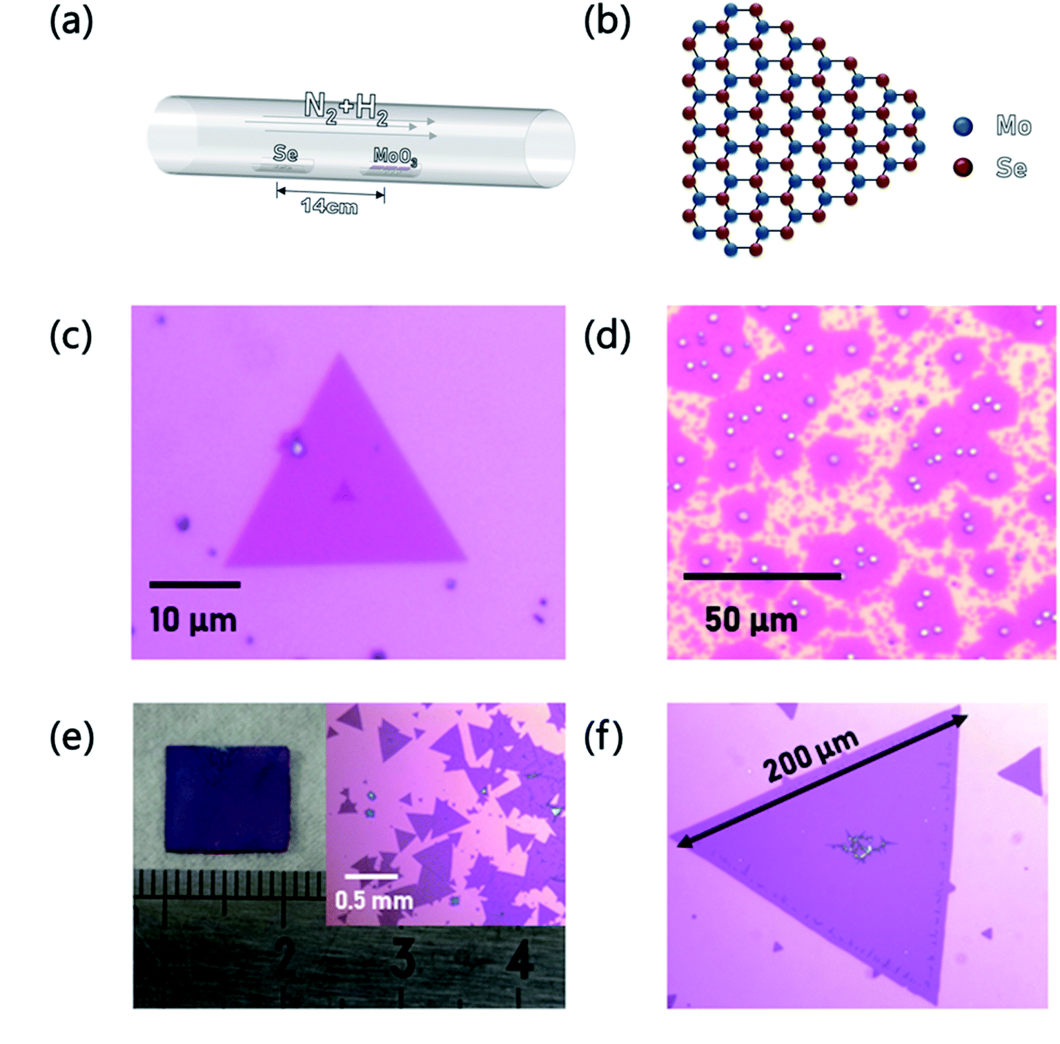 | ||
| Fig. 1 (a) Schematic of CVD growth system. (b) Atomistic model of monolayer MoSe2. (c) Image of MoSe2 grown by standard conditions without NaCl, using 15.6 mg MoO3 as the precursor. (d) Image of MoSe2 grown with the same conditions without NaCl, using 16.6 mg MoO3 as the precursor. (e) Typical appearance of prepared MoSe2 on the substrate. The dark purple layers, contrast with the pink substrate, are visible monolayers of MoSe2. (f) MoSe2 triangle of typical size of grown with the assistance of NaCl. | ||
The first reaction occurs mainly during the temperature ramp-up period while the second reaction, which is called an epitaxial process, takes place in the steady temperature period. As a result, the core-like dots at the center of many of the MoSe2 monolayers are essentially suboxide compounds, MoO3−xSey rather than the MoSe2 at the core. Moreover, the anisotropic growth of MoSe2 proceeds by different modes when there is a different ratio between Mo and Se, resulting in two kinds of edges, Mo-edges and Se-edges (Fig. 1(b)).31 When the ratio between Mo and Se atoms is close to 1![[thin space (1/6-em)]](https://www.rsc.org/images/entities/char_2009.gif) :2, the shape of the MoSe2 flakes looks like a regular hexagon. If Mo atoms are greater in abundance, the Mo-edge grows relatively faster.15,27,32 Following standard practice, when we use a relatively small quantity of MoO3 powder, the process yields low density small monolayer MoSe2 triangles. When more MoO3 is used, there is densely distributed isotropic MoSe2 (Fig. 1(c and d)). Clearly, the change of ratio between Mo and Se in the reaction, created by the great abundance of MoO3, results in the change in observed morphology.
:2, the shape of the MoSe2 flakes looks like a regular hexagon. If Mo atoms are greater in abundance, the Mo-edge grows relatively faster.15,27,32 Following standard practice, when we use a relatively small quantity of MoO3 powder, the process yields low density small monolayer MoSe2 triangles. When more MoO3 is used, there is densely distributed isotropic MoSe2 (Fig. 1(c and d)). Clearly, the change of ratio between Mo and Se in the reaction, created by the great abundance of MoO3, results in the change in observed morphology.
To overcome above issues, NaCl has been used to assist the CVD growth. In the NaCl assisted CVD method, NaCl has a two-fold effect on the growth process as below:33
| 2MoO3 + 2NaCl → MoO2Cl2↑ + Na2MoO4 |
| 3MoO3 + 2NaCl → MoO2Cl2↑ + Na2Mo2O7 |
First, it can accelerate the growth of MoSe2, with the formation of MoO2Cl2, which provides an opportunity for gas–gas phase reactions among MoO2Cl2, Se and H2. Secondly, it can increase the mass flux of the metal precursors by decreasing the melting point of MoO3, producing higher nucleation density. To avoid over-nucleation, a small quantity of MoO3 powder is used. Fig. 1(e) shows a typical optical image of a monolayer MoSe2 film grown by NaCl assisted CVD. It shows both large-scale and dense monolayer MoSe2 coverage. The typical lateral size of MoSe2 grown with the NaCl assisted CVD is more than 200 μm (Fig. 1(f)), and some can reach up to 500 μm.
Fig. 2(a) shows an atomic force microscopy (AFM) image of as-prepared MoSe2. Clear contrast between the SiO2/Si substrate and MoSe2 indicates that the thickness is ∼0.82 nm. In addition to verifying the uniformity of the layers, we also identify the phase of the complete monolayer as MoSe2 using the Raman spectroscopy (Fig. 2(b)).28 The Raman spectra consists of two main peaks at 240 cm−1 and 520 cm−1. The peak at 520 cm−1 is the characteristic Raman peak of the Si, while the one at 240 cm−1 indicates the dominance of the A1g mode, the out of plane vibration, of MoSe2.34,35 We also find Raman peaks at 169 cm−1, 289 cm−1 and 361 cm−1, corresponding the E1g, E2g and A2g, modes of MoSe2 respectively. We used transmission electron microscopy (TEM) to verify the monolayer nature and crystal structure of the MoSe2. The measured width of the lattice fringes is 0.27 nm which is in agreement with reports on the distance between the adjacent atoms.5 Selected-area-electron-diffraction (SAED) images of MoSe2 (inset of Fig. 2(c)) exhibit one set of six-fold symmetry diffraction spots, confirming its highly crystalline monolayer nature. From energy-dispersive X-ray spectroscopy (EDS) mapping of a MoSe2 sample exposed to atmosphere, the ratio between Mo and Se atoms is determined to be close to 1:2, displaying the stability of MoSe2. The stability of MoSe2 and its adhesion to the Si/SiO2 substrate was further checked by soaking it in water, ethanol and acetone. Fig. 2(e) shows X-ray photoelectron spectroscopy (XPS) core level spectra of the Mo-3d and Se-3d core-levels of the as grown MoSe2 monolayer films measured at 300 K. From the data we can determine that there is only one major state for the Mo and two states for Se atoms, the binding energy for the Mo–Se Mo 3d5/2 state is 229.1 eV. While the corresponding values for the Se 3d5/2 55.5 eV. Both elements showed minor components at higher binding energies attributed to surface oxygen absorption as the sample was exposed to ambient conditions for an extended period.36
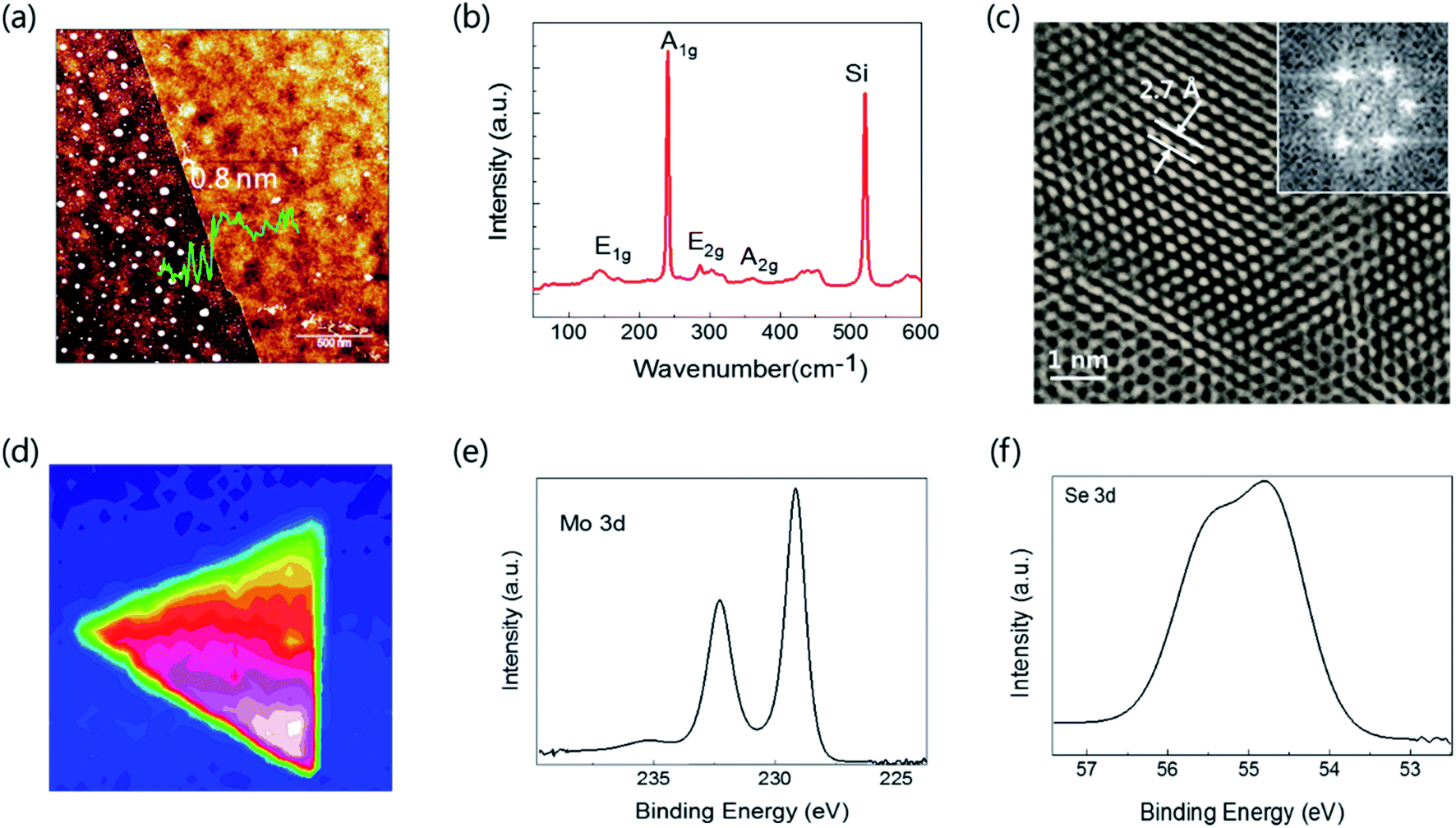 | ||
| Fig. 2 (a) AFM height map of MoSe2 sample on growth substrate. Also shown in the figure is the height profile near the edge of a MoSe2 domain. (b) Raman spectra of MoSe2 sample, showing the major observed peaks. (c) High resolution TEM image of MoSe2 sample with its selected area diffraction pattern shown in the inset. (d) Raman mapping of MoSe2 sample. (e and f) XPS spectra recorded for Mo 3d and Se 3d edges at room temperature for monolayer MoSe2 sample. | ||
In order to study the electrical and optoelectronic properties of MoSe2, we fabricated four-finger back-gated field-effect transistors. The output and transfer characteristics of a MoSe2 FET is shown in Fig. 3. The output and transfer characteristics are evidence of the n-type nature of the MoSe2, which is in-line with the previous studies.16,31,37,38 Fig. 3(a and b) shows the Id–Vd characteristic under gate voltages ranging from −16 V to +4 V. The curve shows the obvious semiconducting nature of MoSe2, whose resistance decreases as the bias voltage increases. In contrast with conventional FETs, there is no apparent saturation in the drain current the FETs fabricated from MoSe2. The switching voltage without a gate voltage is about 12 V, while the positive/negative gate voltage can decrease/increase the switching voltage. As expected, gate voltage can modulate the conductivity of the FET. Fig. 3(c) exhibits the Id–Vg characteristic measured under different bias voltage. The FET is depleted from free carriers when Vg is lower than 0 V. The switch ratio, Ion/Ioff, under +4 V of bias voltage, can reach 105.39–42 The transfer characteristic offers the opportunity to compute the mobility of the FET. Using the formula  , we find that the mobility μ is 20.1 cm2 V−1 s−1. In this formula, L and W are the length and width of the conduction channel, respectively, and CSiO2 = ε0εr/d is capacitance per unit area estimated for the gate dielectric, with ε0 being the free-space permittivity, εr, the relative permittivity for SiO2, being 3.9, and d, the thickness of the SiO2, being 300 nm. More than 20 devices were fabricated and characterized. It was found that the mobility ranged from 38 to 8 cm2 V−1 s−1 (Fig. 3(d)), with an average 12 cm2 V−1 s−1. The highest mobility found for our samples is very close to the reported value (50 cm2 V−1 s−1) for mechanically exfoliated ultra-thin MoSe2.43 The reduced mobility can be attributed to imperfections in the monolayers, such as Se vacancies, which might be improved by reducing nuclei density, controlling the mass flux or growth rate, etc.31
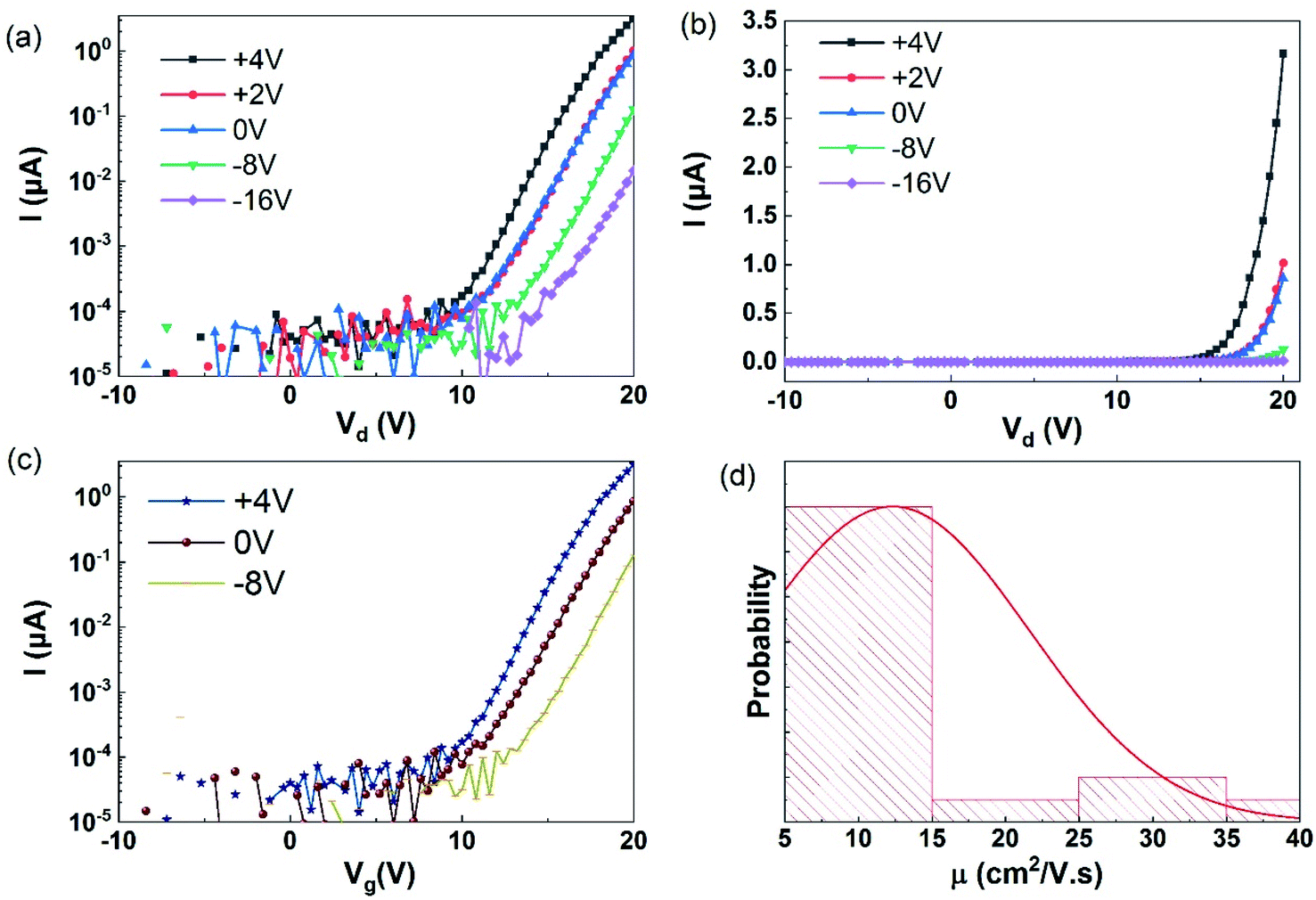 | ||
| Fig. 3 (a) The I–Vd curves of the MoSe2 FET under various gate voltages plotted on a log scale and (b) on a linear scale. (c) Transfer characteristic curve of the FET under various bias voltages. (d) Distribution of the mobility of all devices measured. | ||
In order to realize the potential of monolayer MoSe2 for applications in solar cells, photosensitive sensor and other devices,18,44 it is also necessary to investigate it optoelectronic properties. We measured the optoelectronic responsivity in ambient conditions with different voltages and light sources of different wavelengths. Fig. 4(a) exhibits the quick response time of the FET under the 200–500 mW cm−2 power laser with a 635 nm wavelength. The bias voltage is 10 V and the gate voltage is 10 V. Under such conditions, the photocurrent ranges between a few to hundreds of nanoamperes. When the laser power is increased sufficiently, there is saturation of the photo-enhancement of the drain current as can be seen in Fig. 4(b). We also investigate the time response of the gated FET under pulsed 400 mW cm−2 illumination (Fig. 4(c)). It is apparent that a positive gate voltage not only elevates the drain current in both dark and lit condition, but also increases the photo current, while a negative gate voltage has no such effect. We show the power dependence of the Iphoto in Fig. 4(d) derived from the Fig. 4(b), which intuitively presents the modulation of the bias voltage and the laser power. When the bias voltage climbs into a certain range, the photo current can be modulated by the power intensity, which is shown in Fig. 4(d). We determine the responsivity of the FET to be 42 mA W−1, and the external quantum efficiency (EQE) of the device is 8.22%. Table 1 summarizes the electrical and optoelectronic properties of MoSe2 from other studies from literature. Clearly, it is rather difficult to synthesize both high-mobility and large-scale monolayer MoSe2. Using NaCl assisted CVD method, it is relatively easy to synthesize large monolayer MoSe2 with sound electrical and optoelectronic properties.
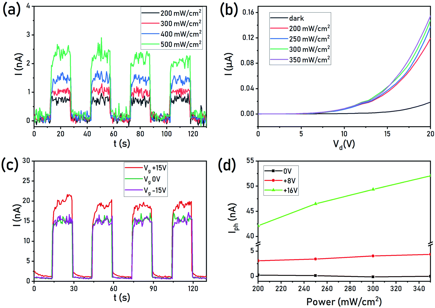 | ||
| Fig. 4 (a) I–t characteristic plots for FET for a variety of power intensities of a 635 nm laser. (b) The output characteristic of the FET under different power intensities of 635 nm laser. (c) I–t characteristic curve of the FET under different gate voltages for the 635 nm laser. (d) The Iphoto–power curve of the FET under different bias voltages. | ||
| Type | Method | Mobility (cm2 V−1 s−1) | Responsivity (mA W−1) | Size (μm) | Reference |
|---|---|---|---|---|---|
| Monolayer | CVD | 23 | — | ∼5 | 8 |
| Film | CVD | 0.02 | — | ∼0.2 (grain size) | 26 |
| Multilayer | CVD | 121 | — | Several hundred | 37 |
| Monolayer | CVD | 50 | — | 135 | 34 |
| Multilayer | Micromechanical exfoliation | 50 | — | 1–3 | 16 |
| Monolayer | CVD | — | 13 | >50 | 21 |
| Ultra-thin | Mechanical exfoliation | 50.5 | — | <44 μm | 43 |
| Multilayer | Mechanical exfoliation | 19.7 | 97100 |
∼30 | 45 |
| Multilayer | Atomic layer deposition | — | 11.7 | Several hundred | 46 |
| Multilayer | Mechanical exfoliation | 30–35 | — | ∼10 | 47 |
| Monolayer | CVD | 42 | — | Several hundred | 48 |
| Multilayer | CVD | 10 | 93700 |
3–4 | 49 |
| Multilayer | Mechanical exfoliation | 50.6 | 519200 |
∼10 | 50 |
| Few layer | Mechanical exfoliation | 5.1 | 238000 |
∼25 | 51 |
| Monolayer | CVD | 38 | 42 | Several hundred | Our work |
Conclusion
In conclusion, we have found an effective and convenient method to synthesize large-scale monolayer MoSe2 and investigated the optoelectronic properties of derived FETs. When as-prepared MoSe2 was used to fabricate FETs, it had a mobility up to 38 cm2 V−1 s−1 and a responsivity of 42 mA W−1, which is promising for its practical application.Materials and methods
Sample preparation and characterization
For the reaction, 0.5 g of selenium granules and 5–7 mg of a mixture of MoO3 powder and 1 mg of sodium chloride powder, were prepared as precursors. We used a quartz boat containing selenium granules and another boat with the mixed NaCl and MoO3 powder to obtain layered MoSe2 by the selenization of MoO3. Before heating the furnace, 100 standard cubic meter per minute (sccm) of the mixture of H2/N2 (10:90) carrier gas was used to purge the tube for 20 minutes. The furnace was heated to 750 °C in 15 minutes with the rate of 50 °C per minute, and a reaction dwell time of 15 minutes was used, after which the furnace was allowed to cool naturally. During the heating and reaction process, the flow rate of the carrier gas was kept at 50 sccm, giving a H2 flow of 5 sccm. The pressure inside the tube was maintained at 30 Torr. Atomic force microscopy (Bruker Multi-mode 8, in peak force tapping mode), Raman spectroscopy (Bruker Senterra confocal spectrometer with an excitation wavelength of 532 nm), Transmission electronic microscopy (JEOL JEM-2100F at 200 kV with a probe size under 0.5 nm), and XPS (micro-XPS, PHI Versa Probe III) were used to characterize the MoSe2 samples, identifying its single-layer and high-quality nature. In Raman spectroscopy measurements, the wavelength of the laser used was 532 nm.
Device fabrication and measurement
The MoSe2 films were transferred onto new 300 nm SiO2/Si substrates using a PMMA assisted transfer method. Ultraviolet lithography was then used to pattern the electrodes. We deposited Ti–Au electrodes with 15 nm of Ti and 55 nm of Au using electron beam evaporation. The channel lengths and widths were 4 μm and 50 μm respectively. For electrical measurements, the devices was placed in a darkness, except for when required, and at room-temperature. In all experiments the source was grounded.Author contributions
H. C. W. conceived the study. J. C. L., and J. L. grew the sample. W. J. Y., Y. H. L. and D. Z. performed the Raman measurements. C. C. conducted the AFM characterization. C. P. C., T. S., and G. S. D. performed the XPS characterization. J. C., M. C., and B. S. C. carried out the TEM measurements. Y. F. Z., C. Z. L. and S. K. A. helped with device fabrication and data analysis. H. C. W. and J. C. L. wrote the manuscript. All authors discussed the results and commented on the manuscript.Conflicts of interest
There is no conflicts to declare.Acknowledgements
This work was supported by the National Key Research and Development Program under grant No. 2017YFA0303800 and 2017YFE0301404, the National Natural Science Foundation of China (No. 61874010, 11804237), and by the Science and Technology Innovation Program for Creative Talents in Beijing Institute of Technology (No. 2017CX01006). G. S. D. acknowledges the support of SFI under Contract No. PI_15/IA/3131.References
- L. Kou, T. Frauenheim and C. Chen, Nanoscale Multilayer Transition-Metal Dichalcogenide Heterostructures: Band Gap Modulation by Interfacial Strain and Spontaneous Polarization, J. Phys. Chem. Lett., 2013, 4(10), 1730–1736, DOI:10.1021/jz400668d.
- M. Pumera, Z. Sofer and A. Ambrosi, Layered transition metal dichalcogenides for electrochemical energy generation and storage, J. Mater. Chem. A, 2014, 2(24), 8981–8987 RSC.
- M. Bernardi, M. Palummo and J. C. Grossman, Extraordinary sunlight absorption and one nanometer thick photovoltaics using two-dimensional monolayer materials, Nano Lett., 2013, 13(8), 3664–3670 CrossRef CAS PubMed.
- S. Tongay, J. Zhou, C. Ataca, K. Lo, T. S. Matthews, J. Li, J. C. Grossman and J. Wu, Thermally driven crossover from indirect toward direct bandgap in 2D semiconductors: MoSe2 versus MoS2, Nano Lett., 2012, 12(11), 5576–5580 CrossRef CAS PubMed.
- Y. Zhang, T. R. Chang, B. Zhou, Y. T. Cui, H. Yan, Z. Liu, F. Schmitt, J. Lee, R. Moore, Y. Chen, H. Lin, H. T. Jeng, S. K. Mo, Z. Hussain, A. Bansil and Z. X. Shen, Direct observation of the transition from indirect to direct bandgap in atomically thin epitaxial MoSe2, Nat. Nanotechnol., 2014, 9(2), 111–115 CrossRef CAS PubMed.
- K. F. Mak and J. Shan, Photonics and optoelectronics of 2D semiconductor transition metal dichalcogenides, Nat. Photonics, 2016, 10(4), 216–226 CrossRef CAS.
- A. Kumar and P. K. Ahluwalia, Electronic structure of transition metal dichalcogenides monolayers 1H-MX2 (M = Mo, W; X = S, Se, Te) from ab-initio theory: new direct band gap semiconductors, Eur. Phys. J. B, 2012, 85(6), 186 CrossRef.
- Y. H. Chang, W. Zhang, Y. Zhu, Y. Han, J. Pu, J. K. Chang, W. T. Hsu, J. K. Huang, C. L. Hsu, M. H. Chiu, T. Takenobu, H. Li, C. I. Wu, W. H. Chang, A. T. Wee and L. J. Li, Monolayer MoSe2 grown by chemical vapor deposition for fast photodetection, ACS Nano, 2014, 8(8), 8582–8590 CrossRef CAS PubMed.
- C. Xu, S. Peng, C. Tan, H. Ang, H. Tan, H. Zhang and Q. Yan, Ultrathin S-doped MoSe2 nanosheets for efficient hydrogen evolution, J. Mater. Chem. A, 2014, 2(16), 5597–5601 RSC.
- C. Tsai, K. Chan, F. Abild-Pedersen and J. K. Norskov, Active edge sites in MoSe2 and WSe2 catalysts for the hydrogen evolution reaction: a density functional study, Phys. Chem. Chem. Phys., 2014, 16(26), 13156–13164 RSC.
- Y. Shi, C. Hua, B. Li, X. Fang, C. Yao, Y. Zhang, Y.-S. Hu, Z. Wang, L. Chen, D. Zhao and G. D. Stucky, Highly Ordered Mesoporous Crystalline MoSe2 Material with Efficient Visible-Light-Driven Photocatalytic Activity and Enhanced Lithium Storage Performance, Adv. Funct. Mater., 2013, 23(14), 1832–1838 CrossRef CAS.
- B. Shin, Y. Zhu, N. A. Bojarczuk, S. J. Chey and S. Guha, Control of an interfacial MoSe2 layer in Cu2ZnSnSe4 thin film solar cells: 8.9% power conversion efficiency with a TiN diffusion barrier, Appl. Phys. Lett., 2012, 101(5), 053903 CrossRef.
- Y. Gong, S. Lei, G. Ye, B. Li, Y. He, K. Keyshar, X. Zhang, Q. Wang, J. Lou, Z. Liu, R. Vajtai, W. Zhou and P. M. Ajayan, Two-Step Growth of Two-Dimensional WSe2/MoSe2 Heterostructures, Nano Lett., 2015, 15(9), 6135–6141 CrossRef CAS PubMed.
- J. C. Shaw, H. Zhou, Y. Chen, N. O. Weiss, Y. Liu, Y. Huang and X. Duan, Chemical vapor deposition growth of monolayer MoSe2 nanosheets, Nano Res., 2014, 7(4), 511–517 CrossRef CAS.
- S. Larentis, B. Fallahazad and E. Tutuc, Field-effect transistors and intrinsic mobility in ultra-thin MoSe2 layers, Appl. Phys. Lett., 2012, 101(22), 223104 CrossRef.
- J. N. Coleman, M. Lotya, A. O'Neill, S. D. Bergin, P. J. King, U. Khan, K. Young, A. Gaucher, S. De, R. J. Smith, I. V. Shvets, S. K. Arora, G. Stanton, H. Y. Kim, K. Lee, G. T. Kim, G. S. Duesberg, T. Hallam, J. J. Boland, J. J. Wang, J. F. Donegan, J. C. Grunlan, G. Moriarty, A. Shmeliov, R. J. Nicholls, J. M. Perkins, E. M. Grieveson, K. Theuwissen, D. W. McComb, P. D. Nellist and V. Nicolosi, Two-dimensional nanosheets produced by liquid exfoliation of layered materials, Science, 2011, 331(6017), 568–571 CrossRef CAS PubMed.
- D. Jariwala, V. K. Sangwan, L. J. Lauhon, T. J. Marks and M. C. Hersam, Emerging device applications for semiconducting two-dimensional transition metal dichalcogenides, ACS Nano, 2014, 8(2), 1102–1120 CrossRef CAS PubMed.
- J. Shen, Y. He, J. Wu, C. Gao, K. Keyshar, X. Zhang, Y. Yang, M. Ye, R. Vajtai, J. Lou and P. M. Ajayan, Liquid Phase Exfoliation of Two-Dimensional Materials by Directly Probing and Matching Surface Tension Components, Nano Lett., 2015, 15(8), 5449–5454 CrossRef CAS PubMed.
- R. Ge, X. Wu, M. Kim, J. Shi, S. Sonde, L. Tao, Y. Zhang, J. C. Lee and D. Akinwande, Atomristor: Nonvolatile Resistance Switching in Atomic Sheets of Transition Metal Dichalcogenides, Nano Lett., 2018, 18(1), 434–441 CrossRef CAS PubMed.
- J. Xia, X. Huang, L. Z. Liu, M. Wang, L. Wang, B. Huang, D. D. Zhu, J. J. Li, C. Z. Gu and X. M. Meng, CVD synthesis of large-area, highly crystalline MoSe2 atomic layers on diverse substrates and application to photodetectors, Nanoscale, 2014, 6(15), 8949–8955 RSC.
- Q. H. Wang, K. Kalantar-Zadeh, A. Kis, J. N. Coleman and M. S. Strano, Electronics and optoelectronics of two-dimensional transition metal dichalcogenides, Nat. Nanotechnol., 2012, 7(11), 699–712 CrossRef CAS PubMed.
- Y. Shi, H. Li and L. J. Li, Recent advances in controlled synthesis of two-dimensional transition metal dichalcogenides via vapour deposition techniques, Chem. Soc. Rev., 2015, 44(9), 2744–2756 RSC.
- A. S. Pawbake, M. S. Pawar, S. R. Jadkar and D. J. Late, Large area chemical vapor deposition of monolayer transition metal dichalcogenides and their temperature dependent Raman spectroscopy studies, Nanoscale, 2016, 8(5), 3008–3018 RSC.
- M. I. B. Utama, X. Lu, Y. W. Yuan and Q. H. Xiong, Detrimental influence of catalyst seeding on the device properties of CVD-grown 2D layered materials: a case study on MoSe2, Appl. Phys. Lett., 2014, 105(25), 253102 CrossRef.
- D. Hu, G. Xu, L. Xing, X. Yan, J. Wang, J. Zheng, Z. Lu, P. Wang, X. Pan and L. Jiao, Two-Dimensional Semiconductors Grown by Chemical Vapor Transport, Angew. Chem., Int. Ed., 2017, 56(13), 3611–3615 CrossRef CAS PubMed.
- X. Lu, M. I. Utama, J. Lin, X. Gong, J. Zhang, Y. Zhao, S. T. Pantelides, J. Wang, Z. Dong, Z. Liu, W. Zhou and Q. Xiong, Large-area synthesis of monolayer and few-layer MoSe2 films on SiO2 substrates, Nano Lett., 2014, 14(5), 2419–2425 CrossRef CAS PubMed.
- X. Song, Z. Guo, Q. Zhang, P. Zhou, W. Bao and D. W. Zhang, Progress of Large-Scale Synthesis and Electronic Device Application of Two-Dimensional Transition Metal Dichalcogenides, Small, 2017, 13(35), 1700098 CrossRef PubMed.
- H. Li, Y. Li, A. Aljarb, Y. Shi and L. J. Li, Epitaxial Growth of Two-Dimensional Layered Transition-Metal Dichalcogenides: Growth Mechanism, Controllability, and Scalability, Chem. Rev., 2018, 118(13), 6134–6150 CrossRef CAS PubMed.
- Y. P. Shi, P. F. Yang, S. L. Jiang, Z. P. Zhang, Y. H. Huan, C. Y. Xie, M. Hong, J. P. Shi and Y. F. Zhang, Na-assisted fast growth of large single-crystal MoS2 on sapphire, Nanotechnology, 2019, 30(3), 034002 CrossRef CAS PubMed.
- Z. Wang, Y. Xie, H. Wang, R. Wu, T. Nan, Y. Zhan, J. Sun, T. Jiang, Y. Zhao, Y. Lei, M. Yang, W. Wang, Q. Zhu, X. Ma and Y. Hao, NaCl-assisted one-step growth of MoS2-WS2 in-plane heterostructures, Nanotechnology, 2017, 28(32), 325602 CrossRef PubMed.
- J. Zhou, J. Lin, X. Huang, Y. Zhou, Y. Chen, J. Xia, H. Wang, Y. Xie, H. Yu, J. Lei, D. Wu, F. Liu, Q. Fu, Q. Zeng, C. H. Hsu, C. Yang, L. Lu, T. Yu, Z. Shen, H. Lin, B. I. Yakobson, Q. Liu, K. Suenaga, G. Liu and Z. Liu, A library of atomically thin metal chalcogenides, Nature, 2018, 556(7701), 355–359 CrossRef CAS PubMed.
- J. Chen, B. Liu, Y. Liu, W. Tang, C. T. Nai, L. Li, J. Zheng, L. Gao, Y. Zheng, H. S. Shin, H. Y. Jeong and K. P. Loh, Chemical Vapor Deposition of Large-Sized Hexagonal WSe2 Crystals on Dielectric Substrates, Adv. Mater., 2015, 27(42), 6722–6727 CrossRef CAS PubMed.
- X. Duan, C. Wang, J. C. Shaw, R. Cheng, Y. Chen, H. Li, X. Wu, Y. Tang, Q. Zhang, A. Pan, J. Jiang, R. Yu, Y. Huang and X. Duan, Lateral epitaxial growth of two-dimensional layered semiconductor heterojunctions, Nat. Nanotechnol., 2014, 9(12), 1024–1030 CrossRef CAS PubMed.
- X. Wang, Y. Gong, G. Shi, W. L. Chow, K. Keyshar, G. Ye, R. Vajtai, J. Lou, Z. Liu, E. Ringe, B. K. Tay and P. M. Ajayan, Chemical vapor deposition growth of crystalline monolayer MoSe2, ACS Nano, 2014, 8(5), 5125–5131 CrossRef CAS PubMed.
- H. Terrones, E. Del Corro, S. Feng, J. M. Poumirol, D. Rhodes, D. Smirnov, N. R. Pradhan, Z. Lin, M. A. Nguyen, A. L. Elias, T. E. Mallouk, L. Balicas, M. A. Pimenta and M. Terrones, New first order Raman-active modes in few layered transition metal dichalcogenides, Sci. Rep., 2014, 4, 4215 CrossRef CAS PubMed.
- J. Lu, A. Carvalho, X. K. Chan, H. Liu, B. Liu, E. S. Tok, K. P. Loh, A. Castro Neto and C. H. Sow, Atomic healing of defects in transition metal dichalcogenides, Nano Lett., 2015, 15(5), 3524–3532 CrossRef CAS PubMed.
- J. S. Rhyee, J. Kwon, P. Dak, J. H. Kim, S. M. Kim, J. Park, Y. K. Hong, W. G. Song, I. Omkaram, M. A. Alam and S. Kim, High-Mobility Transistors Based on Large-Area and Highly Crystalline CVD-Grown MoSe2 Films on Insulating Substrates, Adv. Mater., 2016, 28(12), 2316–2321 CrossRef CAS PubMed.
- G. W. Shim, K. Yoo, S. B. Seo, J. Shin, D. Y. Jung, I. S. Kang, C. W. Ahn, B. J. Cho and S. Y. Choi, Large-area single-layer MoSe2 and its van der Waals heterostructures, ACS Nano, 2014, 8(7), 6655–6662 CrossRef CAS PubMed.
- T. Chen, G. Hao, G. Wang, B. Li, L. Kou, H. Yang, X. Zheng and J. Zhong, Controlled growth of atomically thin MoSe2 films and nanoribbons by chemical vapor deposition, 2D Mater., 2019, 6(2), 025002 CrossRef CAS.
- Q. Feng, M. Zhu, Y. Zhao, H. Liu, M. Li, J. Zheng, H. Xu and Y. Jiang, Chemical vapor deposition growth of sub-centimeter single crystal WSe2 monolayer by NaCl-assistant, Nanotechnology, 2019, 30(3), 034001 CrossRef CAS PubMed.
- V. K. Sangwan, D. Jariwala, I. S. Kim, K.-S. Chen, T. J. Marks, L. J. Lauhon and M. C. Hersam, Gate-tunable memristive phenomena mediated by grain boundaries in single-layer MoS2, Nat. Nanotechnol., 2015, 10(5), 403 CrossRef CAS PubMed.
- H. Fang, S. Chuang, T. C. Chang, K. Takei, T. Takahashi and A. Javey, High-performance single layered WSe2 p-FETs with chemically doped contacts, Nano Lett., 2012, 12(7), 3788–3792 CrossRef CAS PubMed.
- S. Larentis, B. Fallahazad and E. Tutuc, Field-effect transistors and intrinsic mobility in ultra-thin MoSe2 layers, Appl. Phys. Lett., 2012, 101, 223104 CrossRef.
- M. L. Tsai, S. H. Su, J. K. Chang, D. S. Tsai, C. H. Chen, C. I. Wu, L. J. Li, L. J. Chen and J. H. He, Monolayer MoS2 heterojunction solar cells, ACS Nano, 2014, 8(8), 8317–8322 CrossRef CAS PubMed.
- A. Abderrahmane, P. J. Ko, T. V. Thu, S. Ishizawa, T. Takamura and A. Sandhu, High photosensitivity few-layered MoSe2 back-gated field-effect phototransistors, Nanotechnology, 2014, 25(36), 365202 CrossRef CAS PubMed.
- T. J. Dai, X. D. Fan, Y. X. Ren, S. Hou, Y. Y. Zhang, L. X. Qian, Y. R. Li and X. Z. Liu, Layer-controlled synthesis of wafer-scale MoSe2 nanosheets for photodetector arrays, J. Mater. Sci., 2018, 53(11), 8436–8444 CrossRef CAS.
- S. R. Das, J. Kwon, A. Prakash, C. J. Delker, S. Das and D. B. Janes, Low-frequency noise in MoSe2 field effect transistors, Appl. Phys. Lett., 2015, 106(8), 083507 CrossRef.
- Y. Gong, G. Ye, S. Lei, G. Shi, Y. He, J. Lin, X. Zhang, R. Vajtai, S. T. Pantelides, W. Zhou, B. Li and P. M. Ajayan, Synthesis of Millimeter-Scale Transition Metal Dichalcogenides Single Crystals, Adv. Funct. Mater., 2016, 26(12), 2009–2015 CrossRef CAS.
- C. Jung, S. M. Kim, H. Moon, G. Han, J. Kwon, Y. K. Hong, I. Omkaram, Y. Yoon, S. Kim and J. Park, Highly Crystalline CVD-grown Multilayer MoSe2 Thin Film Transistor for Fast Photodetector, Sci. Rep., 2015, 5, 15313 CrossRef CAS PubMed.
- H. Lee, J. Ahn, S. Im, J. Kim and W. Choi, High-Responsivity Multilayer MoSe2 Phototransistors with Fast Response Time, Sci. Rep., 2018, 8, 11545 CrossRef PubMed.
- P. J. Ko, A. Abderrahmane, N. H. Kim and A. Sandhu, High-performance near-infrared photodetector based on nano-layered MoSe2, Semicond. Sci. Technol., 2017, 32(6), 065015 CrossRef.
Footnote |
| † These authors contributed equally to this work. |
| This journal is © The Royal Society of Chemistry 2020 |