
 Open Access Article
 This Open Access Article is licensed under a Creative Commons Attribution-Non Commercial 3.0 Unported Licence
Surface morphology smoothing of a 2 inch-diameter GaN homoepitaxial layer observed by X-ray diffraction topography
Jaemyung Kimab,
Okkyun Seoabc,
Satoshi Hiroic,
Yoshihiro Irokawaa,
Toshihide Nabatamea,
Yasuo Koidea and
Osami Sakata *abc
*abc
aCenter for GaN Characterization and Analysis, Research Network and Facility Services Division, National Institute for Materials Science (NIMS), Sengen, Tsukuba, Ibaraki 305-0047, Japan. E-mail: SAKATA.Osami@nims.go.jp
bSynchrotron X-ray Station at SPring-8, RNFS, NIMS, Kouto, Sayo, Hyogo 679-5148, Japan
cSynchrotron X-ray Group, Research Center for Advanced Measurement and Characterization, NIMS, Kouto, Sayo, Hyogo 679-5148, Japan
First published on 8th January 2020
Abstract
We investigated the surface morphology changes in a 2 inch-diameter, c-plane, free-standing GaN wafer using X-ray diffraction topography in a grazing-incidence geometry. We observed a decrease in the peak intensity and increase in the full width at half maximum of the GaN 11![[2 with combining macron]](https://www.rsc.org/images/entities/char_0032_0304.gif) 4 Bragg peak after the deposition of a homoepitaxial layer on the same GaN wafer. However, the lattice plane bending angles did not change after homoepitaxial layer deposition. Distorted-wave Born approximation calculations near the total external reflection condition revealed a decrease in the X-ray incidence angle of the 114 Bragg peak after the homoepitaxial layer deposition. The decrease in both X-ray penetration and incidence angle induced broader and weaker diffraction peaks from the surface instead of the bulk GaN.
4 Bragg peak after the deposition of a homoepitaxial layer on the same GaN wafer. However, the lattice plane bending angles did not change after homoepitaxial layer deposition. Distorted-wave Born approximation calculations near the total external reflection condition revealed a decrease in the X-ray incidence angle of the 114 Bragg peak after the homoepitaxial layer deposition. The decrease in both X-ray penetration and incidence angle induced broader and weaker diffraction peaks from the surface instead of the bulk GaN.
1 Introduction
Nondestructive characterization of the crystal quality of a homoepitaxial layer is important for industrial applications such as light-emitting diodes,1,2 high-power devices,3,4 and high-frequency devices.5 A conventional nondestructive technique for GaN characterization employs X-ray diffraction. The peak intensity, angular width, and position observed from X-ray diffraction have been used to evaluate the crystallinity, dislocation density, and radius of curvature of a homoepitaxial layer.6 However, with this method, information is only available from a small area.7–9 It is difficult to obtain information about an entire wafer with a nonuniform structure. X-ray diffraction topography is a method that can overcome this difficulty. By using white X-rays, one can obtain an X-ray absorption contrast image, as in traditional radiography. The absorption contrast is mainly due to electron density differences and does not contain orientational information. The diffracted white X-rays also produce images at the Bragg angles,10–16 and three-dimensional distributions of the lattice orientation can be obtained. However, the images contain many wavelength components; thus, it is difficult to analyze the wafer information, and the field of view is limited to the micrometer scale.The recently developed energy-resolved white X-ray diffraction topography has shown potential for industrial applications.17 If we employ a two-dimensional detector at the Bragg angle and use monochromatic X-rays, we can obtain a topographical image of a large area such as that of a wafer. This is called the Berg–Barrett method, and it has been widely used to detect defects and dislocations inside a GaN wafer. This method, combined with X-ray rocking-curve imaging, has revealed the bending angle modulation over a 2 inch-diameter GaN homoepitaxial layer.17 Moreover, the ability to obtain information from a large area is becoming increasingly important as the free-standing GaN wafer size is increased.
A lattice plane orientation mapping method that we developed using two azimuthal angles has enabled us to determine the lattice plane shape and full width at half maximum (FWHM) distribution statistically, and it is useful for evaluating the overall wafer quality in a short time.18–20 The same imaging method has also been applied to a homoepitaxial layer. However, these topographic images are diffracted from the homoepitaxial layer or bulk substrate. If there are no electron density differences between the bulk substrate and homoepitaxial layer, the incident X-rays interact with them as one material. This makes it difficult to evaluate the crystal quality of a homoepitaxial layer on top of a wafer.
Diffracted X-rays are known to be sensitive to the sample surface at low incidence angles. Near the total external reflection regime, the asymmetrical X-ray diffraction cannot be explained by dynamical X-ray diffraction, but the distorted-wave Born approximation (DWBA) can be used for the same.21–23 In this case, the X-ray penetration depth is sensitive to the incidence angle of the X-rays, which determines the profiles of the X-ray diffraction peaks. At a low incidence angle, the main contribution to the X-ray diffraction comes from the surface region, and vice versa. Therefore, we can distinguish the origin of the diffraction signal and understand the crystallinity of the homoepitaxial layer in spite of the very similar electron densities of the bulk and homoepitaxial layer. Moreover, information about the incidence angle of the X-rays can be deduced from the experiment, which provides clues about the changes in surface morphology. By combining this technique with X-ray diffraction topography, one can obtain information about large areas of the surface.
Here we report on the surface morphology smoothing after deposition of a homoepitaxial layer on top of a 2 inch-diameter, freestanding GaN wafer. By observing the topographical image reconstructed from the asymmetrical GaN (114) peak, we found a decrease in the X-ray intensity and broadening of the peak. However the peak position remained unchanged. Theoretical calculations using DWBA support the decrease in the X-ray penetration depth due to the decrease in the incidence angle of the X-rays relative to the smooth surface.
2 Experimental details
A thick GaN boule was grown using the hydride vapor-phase epitaxy method. To produce a 2 inch-diameter, free-standing GaN wafer, we detached the boule from the sacrificial substrate, sliced it into 300 μm-thick wafers, and polished it. The miscut angle was approximately 0.4° toward the [−1100] direction. To determine the overall wafer quality, we performed X-ray diffraction topography at BL20B2, SPring-8, Japan. Fig. 1 shows the experimental configuration for X-ray diffraction topography. We selected the X-ray wavelength of 1.284 Å by using a Si (111) double-crystal monochromator. The incident X-ray beam size was limited to be just large enough to fully cover the 2 inch GaN wafer, and the incidence angle was adjusted to approximately 0.58° to observe the asymmetric GaN 114 peak. A flat panel sensor (FPS, C7942 Hamamatsu Photonics), with a pixel size of 50 μm in the horizontal and vertical directions, was installed at a 2θ angle of 79.3°. By rotating the incidence angle in 10-arcsecond steps, we recorded diffracted partial images with the FPS. The X-ray exposure time was set to 10 s for each frame. The digital images were merged to form a 3D (x, y, θ) matrix for further calculations. Sequential calculations of the maximum peak intensity, FWHM width, and angular position were performed at every (x, y) position. The calculation methods are described elsewhere.18–20
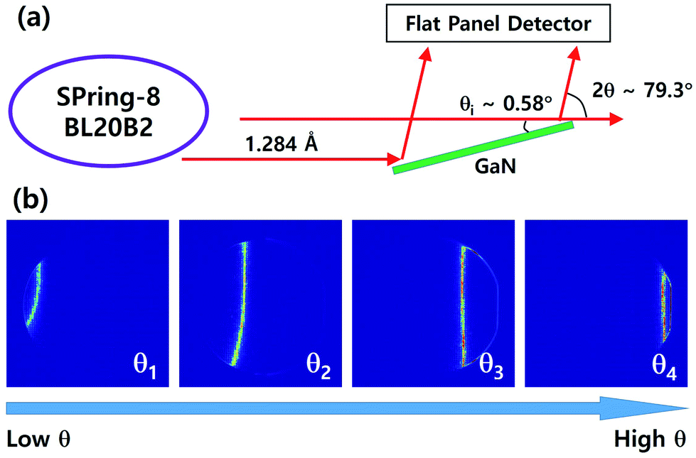 | ||
| Fig. 1 (a) Experimental setup for X-ray diffraction topography of GaN (114). We adjusted the incidence angle of the X-rays to ∼0.58° and installed a two-dimensional flat panel detector with a 2θ angle of 79.3°. (b) Partially diffracted X-rays at various incidence angles due to lattice plane bending are recorded. | ||
3 Results and discussion
We performed the same measurement procedures for the structural analysis of a 5 μm-thick homoepitaxial layer grown by metal–organic chemical vapor deposition. Fig. 2(a) and (c) show maximum intensity maps of the 2 inch GaN wafer before and after deposition of a 5 μm n-GaN homoepitaxial layer. The overall intensity decreased, and in particular, the lower left part of the wafer showed a drastic decrease in intensity. The FWHM maps evaluated from the peak widths before and after homoepitaxial layer deposition are shown in Fig. 2(b) and (d), respectively. The FWHM increased after homoepitaxial layer deposition, particularly at the lower left part of the wafer. These results can be interpreted as a lower crystallinity of the epitaxial layer; however, the crystal quality of a homoepitaxial layer is usually higher than that of bulk GaN crystals. | ||
| Fig. 2 Reconstructed wafer images from the (a) maximum intensity and (b) peak FWHM of the bulk substrate before the deposition of the homoepitaxial layer. After deposition of the homoepitaxial layer, the maximum intensity and FWHM values changed, as shown in (c) and (d), respectively. In particular, the lower left side of the wafer showed a decrease in intensity and increase in FWHM. | ||
To understand this interesting feature, we evaluated the bending angle maps shown in Fig. 3(a) and (b). The wafer exhibited convex bending, and there were almost no changes in the bending angles before and after deposition of the homoepitaxial layer. The line profiles shown in Fig. 3(c) and (d) also show no changes in wafer bending. We estimated the radius of curvature to be 9.5 m both before and after deposition. We attribute the lower intensities, wider FWHMs, and unchanged bending angles to sample miscut angle changes after the homoepitaxial layer deposition that affects the X-ray penetration.
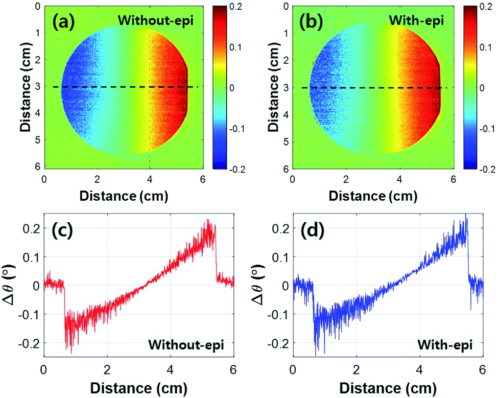 | ||
| Fig. 3 Reconstructed wafer bending-angle maps (a) before and (b) after the homoepitaxial layer deposition. Profiles along the dotted lines in (a) and (b) are shown in (c) and (d), respectively. The bending angle did not change after the homoepitaxial layer deposition. | ||
The index of refraction n for X-rays can be written as
| n = 1 − δ − iβ, | (1) |
![[small rho, Greek, macron]](https://www.rsc.org/images/entities/i_char_e0d1.gif) ere/2π and β = μ/2k. Here, e, re, μ, and k are the average electron number density, classical electron radius (whose value is 2.82 × 10⁻⁵ Å), absorption coefficient, and wavevector, respectively. The values of δ and β used for the calculations were 6.96 × 10⁻⁶ and 5.58 × 10⁻⁷, respectively, at the wavelength of 1.284 Å corresponding to a GaN electron number density of 1.66/Å3. The kinematic scattering intensity near total external reflection21–23 can be expressed as
ere/2π and β = μ/2k. Here, e, re, μ, and k are the average electron number density, classical electron radius (whose value is 2.82 × 10⁻⁵ Å), absorption coefficient, and wavevector, respectively. The values of δ and β used for the calculations were 6.96 × 10⁻⁶ and 5.58 × 10⁻⁷, respectively, at the wavelength of 1.284 Å corresponding to a GaN electron number density of 1.66/Å3. The kinematic scattering intensity near total external reflection21–23 can be expressed as| I(Q) ∝ |Ti|2S(Q)|Tf|2, | (2) |
 | (3) |
 | (4) |
 | (5) |
li,f = 2−1/2{(2δ − sin2![[thin space (1/6-em)]](https://www.rsc.org/images/entities/char_2009.gif) αi,f) + [(sin2αi,f − 2δ)2 + (2β)2]1/2}1/2. αi,f) + [(sin2αi,f − 2δ)2 + (2β)2]1/2}1/2.
| (6) |
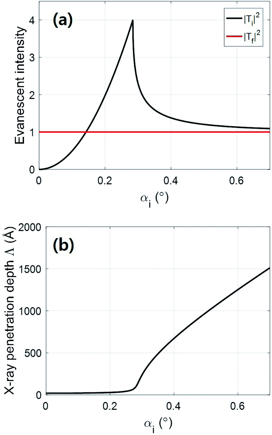 | ||
| Fig. 4 Theoretical calculations of the (a) evanescent intensities and (b) X-ray penetration depth Λ. The maximum evanescent intensity of |Ti|2 occurs at the critical incidence angle of the X-rays and then undergoes exponential damping while |Tf|2 is almost constant. The X-ray penetration depth tends to increase as the incidence angle of the X-rays increases. | ||
A theoretical calculation of the X-ray penetration depth is shown in Fig. 4(b); it starts to increase around 0.284°. The Λ at the critical angle was calculated to be 116 Å. As αi increases, Λ becomes linearly proportional to αi. The profiles of the X-ray diffraction peak of the GaN (114) are shown in Fig. 5(a), as calculated from eqn (2). The calculation results show that the diffraction intensity increases with αi. In addition, the peaks become sharper as αi increases, as shown in Fig. 5(b). This means that at low X-ray incidence angles, the sample volume that participates in the diffraction is small; more precisely, the number of unit cells along the surface normal is small. Thus, the low-angle X-ray intensity contains surface information. On the other hand, when the X-ray incidence angle is much larger than the critical angle, the diffraction peak is intense and sharp owing to the large X-ray penetration depth. In this case, the number of unit cells contributing to the X-ray diffraction is greater than that at low incidence angles. This enhances the diffraction intensity and makes the peak sharp.
 | ||
| Fig. 5 (a) Theoretical diffraction peak profiles as functions of qz and (b) FWHM vs. X-ray incidence angle. As the incidence angle decreases, the diffraction peak becomes broader and weaker. | ||
According to Hirai et al.,24 a surface hillock structure comprising m-plane GaN can be controlled by adjusting the miscut angles. In that report, a homoepitaxial layer grown on a GaN substrate with a miscut angle of 5.4° showed a smooth surface morphology. Furthermore, they found that the apex of a pyramidal hillock was related to the origin of a dislocation.25 For c-plane GaN, the hillock density decreased as the miscut angle increased toward the [10![[1 with combining macron]](https://www.rsc.org/images/entities/char_0031_0304.gif) 0] direction.26 The miscut angle in our 2 inch GaN was 0.4° smaller than in previous reports; however, we can expect the homoepitaxial layer to have a smoother surface. In our experiment, we observed the spread Δθ of the Bragg peak, instead of 2θ or qz, because we employed a two-dimensional detector and large X-ray beam. In principle, the value of Δθ should be half of Δ2θ, so we can interpret the broadening of Δθ as the broadening of Δ2θ.
0] direction.26 The miscut angle in our 2 inch GaN was 0.4° smaller than in previous reports; however, we can expect the homoepitaxial layer to have a smoother surface. In our experiment, we observed the spread Δθ of the Bragg peak, instead of 2θ or qz, because we employed a two-dimensional detector and large X-ray beam. In principle, the value of Δθ should be half of Δ2θ, so we can interpret the broadening of Δθ as the broadening of Δ2θ.
Fig. 6 shows a proposed model that is in accordance with experimental results, theoretical calculations, and previous reports. The deposition of a homoepitaxial layer on top of a freestanding GaN wafer enhances the surface flatness, as shown in Fig. 6(b), which decreases the X-ray incidence angle. This decreases the number of scattering atoms, which decreases the diffraction intensity and increases the peak width. However, the peak position does not change, because the wafer bending remains the same. Although we did not directly measure the X-ray reflectivity under this condition, we expect it to increase. Atomic force microscopy or related techniques can resolve very small areas that are suitable for understanding microstructures. The observation of a macroscopic morphology change, such as a change in hillock structure, using these techniques is difficult because the detected area is too small. Although destructive methods such as transmission electron microscopy and an alpha step exist, it is difficult to understand surface morphology changes and their relation with lattice planes directly.
 | ||
| Fig. 6 Proposed models to represent the surface morphology (a) before and (b) after homoepitaxial layer deposition. The incidence angle of the X-rays with respect to the surface decreases, reducing the X-ray penetration. Accordingly, the X-ray intensity decreases and the FWHM increases, while the bending angle remains unchanged. | ||
We believe that a combination of X-ray diffraction topography with surface X-ray diffraction, such as skew-angle X-ray diffraction,27 grazing-incidence asymmetric Bragg diffraction,28 and anomalous fine structure diffraction,29 can be used to understand the surface changes in homoepitaxial films.
4 Conclusion
In conclusion, we have observed the surface morphology smoothing of a 2 inch-diameter, bulk GaN wafer after the deposition of a homoepitaxial layer. The X-ray diffraction topography obtained from GaN (114) showed a decrease in X-ray intensity and increase in FWHM, while the bending angle did not change, after homoepitaxial layer deposition. Theoretical DWBA calculations show that the X-ray penetration depth decreases owing to the decreasing incidence angle of the X-rays. Accordingly, the number of atoms participating in the X-ray diffraction decreased, generating a weaker and wider diffraction peak. We believe that our approach will be useful for understanding the crystal quality of GaN homoepitaxial layers and bulk GaN.
Conflicts of interest
There are no conflicts of interest to declare.Acknowledgements
The measurements were performed at SPring-8 under proposal No. 2017B1029 and 2018B1010. This work was supported by the Ministry of Education, Culture, Sports, Science, and Technology (MEXT) “Program for Research and Development of Next-Generation Semiconductor to Realize Energy-Saving Society” and Basic Science Research Program through the National Research Foundation of Korea (NRF) funded by the Ministry of Education (Grant No. 2018R1A6A3A03012052).References
- H. Amano, M. Kito, K. Hiramatsu and I. Akasaki, Jpn. J. Appl. Phys., 1989, 28, L2112–L2114 CrossRef CAS
.
- S. Nakamura, T. Mukai, M. Senoh and N. Iwasa, Jpn. J. Appl. Phys., 1992, 31, L139–L142 CrossRef CAS
- Y. Wu, D. Kapolnek, J. P. Ibbetson, P. Parikh, B. P. Keller and U. K. Mishra, IEEE Trans. Electron Devices, 2001, 48, 586–590 CrossRef CAS
- W. Saito, Y. Takada, M. Kuraguchi, K. Tsuda, I. Omura, T. Ogura and H. Ohashi, IEEE Trans. Electron Devices, 2003, 50, 2528–2531 CrossRef CAS
- T. Palacios, A. Chakraborty, S. Heikman, S. Keller, S. P. DenBaars and U. K. Mishra, IEEE Electron Device Lett., 2006, 27, 13–15 CAS
- S. Kikuta, K. Kohra and Y. Sugita, Jpn. J. Appl. Phys., 1966, 5, 1047–1055 CrossRef CAS
- K. Motoki, T. Okahisa, S. Nakahata, N. Matsumoto, H. Kimura, H. Kasai, K. Takemoto, K. Uematsu, M. Ueno, Y. Kumagai, A. Koukitu and H. Seki, J. Cryst. Growth, 2002, 237–239, 912–921 CrossRef CAS
- R. Dwilinśki, R. Doradzinśki, J. Garczynśki, L. P. Sierzputowski, A. Puchalski, Y. Kanbara, K. Yagi, H. Minakuchi and H. Hayashi, J. Cryst. Growth, 2008, 310, 3911–3916 CrossRef
- R. Dwilinśki, R. Doradzinśki, J. Garczynśki, L. P. Sierzputowski, A. Puchalski, Y. Kanbara, K. Yagi, H. Minakuchi and H. Hayashi, J. Cryst. Growth, 2009, 311, 3015–3018 CrossRef
- B. C. Larson, W. Yang, G. E. Ice, J. D. Budai and J. Z. Tischler, Nature, 2002, 415, 887–890 CrossRef CAS PubMed
- W. Liu, G. E. Ice, B. C. Larson, W. Yang, J. Z. Tischler and J. D. Budai, Metall. Mater. Trans. A, 2004, 35, 1964–1967 Search PubMed
- G. E. Ice and B. C. Larson, Adv. Eng. Mater., 2000, 2, 643–646 CrossRef CAS
- L. Margulies, G. Winther and H. F. Poulsen, Science, 2001, 291, 2392–2394 CrossRef CAS
- R. Barabash, G. E. Ice, B. C. Larson, G. M. Pharr, K. S. Chung and W. Yang, Appl. Phys. Lett., 2001, 79, 749–751 CrossRef CAS
- W. M. Chen, P. J. McNally, K. Jacobs, T. Tuomi, A. N. Danilewsky, Z. R. Zytkiewicz, D. Lowney, J. Kanatharana, L. Knuuttila and J. Riikonen, J. Cryst. Growth, 2002, 243, 94–102 CrossRef CAS
- P. Tafforeau, R. boistel, E. Boller, A. Bravin, M. Brunet, Y. Chaimanee, P. Cloetens, M. Feist, J. Hoszowska, J.-J. Jaeger, R. F. Kay, V. Lazzari, L. Marivaux, A. Nel, C. Nemoz, X. Thibault, P. Vignaud and S. Zabler, Appl. Phys. A, 2006, 83, 195–202 CrossRef CAS
- J. Kim, O. Seo, C. Song, S. Hiroi, Y. Chen, Y. Irokawa, T. Nabatame, Y. Koide and O. Sakata, Phys. Rev. Appl., 2019, 11, 024072 CrossRef CAS
- J. Kim, O. Seo, C. Song, S. Hiroi, Y. Chen, Y. Irokawa, T. Nabatame, Y. Koide and O. Sakata, Appl. Phys. Express, 2018, 11, 081002 CrossRef
- J. Kim, O. Seo, C. Song, Y. Chen, S. Hiroi, Y. Irokawa, T. Nabatame, Y. Koide and O. Sakata, CrystEngComm, 2018, 20, 7761–7765 RSC
- J. Kim, O. Seo, C. Song, Y. Chen, S. Hiroi, Y. Irokawa, T. Nabatame, Y. Koide and O. Sakata, CrystEngComm, 2019, 21, 4036–4041 RSC
- G. H. Vineyard, Phys. Rev. B: Condens. Matter Mater. Phys., 1982, 26, 4146–4159 CrossRef CAS
- H. Dosch, Phys. Rev. B: Condens. Matter Mater. Phys., 1987, 35, 2137–2143 CrossRef CAS
- R. Feidenhans'l, Surf. Sci. Rep., 1989, 10, 105–188 CrossRef
- A. Hirai, Z. Jia, M. C. Schmidt, R. M. Farrell, S. P. DenBaars, S. Nakamura, J. S. Speck and K. Fujito, Appl. Phys. Lett., 2007, 91, 191906 CrossRef
- R. M. Farrell, D. A. Haeger, X. Chen, C. S. Gallinat, R. W. Davis, M. Cornish, K. Fujito, S. Keller, S. P. DenBaars, S. Nakamura and J. S. Speck, Appl. Phys. Lett., 2010, 96, 231907 CrossRef
- A. R. A. Zauner, J. L. Weyher, M. Plomp, V. Kirilyuk, I. Grzegory, W. J. P. van Enckevort, J. J. Schermer, P. R. Hageman and P. K. Larsen, J. Cryst. Growth, 2000, 210, 435–443 CrossRef CAS
- A. Reiher, J. Bläsing, A. Dadgar and A. Krost, Appl. Phys. Lett., 2004, 84, 3537–3539 CrossRef CAS
- M. F. Toney and S. Brennan, Appl. Phys. Lett., 1988, 65, 4763–4768 Search PubMed
- H. Stragier, J. O. Cross, J. J. Rehr, L. B. Sorensen, C. E. Bouldin and J. C. Woicik, Phys. Rev. Lett., 1992, 69, 3064–3067 CrossRef CAS
| This journal is © The Royal Society of Chemistry 2020 |