DOI:
10.1039/C9RA08836A
(Paper)
RSC Adv., 2020,
10, 4414-4426
An assessment on crystallization phenomena of Si in Al/a-Si thin films via thermal annealing and ion irradiation
Received
28th October 2019
, Accepted 14th January 2020
First published on 27th January 2020
Abstract
In the present study, crystallization of amorphous-Si (a-Si) in Al/a-Si bilayer thin films under thermal annealing and ion irradiation has been investigated for future solar energy materials applications. In particular, the effect of thickness ratio (e.g. in Al![[thin space (1/6-em)]](https://www.rsc.org/images/entities/char_2009.gif) :a-Si, the ratio of the Al and a-Si layer thickness) and temperature during irradiation on crystallization of the Si films has been explored for the first time. Two sets of samples with thickness ratio 1:1 (set-A: 50 nm Al/50 nm a-Si) and thickness ratio 1:3 (set-B: 50 nm Al/150 nm a-Si) have been prepared on thermally oxidized Si-substrates. In one experiment, thermal annealing of the as-prepared sample (of both the sets) has been done at different temperatures of 100 °C, 200 °C, 300 °C, 400 °C, and 500 °C. Significant crystallization was found to initiate at 200 °C with the help of thermal annealing, which increased further by increasing the temperature. In another experiment, ion irradiation on both sets of samples has been carried out at 100 °C and 200 °C using 100 MeV Ni7+ ions with fluences of 1 × 10¹² ions per cm2, 5 × 10¹² ions per cm2, 1 × 10¹³ ions per cm2, and 5 × 10¹³ ions per cm2. Significant crystallization of Si was observed at a remarkably low temperature of 100 °C under ion irradiation. The samples irradiated at 100 °C show better crystallization than the samples irradiated at 200 °C. The maximum crystallization of a-Si has been observed at a fluence of 1 × 10¹² ions per cm2, which was found to decrease with increasing ion fluence at both temperatures (i.e. 100 °C & 200 °C). The crystallization of a-Si is found to be better for set-B samples as compared to set-A samples at all the fluences and irradiation temperatures. The present work is aimed at developing the understanding of the crystallization process, which may have significant advantages for designing crystalline layers at lower temperature using appropriate masks for irradiation at the desired location. The detailed mechanisms behind all the above observations are discussed in this paper.
:a-Si, the ratio of the Al and a-Si layer thickness) and temperature during irradiation on crystallization of the Si films has been explored for the first time. Two sets of samples with thickness ratio 1:1 (set-A: 50 nm Al/50 nm a-Si) and thickness ratio 1:3 (set-B: 50 nm Al/150 nm a-Si) have been prepared on thermally oxidized Si-substrates. In one experiment, thermal annealing of the as-prepared sample (of both the sets) has been done at different temperatures of 100 °C, 200 °C, 300 °C, 400 °C, and 500 °C. Significant crystallization was found to initiate at 200 °C with the help of thermal annealing, which increased further by increasing the temperature. In another experiment, ion irradiation on both sets of samples has been carried out at 100 °C and 200 °C using 100 MeV Ni7+ ions with fluences of 1 × 10¹² ions per cm2, 5 × 10¹² ions per cm2, 1 × 10¹³ ions per cm2, and 5 × 10¹³ ions per cm2. Significant crystallization of Si was observed at a remarkably low temperature of 100 °C under ion irradiation. The samples irradiated at 100 °C show better crystallization than the samples irradiated at 200 °C. The maximum crystallization of a-Si has been observed at a fluence of 1 × 10¹² ions per cm2, which was found to decrease with increasing ion fluence at both temperatures (i.e. 100 °C & 200 °C). The crystallization of a-Si is found to be better for set-B samples as compared to set-A samples at all the fluences and irradiation temperatures. The present work is aimed at developing the understanding of the crystallization process, which may have significant advantages for designing crystalline layers at lower temperature using appropriate masks for irradiation at the desired location. The detailed mechanisms behind all the above observations are discussed in this paper.
I. Introduction
Polycrystalline silicon (poly-Si) is an interesting material for electronic devices such as thin-film solar cells and thin-film transistors.1–4 The crystallization of amorphous-Si (a-Si) offers the opportunity for using low-temperature and low-cost substrates to reduce the overall cost of a solar cell. The need to produce low cost solar cells prompted the research community to devise ways and means to produce poly-Si via solid-phase crystallization (SPC) of a-Si.5,6 SPC by thermal annealing, however, suffers from long annealing times even when the annealing temperature is very high; for example, in the case of Si, this temperature is close to 600 °C.7 The crystallization temperature has been found to be significantly lower when the amorphous phase is put in intimate contact with crystalline metals such as Aluminum (Al), a process known as aluminum induced crystallization (AIC). Al is successful in bringing out the crystallization at very low temperature, as it is a post-transition metal, which constitutes a simple eutectic binary system with Si, and is not involved in the formation of any compound phases via AIC.8–26
The AIC process in various Al/a-Si systems has been extensively investigated in the last decade because of applications of poly-Si in low-temperature production of high-performance solar cells, flat-panel displays, and high-density data storage devices. Many groups investigated the impact of different parameters such as Al and Si layer thicknesses, layer orders, layer interface types, and Al to Si content ratios on the AIC process.12–22 These studies were aimed at lowering the crystallization temperature, shortening the annealing time required for the crystallization of a-Si layer, and for obtaining poly-Si thin films.9–23 Nast et al.9,27 studied the effect of Al layer thickness on the morphology of crystalline-silicon (c-Si). In their study, the AIC samples having a-Si layer one-half of the thickness of the Al layer were found to produce a porous structure and therefore, no continuous film was observed. However, in case of a thicker a-Si layer (as compared to the Al layer), a continuous c-Si layer was found on the substrate. For a-Si film thickness equal to or slightly higher than the Al film thickness, continuous c-Si films were produced.28 Therefore, in order to reduce the crystallization temperature, shorten the annealing time, and obtain good crystallinity of Si, swift heavy ion (SHI) irradiation is employed nowadays. SHI irradiation offers the advantage of short processing time and spatial selectivity of substrate (by focusing the beam size) with great precision (through ion dose) in order to modify materials in a desired fashion. Moreover, SHI has been extensively used as a unique tool for the modification materials properties, thin film surface nano-structuring, structural phase transformations, and atomic mixing at interface etc.29–35 Therefore, under SHI irradiation, the crystallization of amorphous semiconductor is possible in a controlled manner because of mixing due to diffusion of metal and free semiconductor atoms in the bulk as well as to the interface.33,36–39 In our recent publication,40 SHI irradiation process has been successfully demonstrated for the first time on the crystallization of Si in presence of Al at a very low temperature of 100 °C. However, the impact of different parameters such as thickness ratio of Al/a-Si bilayer system, temperatures during ion irradiation, and some others parameters on crystallization of Si in Al/a-Si thin film using ion irradiation is lacking.
In present paper, mainly the effects of thickness ratio of Al/a-Si thin films, temperatures (during thermal annealing and ion irradiation), and ion fluence on crystallization process of Si are presented. Two sets of samples with thickness ratios 1:1 (set-A: 50 nm Al/50 nm a-Si) and 1:3 (set-B: 50 nm Al/150 nm a-Si) were prepared on thermally oxidized Si-substrates. The ion irradiation was carried out with 100 MeV Ni7+ ions at 100 °C and 200 °C with different fluences of 1 × 10¹² ions per cm2, 5 × 10¹² ions per cm2, 1 × 10¹³ ions per cm2, and 5 × 10¹³ ions per cm2. In order to critically compare the role of swift heavy ions and annealing in crystallization, another set of both the samples was thermally annealed at different temperatures of 100 °C, 200 °C, 300 °C, 400 °C, and 500 °C. The detail mechanism and effect of thickness ratio of Al/a-Si bilayer system, annealing temperatures and fluence on crystallization of a-Si have thoroughly been discussed.
In Section II, we present the experimental details followed by Section III in which the results have been discussed. Conclusions have been drawn in Section IV.
II. Experimental methods
The 50 nm and 150 nm-thick a-Si films were grown on 500 nm thermally oxidized Si (100) substrate by means of electron beam evaporation in high vacuum chamber, with a base pressure of ∼10−7 mbar. In order to have metal/a-Si interface, 50 nm thin Al film was deposited on the top of the a-Si film using thermal evaporation method without disturbing the vacuum in the chamber. The bilayer films with configurations Al (50 nm)/a-Si (50 nm)/SiO2 (i.e. thickness ratio of Al/a-Si∼1:1, called set-A sample) and Al (50 nm)/a-Si (150 nm)/SiO2 (i.e. thickness ratio of Al/a-Si∼1:3, called set-B) were prepared. One set of both the bilayer films was annealed at different temperatures of 100 °C, 200 °C, 300 °C, 400 °C, and 500 °C in N2 ambient for two hours in tubular furnace with a ramp rate of 20 °C min−1. Another set of samples was irradiated by 100 MeV Ni7+ ions scanned uniformly on the sample in a high vacuum chamber (at the pressure of ∼1 × 10⁻⁶ mbar) at temperatures of 100 °C and 200 °C with different fluences of 1 × 10¹² ions per cm2, 5 × 10¹² ions per cm2, 1 × 10¹³ ions per cm2, and 5 × 10¹³ ions per cm2 using 15 UD Pelletron tandem accelerator facility of Inter University Accelerator Center (IUAC), New Delhi. The electronic stopping power (Se) and nuclear stopping power (Sn) values for 100 MeV Ni ions were calculated using SRIM simulation code,41 which were found to be 7.19 keV nm−1 and 0.013 keV nm−1 in Si and 8.27 keV nm−1 and 0.014 keV nm−1 in Al, respectively. In order to study crystallization, grazing incidence X-ray diffraction (GIXRD) was performed using D8 Bruker diffractometer with grazing incidence angle of 0.5° and scan rate of 2° min−1. The Raman spectra were recorded using a Renishaw microscope with 514 nm He–Ne laser excitation. The cross sectional transmission electron microscopy (XTEM) measurements were carried out using JEM F200 (JEOL) with 200 kV field emission gun. Transport and range of ions in matter (TRIM) simulations were performed to find out the target displacement due to ion irradiation.41 In order to understand the role of SHI irradiation on crystallization, the increase of lattice temperature during ion irradiation due to inelastic collisions was estimated using thermal spike calculation code.42
III. Results and discussions
A. AIC under thermal annealing
AIC under thermal annealing may be explained as follows. The grain boundaries in poly-crystalline Al act as nucleation sites which lead to the crystal growth. The Si atoms from a-Si side reach to these nucleation sites by short-ranged atomic transport. According to the classical nucleation theory,43 the rate of nucleation is proportional to  where ΔG is the free energy enthalpy for forming the surface of the expanding nucleus and the difference in bulk energy between the forming phase and the earlier phase. The formation of the c-Si phase is thermodynamically favorable as this process results in reduction of the overall free energy of the bilayer system. The subsequent growth of the c-Si nucleus occurs due to the arrival of more and more Si atoms to the c-Si nuclei. The growth of the c-Si phase is governed by Kolmogorov–Johnson–Mehl–Avrami (KJMA) theory,44,45 which relates the fraction of transformed crystalline phase (ftrans) to the annealing time (t):
| | |
ftrans = 1 − exp(−β(tn))
| (1) |
where β is Avrami constant and n is Avrami's growth exponent. Since the whole process of AIC involves inter-diffusion of Si and Al, this is also named layer exchange process.10–28
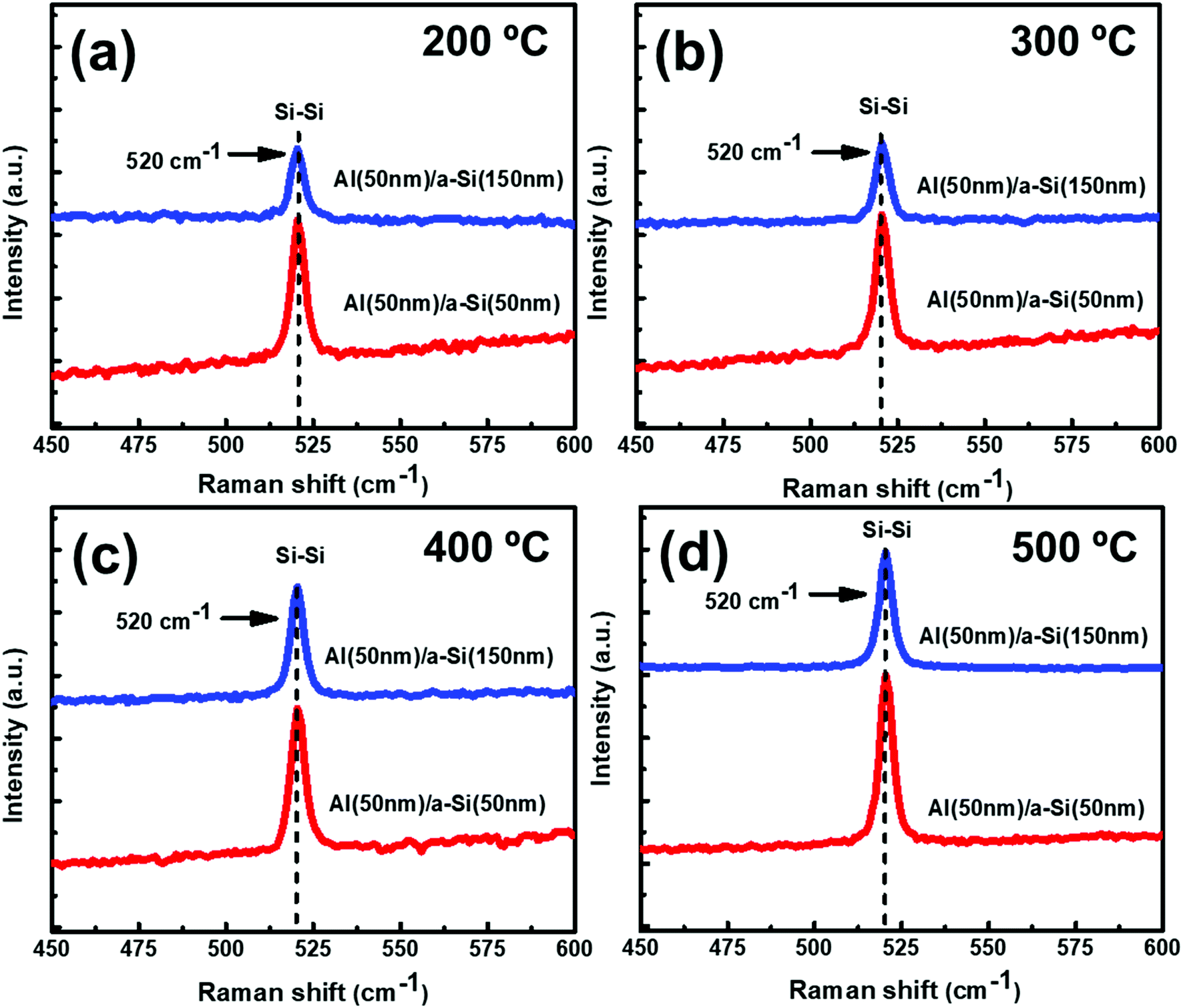
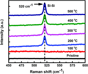
1. Effects of temperature. In order to understand the effect of temperature on crystallization of Si due to thermal annealing, both sets of the samples (set-A and set-B) have been annealed for two hours at different temperatures of 100 °C, 200 °C, 300 °C, 400 °C, and 500 °C. Fig. 1 shows the Raman spectra of set-A (Al:a-Si ∼ 1:1) samples. No Raman peak(s) corresponding to c-Si have been observed at 100 °C. However, as annealing temperature is increased to 200 °C and beyond, crystallization seems to start in the samples. The Raman peak at 520 cm−1 is assigned to the transverse optical (TO) mode of c-Si. The Raman peak intensity is found to increase with increase in the annealing temperature, showing an improvement in the crystallinity of Si. Exactly similar Raman results have been observed for set-B (Al:a-Si ∼ 1:3) samples as well. The crystalline volume fraction (Xc, which is similar to ftrans) has been deduced from the Raman spectra. There are several methods to determine Xc from the Raman spectra,46–51 apart from the analysis of polarization Raman scattering.52 In the present manuscript, we have adapted the method proposed by Okada et al.,48 in which the measured Raman spectra is resolved into crystalline and amorphous components and their integrated intensities are obtained as Ic and Ia. It is assumed that Ic and Ia represent the contributions from a crystalline component Xc and an amorphous component (1 − Xc) in the probed volume. The volume fraction of crystallinity is determined by the equation  where, α is the ratio of the integrated Raman cross-section for c-Si to a-Si, known as optical absorption correction factor,
  and
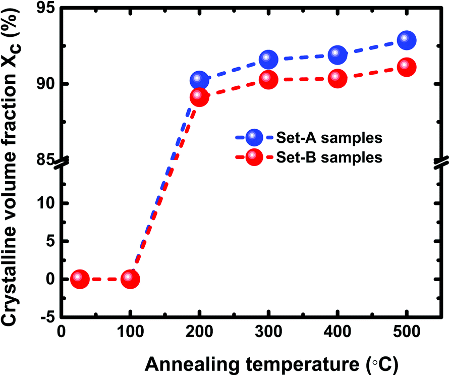
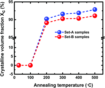
and  and Σ is the integrated cross-section over the resolved frequency range. To calculate Xc, the value of α has been taken as 0.8 from the literatures.47,50,51 This value of α is reasonable because the optical properties of the crystalline and amorphous phases are similar in a film coexistent with μc-Si and a-Si.48 Very recently, Jiang et al.51 used this method to determine Xc of Ge in Al-induced crystalline Ge system. Fig. 2 shows the calculated crystalline volume fraction of set-A and set-B samples annealed at different temperatures. The Xc values are found to be zero for the pristine sample and the sample annealed at 100 °C in both set of samples, which shows the absence of crystallization in the samples. The Xc value is found to be 90.22% when the samples are annealed at 200 °C; increasing the annealing temperatures further results in the increase in Xc value, which goes to 92.86% at 500 °C, for set-A samples. Similarly, the Xc value is found to be 89.12% when the samples are annealed at 200 °C; increasing the annealing temperatures further results in the increase in Xc value, which goes to 91.12% at 500 °C, for set-B samples.
 |
| | Fig. 1 Raman spectra of set-A (Al:a-Si ∼1:1), pristine sample and samples annealed at different temperatures of 100 °C, 200 °C, 300 °C, 400 °C, and 500 °C. | |
 |
| | Fig. 2 The Xc values of pristine and samples annealed at different temperatures of 100 °C, 200 °C, 300 °C, 400 °C, and 500 °C. | |
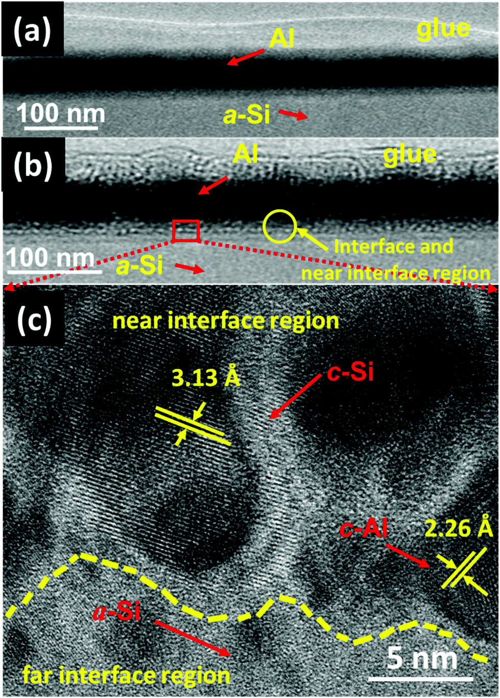
The GIXRD measurements have also been carried out on both set of (set-A and set-B) samples to get more insight into the crystallization of a-Si. The GIXRD pattern of pristine and annealed at different temperatures of 100 °C, 200 °C, 300 °C, 400 °C, and 500 °C for set-A samples is shown in Fig. 3. A single diffraction peak at 39.94° corresponding to Al (111) lattice plane is found for pristine sample. The sample annealed at 100 °C does not show any new diffraction peak corresponding to c-Si. When the sample annealing temperature was raised to 200 °C, a small diffraction peak of c-Si originating from (111) lattice plane18 was observed at about 28°. The diffraction peak intensity corresponding to c-Si is found to be increases further with the increase of annealing temperature from 300–500 °C, which confirms the increase of crystallinity with annealing temperature. Similar GIXRD results have also been observed for the set-B sample. Therefore, one can say that the GIXRD results are in agreement with the Raman results. In order to get further confirmation of crystallization, XTEM measurements have been carried out on pristine set-A sample and set-A sample annealed at 200 °C. The pristine set-A reflects sharp interface of Al and a-Si layer, as shown in Fig. 4(a). Fig. 4(b) shows the XTEM image of set-A sample annealed at 200 °C which clearly depicts the diffused interface due to diffusion of free a-Si atoms along the Al grain boundaries near to the interface region during thermal annealing. Fig. 4(c) shows the high-resolution TEM (HRTEM) image of a selected region of the interface which clearly reveals the crystallization of Si at 200 °C. The inter-planar spacing corresponding to c-Si and c-Al has been found to be 3.13 Å and 2.26 Å, respectively. It is also observed that the crystallization of Si at 200 °C occurs at the near interface region. It must be mentioned here that the thermal annealing at higher temperature (i.e. 500 °C) may lead to the crystallization of Si up to deep into the Al layer, as the atomic diffusion is faster at higher temperature. The nucleation and growth of the c-Si phase under thermal annealing condition can be understood on the basis of diffusion and sufficient availability of Si atoms along the Al grain boundaries at different temperatures.12–22,40 In present investigation, we have observed that the crystallization of a-Si is initiated at around 200 °C and the crystalline volume fraction increases further with increasing temperature up to 500 °C due to increased supply of Si atoms around Al grain boundaries from the underlying a-Si layer.12–22 These suggest that the diffusion of Si atoms in Al is activated at around 200 °C because of very high (many orders of magnitude) diffusion constant of Si in Al compared to the diffusion constant of Al in Si.53,54 The continuous diffusion, crystallization and grain growth of Si in Al builds compressive stress in the Al grains and tensile stress in the a-Si layer. As a result of both effect, Al tends to migrate into the underlying a-Si layer and eventually replace the whole Si layer, known as layer exchange mechanism.10–28 Therefore, the crystallization of Si for both set of samples (set-A & set-B) has been found at higher annealing temperature and found to increase with the increasing of annealing temperatures.
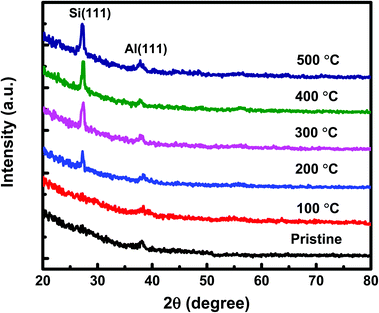 |
| | Fig. 3 The GIXRD patterns of set-A pristine sample and samples annealed at different temperatures of 100 °C, 200 °C, 300 °C, 400 °C, and 500 °C. | |
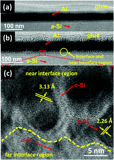 |
| | Fig. 4 (a) XTEM image of pristine set-A sample (b) XTEM image of set-A sample annealed at 200 °C (c) high resolution TEM (HRTEM) micrograph of set-A sample annealed at 200 °C. | |
2. Effects of thickness. In order to investigate the effects of thickness ratio on crystallization of a-Si, Raman spectra of set-A (i.e. thickness ratio 1:1) and set-B (i.e. thickness ratio 1:3) samples have been plotted in Fig. 5. Fig. 5(a) shows the Raman spectra for set-A and set-B samples annealed at 200 °C. The Raman peak intensity for the set-A samples with thickness ratio 1:1 is found to be higher than the set-B sample with thickness ratio 1:3. As annealing temperature of the samples is increased beyond 200 °C, the height of the corresponding intensity peaks is also found to increase, signaling the growth of the crystalline region (see Fig. 5(b–d)). It is also noted from Fig. 5 that the crystallization of a-Si is apparently better when the thickness ratio of the samples is 1:1 (set-A) as compared to the sample with the thickness ratio 1:3 (set-B). The crystalline volume fraction (Xc) for the sample with the thickness ratio 1:1 has been found to be 90.22% and for the sample with thickness ratio 1:3 is 89.12% when both the samples are annealed at 200 °C for the same time duration. This trend continues even at higher temperatures; for instance, at 500 °C, Xc is 92.86% for the sample with thickness ratio 1:1 and 91.12% for the sample with thickness ratio 1:3. This type of variation in crystalline volume fraction has also been reported by several other researchers.10,28,55,56 The main reason behind the lower crystallization in set-B sample in this annealing temperature range might be due to the lack of enough supply of Si atoms from the deeper Si layers due to its larger thickness. Therefore, due to annealing for a particular temperature and time the variation in crystalline volume fraction for set-A and set-B has been observed in XRD and Raman analyses.
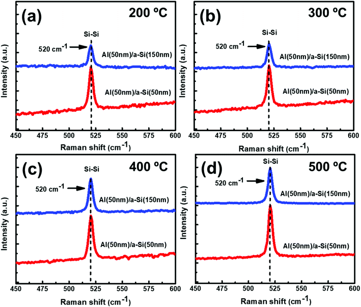 |
| | Fig. 5 The Raman spectra of set-A and set-B samples thermally annealed at different temperatures of (a) 200 °C, (b) 300 °C, (c) 400 °C, and (d) 500 °C. (All figures are plotted in same y-scale range for comparison). | |
B. AIC under ion irradiation
Under irradiation, atomic diffusion results in the transport of Si atoms across the interface. This results in an increase in the concentration of Si atoms at the nucleation sites. Increase in the Si concentration decreases the barrier for c-Si nucleation. This is why the crystallization of Si may observe even at low temperature during irradiation. The growth of c-Si happens due to arrival of Si atoms by atomic diffusion.
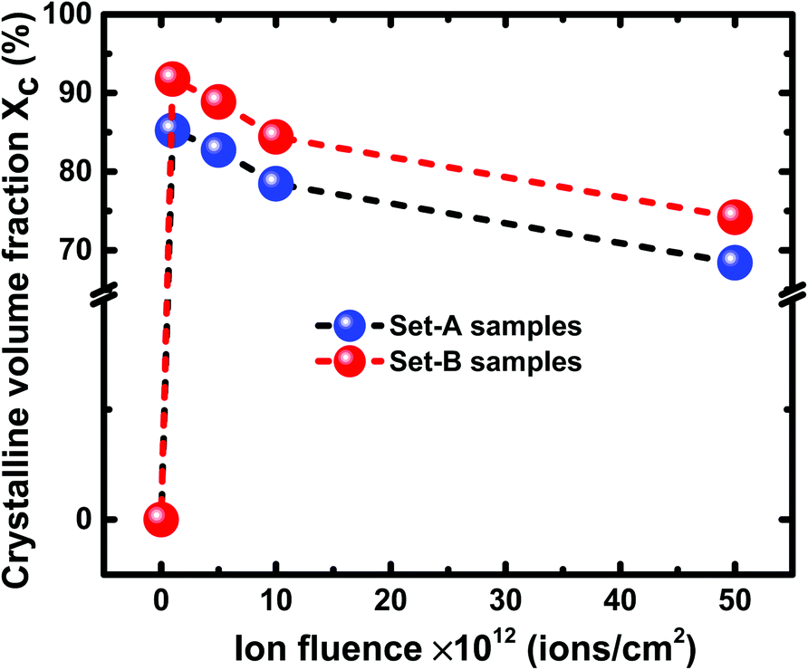
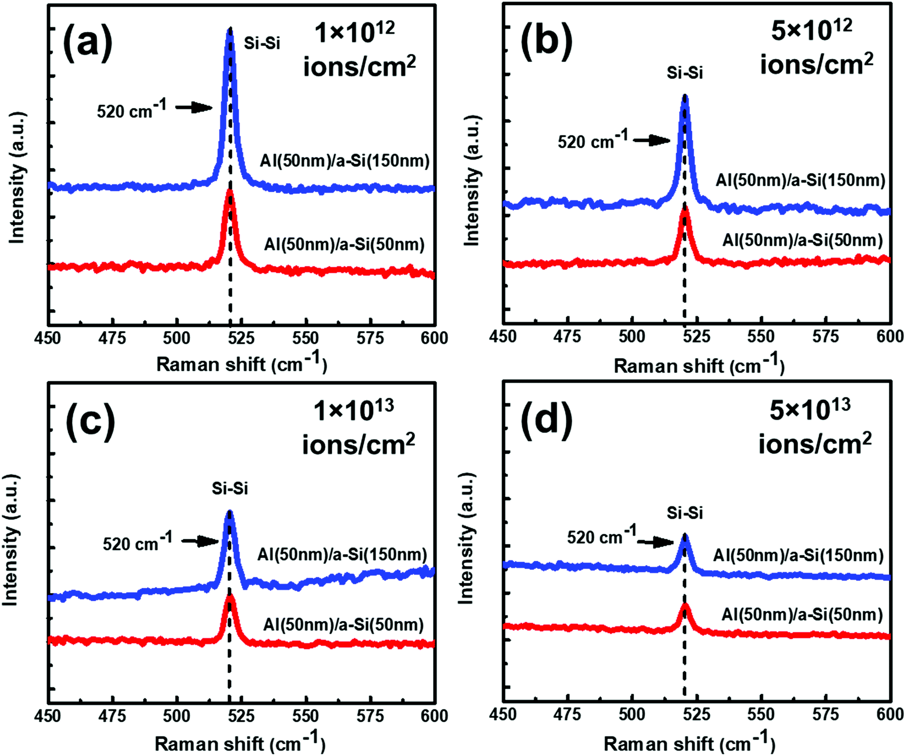
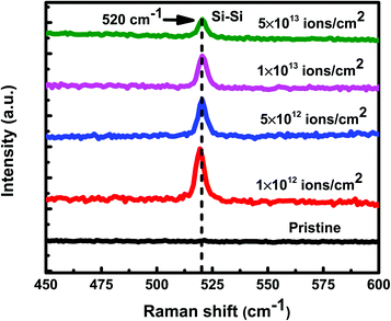
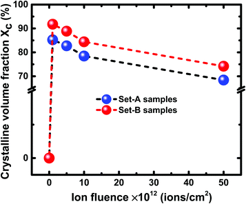
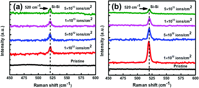
1. Effect of fluence. In order to reduce the crystallization temperature of Si, both sets of samples (set-A and set-B) have been exposed to ion beam irradiation at 100 °C with different fluences of 1 × 10¹² ions per cm2, 5 × 10¹² ions per cm2, 1 × 10¹³ ions per cm2, and 5 × 10¹³ ions per cm2. Fig. 6 shows the Raman spectra of set-A samples irradiated at temperature of 100 °C with different fluences of 1 × 10¹² ions per cm2, 5 × 10¹² ions per cm2, 1 × 10¹³ ions per cm2, and 5 × 10¹³ ions per cm2, with respect to the pristine sample. The pristine samples of both the sets do not show any Raman peak, which confirms the amorphous nature of Si. A Raman peak at 520 cm−1 is observed in the samples when they were irradiated with different fluences at temperature of 100 °C. The Raman peak at 520 cm−1 corresponds to transverse optical (TO) phonon mode of c-Si. The Raman peak intensity is found to decrease with increasing ion fluences, which reveals the decrease in the crystallinity at higher fluences due to disorder and radiation-induced amorphization.57 These observations are similar in both sets of the samples (set-A & set-B). The crystalline volume fraction (Xc) has been calculated from Raman spectra for both sets of the samples. Fig. 7 shows the Xc value of set-A and set-B samples irradiated at 100 °C with different fluences of 1 × 10¹² ions per cm2, 5 × 10¹² ions per cm2, 1 × 10¹³ ions per cm2, and 5 × 10¹³ ions per cm2. In set-A samples, Xc was found to decrease from 85.26% to 68.42% when fluence was varied from 1 × 10¹² ions per cm2 to 5 × 10¹³ ions per cm2. In set-B samples, the Xc values are found to decrease from 91.77% to 74.21% as the ion fluence increases from 1 × 10¹² ions per cm2 to 5 × 10¹³ ions per cm2.
 |
| | Fig. 6 Raman spectra of set-A samples irradiated at temperature of 100 °C with different fluences of 1 × 10¹² ions per cm2, 5 × 10¹² ions per cm2, 1 × 10¹³ ions per cm2, and 5 × 10¹³ ions per cm2. The Raman spectrum of pristine samples has also been displayed for comparison with irradiated samples. | |
 |
| | Fig. 7 The crystalline volume fraction (Xc) of set-A and set-B samples irradiated at 100 °C with different fluences of 1 × 10¹² ions per cm2, 5 × 10¹² ions per cm2, 1 × 10¹³ ions per cm2, and 5 × 10¹³ ions per cm2. | |
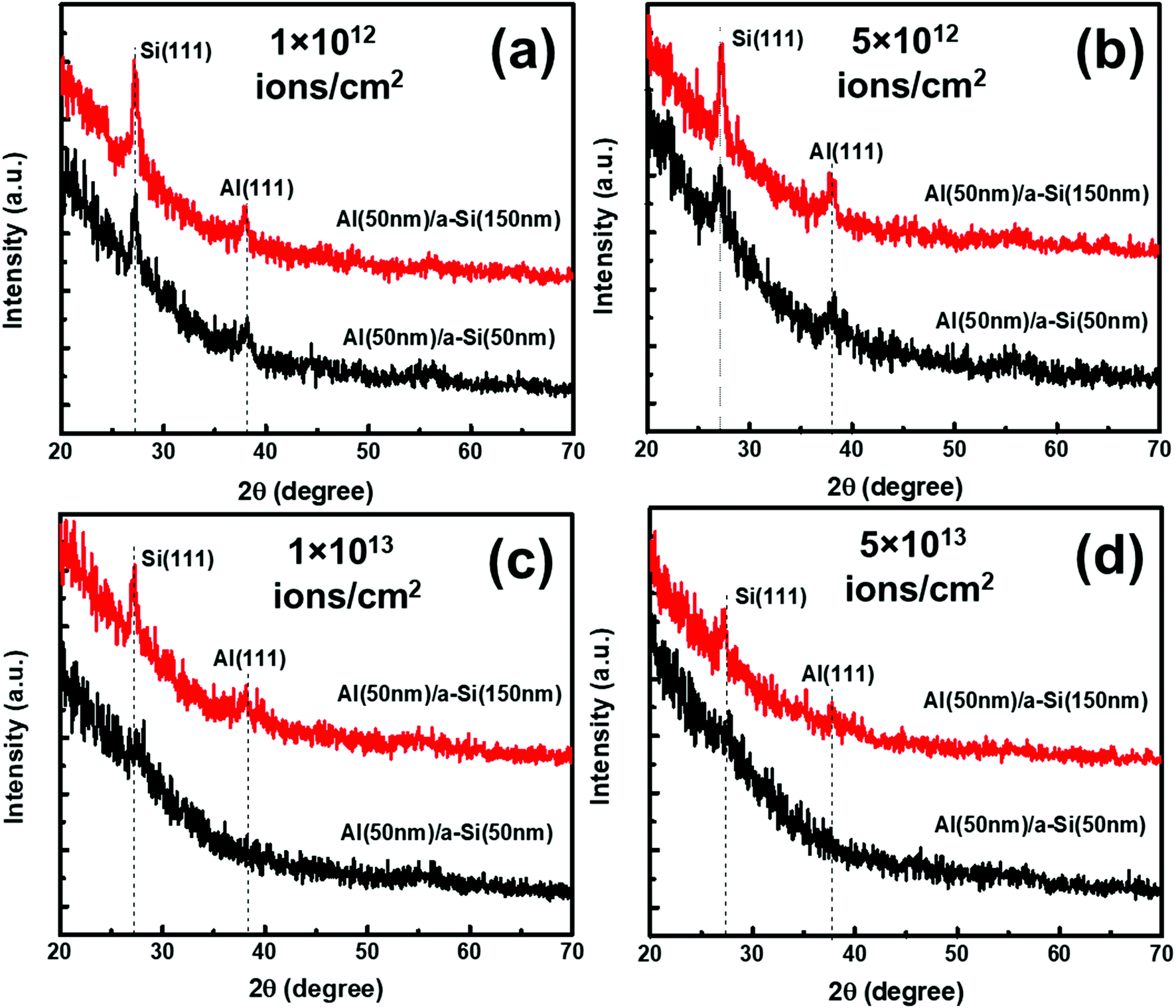
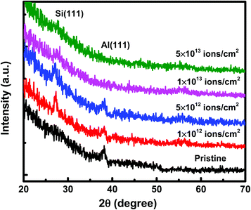
Further investigations on crystallization in both set of samples have been explored with the help of GIXRD measurements. Fig. 8 shows the GIXRD pattern of pristine and samples irradiated at 100 °C temperature with different fluences of 1 × 10¹² ions per cm2, 5 × 10¹² ions per cm2, 1 × 10¹³ ions per cm2, and 5 × 10¹³ ions per cm2 for set-A samples. The pristine sample of set-A shows a single diffraction peak, at 2θ of 39.94°, which corresponds to Al (111) lattice plane and no other diffraction peak corresponding to c-Si peaks were detected within the statistical limit of counts. However, after ion irradiation at 100 °C, two diffraction peaks are visible at 2θ about 28° and 39.94°, which are assigned to the diffraction from Si (111) and Al (111) lattice planes, respectively, which confirms the crystallization of a-Si.18 It is interesting to note that the c-Si (111) diffraction peak is highest at the lowest fluence, which decreases with increasing ion fluence. The decrease in silicon diffraction peak with increasing fluence reveals the amorphization of c-Si due to irradiation at higher fluence. Similar results have also been obtained for the set-B samples (with the thickness ratio of 1:3). The peak intensity of Al is also observed to decrease with increasing ion fluence. This observation reveals the amorphization of Al at higher fluence.58,59
 |
| | Fig. 8 GIXRD pattern of set-A pristine sample and samples irradiated with different fluences of 1 × 10¹² ions per cm2, 5 × 10¹² ions per cm2, 1 × 10¹³ ions per cm2, and 5 × 10¹³ ions per cm2 at temperature of 100 °C. | |
2. Effect of elevated temperature during irradiation. In order to study the effect of temperature during irradiation on crystallization of both set of the samples (with different thickness), we further performed ion irradiation experiments at a temperature of 200 °C. Fig. 9(a) and (b) show the Raman spectra of set-A and set-B samples respectively, irradiated at 200 °C with different fluences. The Raman peak intensity for both set of samples is found to decrease with increase in the ion fluence (similar as in case of sample irradiated at temperature of 100 °C). Fig. 9 gives a comparative perspective on crystallization in both the set of samples when the temperature during irradiation was raised to 200 °C. We see that crystallization in set-A samples is sluggish as compared to set-B samples under these conditions.
 |
| | Fig. 9 Raman spectra of (a) set-A and (b) set-B samples, irradiated at 200 °C with the different fluences of 1 × 10¹² ions per cm2, 5 × 10¹² ions per cm2, 1 × 10¹³ ions per cm2, and 5 × 10¹³ ions per cm2 with respect to pristine. | |
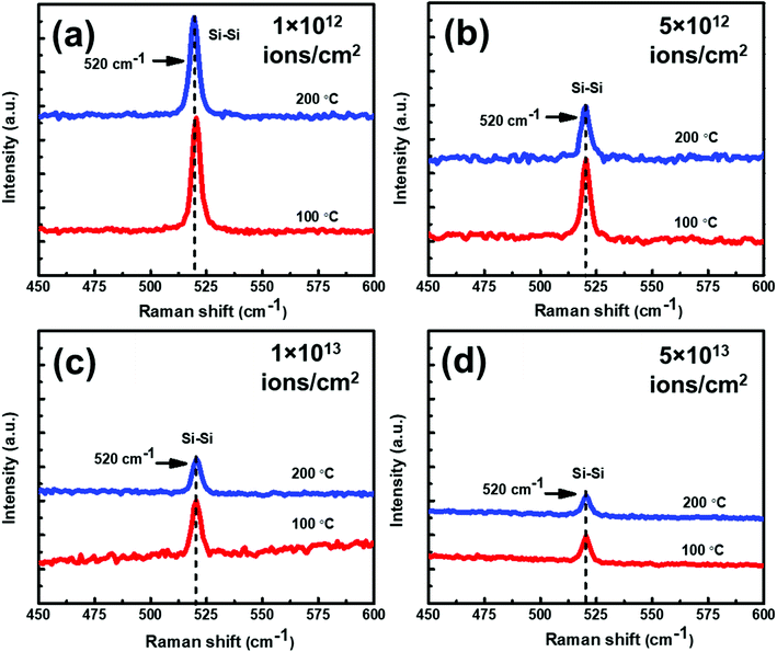
In order to understand the effect of temperature on the samples under irradiation, Raman spectra of set-B samples have been displayed in Fig. 10(a–d). In this figure, Raman spectra of set-B samples irradiated at 100 °C and 200 °C with different fluences have been shown.
 |
| | Fig. 10 Raman spectra of set-B sample irradiated at 100 °C and 200 °C with the different fluences of (a) 1 × 10¹² ions per cm2, (b) 5 × 10¹² ions per cm2, (c) 1 × 10¹³ ions per cm2, and (d) 5 × 10¹³ ions per cm2. (All figures are plotted in same y-scale range for comparison). | |
From Fig. 10, it is evident that at all the fluences, the Raman intensity peak corresponding to c-Si is always higher at 100 °C than at 200 °C. In other words, irrespective of the irradiation fluence, the crystallinity is always better in the samples irradiated at 100 °C as compared to the samples irradiated at higher temperatures. The Raman results of the set-A samples follow similar trend as those of set-B samples. The crystalline volume fraction (Xc) of set-B samples irradiated with a fluence of 1 × 10¹² ions per cm2 at 100 °C and 200 °C has been found to be 91.77% and 90.53%, respectively. The crystalline volume fraction (Xc) has also been calculated at 100 °C and 200 °C for a higher fluence of 5 × 10¹³ ions per cm2; the Xc values were found to be 74.21% and 69.07%, respectively corresponding to the temperatures of 100 °C and 200 °C. Similarly, the crystalline volume fraction (Xc) of set-A samples irradiated with a fluence of 1 × 10¹² ions per cm2 at 100 °C and 200 °C has been found to be 85.26% and 54.69%, respectively. At a higher fluence of 5 × 10¹³ ions per cm2, the crystalline volume fraction (Xc) values were found to be 68.42% and 45.31%, respectively, corresponding to 100 °C and 200 °C temperatures, confirming the consistent trend of decreasing crystallinity of irradiated samples at higher temperatures, irrespective of the fluence. The all Xc values of set-A and set-B irradiated with 100 °C and 200 °C are summarized in Table 1.
Table 1 The crystalline volume fractions of set-A and set-B irradiated with different temperatures
| Ion fluence |
Crystalline volume fraction of set-A (%) |
Crystalline volume fraction of set-B (%) |
| 100 °C |
200 °C |
100 °C |
200 °C |
| 1 × 10¹² ions per cm2 |
85.26 |
54.69 |
91.77 |
90.53 |
| 5 × 10¹² ions per cm2 |
82.75 |
51.80 |
88.85 |
87.01 |
| 1 × 10¹³ ions per cm2 |
78.46 |
49.15 |
84.41 |
82.39 |
| 5 × 10¹³ ions per cm2 |
68.42 |
45.31 |
74.21 |
69.07 |
3. Effect of thickness ratio. In order to study the effect of thickness ratio on crystallization in the samples irradiated at 100 °C, Raman spectra of both set of samples were recorded under the same laser excitation (see Fig. 11(a–d)). At all the fluences, the Raman peak intensities for the irradiated samples with thickness ratio 1:1 are observed to be lower than the samples with the thickness ratio 1:3. Therefore, contrary to thermally annealed samples, irradiated samples with thickness ratio of 1:3 seem to show better crystallization than the samples with thickness ratio 1:1.
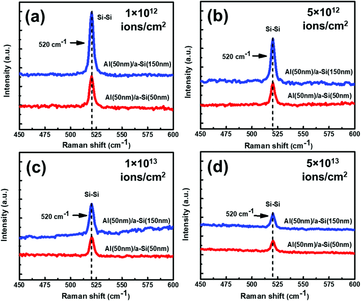 |
| | Fig. 11 Raman spectra of set-A and set-B samples irradiated at 100 °C with different fluences of (a) 1 × 10¹² ions per cm2, (b) 5 × 10¹² ions per cm2, (c) 1 × 10¹³ ions per cm2, and (d) 5 × 10¹³ ions per cm2. (All figures are plotted in same y-scale range for comparison). | |
The effect of thickness on crystallization of Si has also been investigated with the help of GIXRD measurement and shown in Fig. 12(a–d). In Fig. 12(a–d), two diffraction peaks are visible at 2θ about 28° and 39.94° which correspond to diffractions from Si (111) and Al (111), lattice planes, respectively. The diffraction peak intensities for the samples with thickness ratio 1:1 are found to be smaller than the samples with thickness ratio 1:3. This result depicts that the growth of c-Si along the direction of (111) is favorable in the samples with thickness ratio 1:3 at all the fluences. We also see reduction in the Raman peak intensities as the fluence increases.
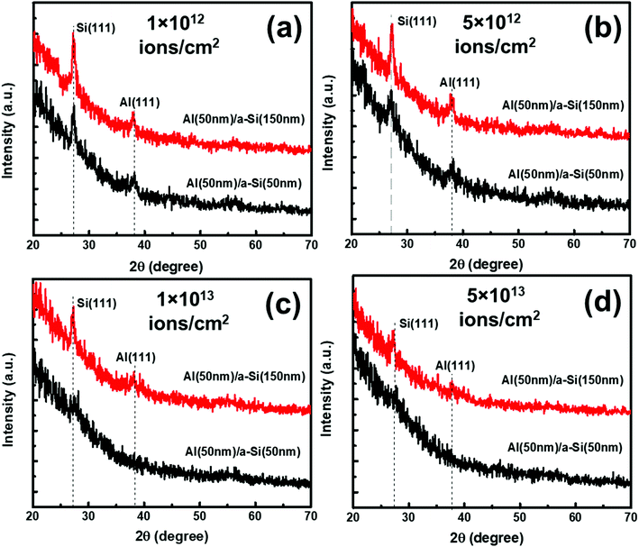 |
| | Fig. 12 GIXRD pattern shows the effect of thickness ratio in crystallization due to ion beam irradiation with different fluences of (a) 1 × 10¹² ions per cm2, (b) 5 × 10¹² ions per cm2, (c) 1 × 10¹³ ions per cm2, and (d) 5 × 10¹³ ions per cm2, at temperature of 100 °C. (All figures are plotted in same y-scale range for comparison). | |
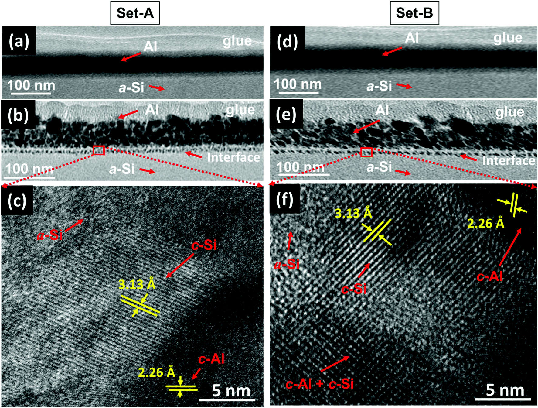
In order to confirm the crystallization of a-Si at a temperature of 100 °C under SHI irradiation further, XTEM measurements of both sets of pristine and samples irradiated at a fluence of 5 × 10¹² ions per cm2 were carried out, which have been shown in Fig. 13(a–f). Fig. 13(a) and (d) show the XTEM micrograph of pristine samples of set-A and set-B, respectively. The layers are distinct and there is no sign of interface diffusion (i.e. almost sharp interface) in both the sets of pristine samples. Fig. 13(b) and (e) clearly depict that the ion beam irradiation leads to diffused interface in both the sets of samples. The atomic transport via mixing from both the sides of the interface might be the possible cause for the diffused interface.60 Fig. 13(c) and (f) show high-resolution TEM (HRTEM) images of a selected region of the interface (for the both sets of samples), which clearly shows crystallization of a-Si. The inter-planar spacing corresponding to c-Si and c-Al (in both the sets of samples) has been found to be 3.13 Å and 2.26 Å, respectively. In the case of set-B samples (Fig. 13(f)), the crystallization of a-Si is observed to occur near the interface region; a mixture of c-Si and c-Al phases has also been observed at various places near the interface. Although, the crystallization in both types of the samples (set-A and set-B) is observed to happen at the interface, the details of the crystallization are a bit different: in the case of set-B sample, most of the portion at the interface is crystalline, whereas most of the portion is amorphous in the case of set-A samples.
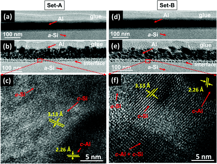 |
| | Fig. 13 XTEM and high resolution TEM (HRTEM) micrograph of both bilayer system (set-A & set-B) with pristine and irradiated with 5 × 10¹² ions per cm2 at temperature of 100 °C. For the set-A sample (a) XTEM image of pristine sample (b) XTEM image of irradiated sample (c) HRTEM image of the interface for irradiated sample. For the set-B sample (d) XTEM image of pristine (e) XTEM image of irradiated sample (f) HRTEM image of the interface for irradiated sample. | |
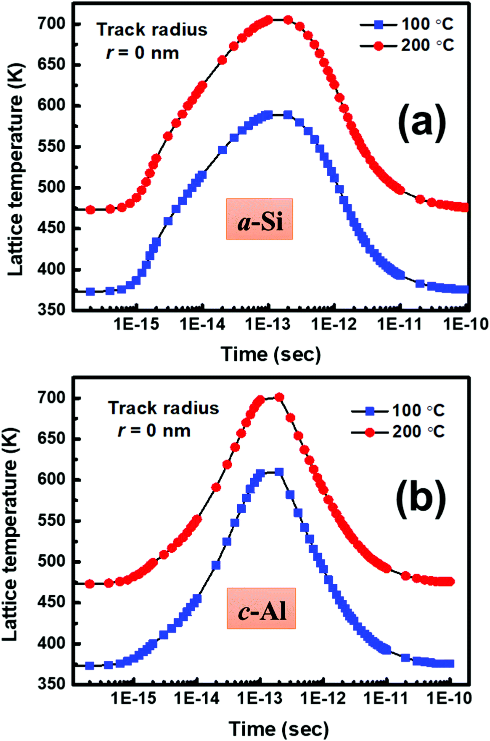
Our investigation clearly indicates that the SHI irradiation leads to the crystallization of a-Si in contact with c-Al at significantly low temperatures (as compared to the annealing temperature). In order to understand the possible mechanism of crystallization at a-Si/c-Al interface, let us first discuss the interaction of SHI with materials. When an energetic ion penetrates through a material, it loses energy through inelastic collisions with the target electrons (i.e. electronic energy loss) and elastic collision with nucleus of the target (i.e. nuclear energy loss).61 In the low energy regime, nuclear energy loss (Sn) results in atomic displacements, which ultimately results in generation of residual proportional of point defects/defect clusters in the crystalline solids. The electronic excitation/ionization leads to the sudden rise of the temperature in the cylindrical zone along the ion track, and creates local agitation in the lattice. There are two theoretical models, namely Coulomb explosion and thermal spike,39,42 which are used to explain the local transient lattice temperature due to rapid energy transferred from highly excited electron system to the atom. According to the thermal spike model, the generated free electrons are confined within a narrow cylindrical target zone around the ion path called the ion track. The confinement of these electrons depends on electron diffusion length and thus modifies electron-phonon coupling (g). The coupling term ‘g’ governs the efficiency with which energy deposited in the electronic subsystem is subsequently transferred to the lattice sub-system per unit volume and the time to increase lattice temperature. In order to estimate the rise of local temperature due to ion irradiation, thermal spike calculation, as proposed by Toulemonde,42,62 has been employed for the set-A sample irradiated at 100 °C and 200 °C. In present experiment, the Se (7.19 keV nm−1) value in Si is less than the threshold value Seth (∼15 keV nm−1)63–67 for the formation of latent track in a-Si. Therefore, the track formation is not possible in present study which is clearly confirmed by TEM measurement. Therefore, in order to estimate the lattice temperature in a very narrow region (i.e. center of the ion path) using thermal spike model, r = 0 nm has been taken.65 Fig. 14(a) and (b) show the lattice temperature in a-Si and c-Al, respectively at the center of the ion track (i.e. radii r = 0 nm), when samples were irradiated at 100 °C and 200 °C. It should be noted here that the lattice temperature of both c-Al and a-Si does not exceed the melting temperature. It is also observed that the lattice temperature of the sample (consisting of c-Al and a-Si) is higher when it is irradiated at 200 °C as compared to the lattice temperature of the sample when it is irradiated at 100 °C. However, the crystallization mechanism can be understood by means of defect annihilation process. In the present experiment, the as-deposited a-Si has inherent defects and excess number of defects may be incorporated by swift heavy ion irradiation. The short-ranged thermal diffusion of Si and Al atoms might takes place via annealing of these defects due to elevated temperature. In addition, the atomic displacement occurs due to ion irradiation. Due to these two effects, an enhancement of diffusion might take place at the interface of the bilayer system during irradiation.68 Therefore, the estimated temperature via thermal spike model and the elevated temperature during irradiation are sufficient for interdiffusion of the atoms at the interface which leads to the crystallization of Si.
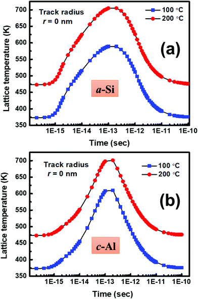 |
| | Fig. 14 Thermal spike calculation for the estimation of lattice temperature due to 100 MeV Ni ion irradiation (a) a-Si and, (b) c-Al irradiated for the track radii r = 0 nm (i.e. at the center of the track), when samples irradiated at 100 °C and 200 °C. | |
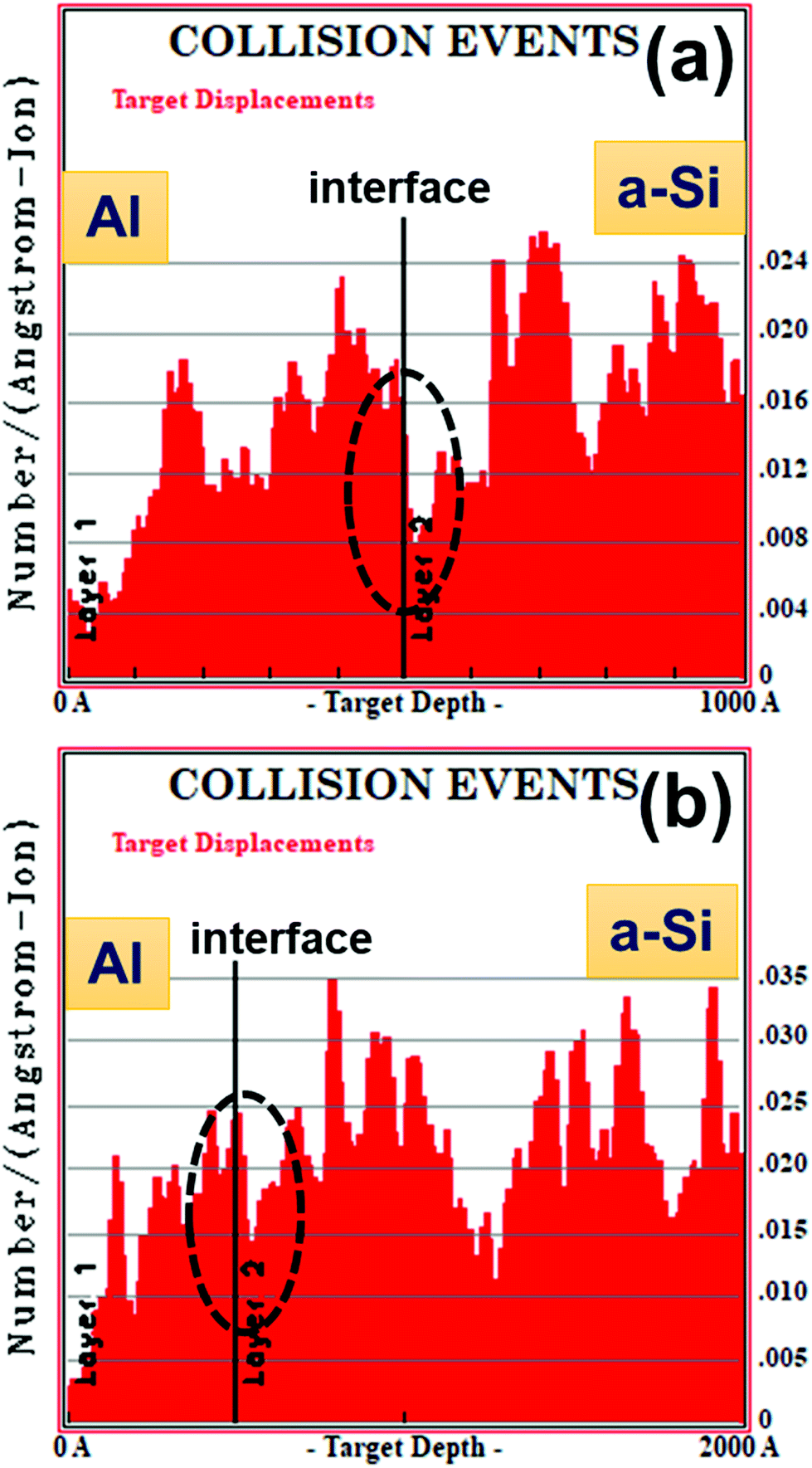
TRIM Monte-Carlo computer simulation code41 has been used to estimate the number of target displacements. Fig. 15(a) and (b) show the distribution of the number of target displacement produced due to 100 MeV Ni ion irradiation for set-A and set-B sample, respectively. The number of target displacement at the interface for set-A sample is found to be around 0.010 number/Å-ion and for set-B sample is around 0.020 number/Å-ion.
 |
| | Fig. 15 The number of target displacement/vacancies generated due 100 MeV Ni ion beam irradiation estimated using TRIM simulation code (a) for Al/a-Si thickness ratio 1:1 (i.e. set-A) samples and (b) for Al/a-Si thickness ratio 1:3 (i.e. set-B) sample. | |
It has been observed that the crystallization of Si is better in set-B sample (i.e. Al/a-Si thickness ratio 1:3) than in set-A (i.e. Al/a-Si thickness ratio 1:1) samples. This observation may be explained on the basis of larger number of atomic displacement in set-B samples than set-A samples produced near the Al/Si interface under ion irradiation as is evident from the TRIM calculations shown in Fig. 15. At some point, the interdiffusion due to stress will set in. In addition to this and as discussed before, the diffusion of Si in Al builds much more compressive stress in Al grains and tensile stress in a-Si layer. Due to these two enhanced effects, more Al tends to migrate into the underlying a-Si layer at a larger depth. Therefore, the supply of more Si atoms from the larger depth will be much higher at the interface in the case of set-B samples than in set-A samples. This would lead to faster growth of the c-Si phase in set-B samples than in set-A samples. In other words, the availability of Si atoms (i.e. concentration of Si) at the interface will be much higher in the case of set-B samples than in set-A samples, which would lead to nucleation and faster growth (i.e. crystallization) of the c-Si phase in set-B samples than in the set-A samples. The results are manifested in the higher Raman peaks in samples with thickness ratio 1:3. We also see that crystallinity is a function of temperature (see Fig. 10), which may be explained by back-diffusion of Si atoms to the matrix from the c-Si phase via vacancy mechanism. When crystallization occurs, the impurity atoms, such as Al, seem to be expelled out from the recrystallized region and accumulate at the defect sites.69 This makes recrystallized Si nearly free from Al, which has been observed at some regions near the interface, as confirmed by the XTEM image.
IV. Conclusion
In the present work, it has been shown that a-Si layer may be crystallized at lower temperature (as compared to the thermal annealing process) under irradiation using 100 MeV nickel ion beam. The effect of thickness ratio on crystallization has also been investigated. The c-Al/a-Si sample with thickness ratio of 1:3 (named as set-B) has been found to show better crystallization than the sample with thickness ratio of 1:1 (named as set-A) under ion irradiation. The crystallinity is found to decrease with increase in the ion fluence for both the set of samples. The irradiated samples at 100 °C were found to show better crystallinity than the samples at 200 °C. On the contrary, in the case of thermal annealing, the crystallization was found to start at 200 °C, and crystallinity was observed to increase with increasing temperature. Moreover, in case of thermal annealing, the c-Al/a-Si sample with thickness ratio of 1:1 (set-A) was found to show better crystallization than the sample with thickness ratio of 1:3 (set-B). The observed results have been explained in terms of defect concentration and defect dynamics under irradiation in the sample, and in particular near the interface. The results presented in this paper may have significant advantage in developing the crystalline layer at lower temperature using appropriate mask for irradiation at desired location for the future advancement in optoelectronic device application.
Conflicts of interest
There is no conflict of interest of authors.
Acknowledgements
The help received from Dr D. Kabiraj and Mr Ambuj Mishra during thermal annealing and XTEM measurement are highly acknowledged, respectively. The authors are thanks to Dr V. R. Reddy, IUC-DAE Indore for GIXRD measurement. The authors (GM & SPP) are thankful to IUAC, New Delhi for providing financial support through UFUP project (UFR-58308) to carry out this work. DK is thankful to DAE of India for the award of Raja Ramanna Fellowship. SPP is thankful to the UGC and DST, Government of India, New Delhi for supporting the Department of Pure and Applied Physics through UGC-SAP, DRS-1 and FIST Level-1 program, respectively.
References
- O. Tuzun, Y. Qiu, A. Slaoui, I. Gordon, C. Maurice, S. Venkatachalam, S. Chatterjee, G. Beaucarne and J. Poortmans, Sol. Energy Mater. Sol. Cells, 2010, 94, 1869–1874 CrossRef.
- K. R. Catchpole, M. J. McCann, K. J. Weber and A. W. Blakers, Sol. Energy Mater. Sol. Cells, 2001, 68, 173–215 CrossRef CAS.
- H. J. Park, S. Bae, S. J. Park, J. Y. Hyun, C. H. Lee, D. Choi, D. Kang, H. Han, Y. Kang, H. S. Lee and D. Kim, RSC Adv., 2019, 9, 23261–23266 RSC.
- A. S. Kale, W. Nemeth, H. L. Guthrey, S. U. Nanayakkara, V. LaSalvia, S. Theingi, D. Findley, M. Page, M. M. Al-Jassim, D. Young, P. Stradins and S. Agarwal, ACS Appl. Mater. Interfaces, 2019, 11, 42021–42031 CrossRef CAS PubMed.
- R. B. Bergmann, G. Oswald, M. Albrecht and V. Gross, Sol. Energy Mater. Sol. Cells, 1997, 46, 147–155 CrossRef CAS.
- T. Matsuyama, N. Terada, T. Baba, T. Sawada, S. Tsuge, K. Wakisaka and S. Tsuda, J. Non-Cryst. Solids, 1996, 198, 940–944 CrossRef.
- O. Nast, T. Puzzer, L. M. Koschier, A. B. Sproul and S. R. Wenham, Appl. Phys. Lett., 1998, 73, 3214–3216 CrossRef CAS.
- T. J. Konno and R. Sinclair, Philos. Mag. B, 1992, 66, 749–765 CAS.
- O. Nast and A. J. Hartmann, J. Appl. Phys., 2000, 88, 716–724 CrossRef CAS.
- O. Nast and S. R. Wenham, J. Appl. Phys., 2000, 88, 124–132 CrossRef CAS.
- Y. H. Zhao, J. Y. Wang and E. J. Mittemeijer, Appl. Phys. A: Mater. Sci. Process., 2004, 79, 681–690 CrossRef CAS.
- D. He, J. Y. Wang and E. J. Mittemeijer, J. Appl. Phys., 2005, 97, 093524–093532 CrossRef.
- D. He, J. Y. Wang and E. J. Mittemeijer, Appl. Phys. A: Mater. Sci. Process., 2005, 80, 501–509 CrossRef CAS.
- Z. M. Wang, J. Y. Wang, L. P. H. Jeurgens and E. J. Mittemeijer, Scr. Mater., 2006, 55, 987–990 CrossRef CAS.
- J. Y. Wang, D. He, Y. H. Zhao and E. J. Mittemeijer, Appl. Phys. Lett., 2006, 88, 061910–061912 CrossRef.
- J. Y. Wang, Z. M. Wang and E. J. Mittemeijer, J. Appl. Phys., 2007, 102, 113523–113531 CrossRef.
- Z. M. Wang, J. Y. Wang, L. P. H. Jeurgens and E. J. Mittemeijer, Phys. Rev. Lett., 2008, 100, 125503–125506 CrossRef CAS PubMed.
- Z. M. Wang, J. Y. Wang, L. P. H. Jeurgens and E. J. Mittemeijer, Phys. Rev. B: Condens. Matter Mater. Phys., 2008, 77, 045424–045439 CrossRef.
- Z. M. Wang, J. Y. Wang, L. P. H. Jeurgens, F. Phillipp and E. J. Mittemeijer, Acta Mater., 2008, 56, 5047–5057 CrossRef CAS.
- Z. M. Wang, L. P. H. Jeurgens, J. Y. Wang, F. Phillipp and E. J. Mittemeijer, J. Mater. Res., 2009, 24, 3294–3299 CrossRef CAS.
- Z. M. Wang, L. Gu, F. Phillipp, J. Y. Wang, L. P. H. Jeurgens and E. J. Mittemeijer, Adv. Mater., 2011, 23, 854–859 CrossRef CAS PubMed.
- Z. M. Wang, L. Gu, L. P. H. Jeurgens, F. Phillipp and E. J. Mittemeijer, Nano Lett., 2012, 12, 6126–6132 CrossRef CAS PubMed.
- S. Hu and P. C. McIntyre, J. Appl. Phys., 2012, 111, 044908–044917 CrossRef.
- T. W. Zhang, F. Ma, W. L. Zhang, D. Y. Ma, K. W. Xu and P. K. Chu, Appl. Phys. Lett., 2012, 100, 071908–071911 CrossRef.
- Y. Wei, X. Jiang, Y. Lin, X. Yang, G. Li, X. Liu, P. Lia and A. Liu, RSC Adv., 2019, 9, 6681–6688 RSC.
- T. Zhan, M. Goto, Y. Xu, Y. Kinoshita, M. Ishikiriyama and C. Nishimura, RSC Adv., 2017, 7, 7901–7905 RSC.
- O. Nast, PhD thesis, Philipps-University, Marlburg, 2000.
- O. Ebil, R. Aparicio and R. Birkmire, Thin Solid Films, 2010, 519, 178–183 CrossRef CAS.
- D. K. Avasthi and J. C. Pivin, Curr. Sci., 2010, 98, 780 CAS.
- S. P. Patel, A. K. Chawla, R. Chandra, J. Prakash, P. K. Kulriya, J. C. Pivin, D. Kanjilal and L. Kumar, Solid State Commun., 2010, 150, 1158 CrossRef CAS.
- S. P. Patel, S. A. Khan, A. K. Chawla, R. Chandra, J. C. Pivin, D. Kanjilal and L. Kumar, Phys. B, 2011, 406, 4150 CrossRef CAS.
- S. P. Patel, J. C. Pivin, M. K. Patel, J. Won, R. Chandra, D. Kanjilal and L. Kumar, J. Magn. Magn. Mater., 2012, 324, 2136 CrossRef CAS.
- T. Som, B. Satpati, P. V. Satyam, D. Kabiraj, P. Ayyub, S. Ghosh, A. Gupta, B. N. Dev and D. K. Avasthi, Nucl. Instrum. Methods Phys. Res., Sect. B, 2003, 212, 206 CrossRef CAS.
- W. Wesch, A. Kamarou and E. Wendler, Nucl. Instrum. Methods Phys. Res., Sect. B, 2004, 225, 111 CrossRef CAS.
- G. Szenes, Z. E. Horvath, B. Pecz, F. Paszti and L. Toth, Phys. Rev. B: Condens. Matter Mater. Phys., 2002, 65, 045206 CrossRef.
- T. Som, P. Ayyub, D. Kabiraj, N. Kulkarni, V. N. Kulkarni and D. K. Avasthia, J. Appl. Phys., 2003, 93, 903 CrossRef CAS.
- B. R. Chakraborty, D. Kabiraj, K. Diva, J. C. Pivin and D. K. Avasthi, Nucl. Instrum. Methods Phys. Res., Sect. B, 2006, 244, 209–212 CrossRef CAS.
- D. Bhattacharya, S. K. Srivastava, P. K. Sahoo, G. Principi, D. Kabiraj, T. Som, V. N. Kulkarni and D. K. Avasthia, Surf. Coat. Technol., 2002, 158, 59–63 CrossRef.
- D. K. Avashti, and G. K. Mehta, Swift Heavy Ions for Materials Engineering and Nanostructuring, Springer Series in Materials Science, New York, 2011, p. 145 Search PubMed.
- G. Maity, R. Singhal, S. Dubey, S. Ojha, P. K. Kulriya, S. Dhar, T. Som, D. Kanjilal and S. P. Patel, J. Non-Cryst.
Solids, 2019, 523, 119628 CrossRef CAS.
- J. F. Ziegler, J. P. Biersack and U. Littmark, The stopping and range of ions in solids, Pergamon, New York, 1985 Search PubMed.
- M. Toulemonde and C. Dufour, Phys. Rev. B: Condens. Matter Mater. Phys., 1992, 46, 362 CrossRef PubMed.
- J. B. Zeldovich, Acta Physicochim. URSS, 1943, 18, 1 Search PubMed.
- M. Avrami, J. Chem. Phys., 1940, 8, 212–224 CrossRef CAS.
- B. A Berg and S. Dubey, Phys. Rev. Lett., 2008, 100, 165702 CrossRef.
- Y. Mishima, T. Hamasaki, H. Kurata, M. Hirose and Y. Osaka, Jpn. J. Appl. Phys., 1981, 20, 121 CrossRef.
- R. Tsu, J. G. Hernandez, S. S. Chao, S. C. Lee and K. Tanaka, Appl. Phys. Lett., 1982, 40, 534–536 CrossRef CAS.
- T. Okada, T. Iwaki, H. Kasahara and K. Yamamoto, Jpn. J. Appl. Phys., 1985, 24, 161–165 CrossRef CAS.
- C. Smit, R. A. C. M. M. van Swaaij, H. Donker, A. M. H. N. Petit, W. M. M. Kessels and M. C. M. van deSanden, J. Appl. Phys., 2003, 94, 3582 CrossRef CAS.
- S. Peng, D. Hu and D. He, Appl. Surf. Sci., 2012, 258, 6003–6006 CrossRef CAS.
- M. Jiang and D. Ahn, Results Phys., 2019, 14, 102502 CrossRef.
- M. Nakamoura, Y. Kobayashi and K. Usami, Jpn. J. Appl. Phys., 1984, 23, 687 CrossRef.
- Y. Dua, Y. A. Chang, B. Huang, W. Gong, Z. Jin, H. Xu, Z. Yuan, Y. Liu, Y. He and F. Y. Xie, J. Mater. Sci. Eng. A, 2003, 363, 140–151 CrossRef.
- A. Mostafa and M. Medraj, Materials, 2017, 10, 676–724 CrossRef PubMed.
- C. F. Han, G. S. Hu, T. C. Li and J. F. Lin, Thin Solid Films, 2016, 599, 151–160 CrossRef CAS.
- Z. Wang, L. P. H. Jeurgens and E. J. Mittemeijer, Metal-Induced Crystallization-Fundamentals and Applications, Taylor & Francis Group, 2015 Search PubMed.
- K. C. Russell, J. Nucl. Mater., 1993, 206, 129–138 CrossRef CAS.
- B. Johannessen, P. Kluth, D. J. Llewellyn, G. J. Foran, D. J. Cookson and M. C. Ridgway, Appl. Phys. Lett., 2007, 90, 073119 CrossRef.
- D. J. Sprouster, R. Giulian, L. L. Araujo and P. Kluth, Phys. Rev. B: Condens. Matter Mater. Phys., 2010, 81, 155414 CrossRef.
- G. Martin, Phys. Rev. B: Condens. Matter Mater. Phys., 1984, 30, 1424 CrossRef CAS.
- D. Kanjilal, Curr. Sci., 2001, 80, 1560–1566 CAS.
- Z. G. Wang, C. Dufour, E. Paumier and M. Toulemoude, J. Phys.: Condens. Matter, 1994, 6, 6733 CrossRef CAS.
- A. Hedler, S. L. Klaumunzer and W. Wesch, Nat. Mater., 2004, 3, 804–809 CrossRef CAS PubMed.
- B. Canut, N. Bonardi, S. M. M. Ramos and S. D. Negra, Nucl. Instrum. Methods Phys. Res., Sect. B, 1998, 146, 296–301 CrossRef CAS.
- W. Wesch and E. Wendler, Ion Beam Modification of Solids: Ion-Solid Interaction and Radiation Damage, Springer Series in Surface Sciences, 2016, vol. 61 Search PubMed.
- D. Emfietzoglou, A. Akkerman and J. Barak, IEEE
Trans. Nucl. Sci., 2004, 51, 2872–2879 CAS.
- M. Kumar, P. G. Ganesan, V. N. Singh, B. R. Mehta and J. P. Singh, Nanotechnology, 2008, 19, 175606 CrossRef PubMed.
- G. J. Dienes and A. C. Damask, J. Appl. Phys., 1958, 29, 1713 CrossRef CAS.
- N. Banu, B. Satpati and B. N. Dev, Nucl. Instrum. Methods Phys. Res., Sect. B, 2017, 406, 689–696 CrossRef CAS.
|
| This journal is © The Royal Society of Chemistry 2020 |
Click here to see how this site uses Cookies. View our privacy policy here. 
 Open Access Article
 This Open Access Article is licensed under a Creative Commons Attribution-Non Commercial 3.0 Unported Licence
 e,
S. Dharf,
T. Somg,
D. Kanjilale and
Shiv P. Patel
e,
S. Dharf,
T. Somg,
D. Kanjilale and
Shiv P. Patel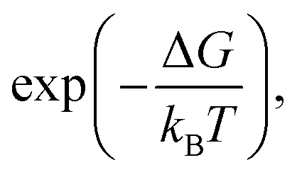 where ΔG is the free energy enthalpy for forming the surface of the expanding nucleus and the difference in bulk energy between the forming phase and the earlier phase. The formation of the c-Si phase is thermodynamically favorable as this process results in reduction of the overall free energy of the bilayer system. The subsequent growth of the c-Si nucleus occurs due to the arrival of more and more Si atoms to the c-Si nuclei. The growth of the c-Si phase is governed by Kolmogorov–Johnson–Mehl–Avrami (KJMA) theory,44,45 which relates the fraction of transformed crystalline phase (ftrans) to the annealing time (t):
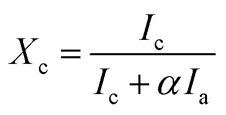 where, α is the ratio of the integrated Raman cross-section for c-Si to a-Si, known as optical absorption correction factor,
 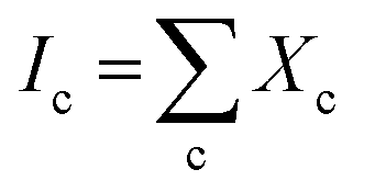 and
and  and Σ is the integrated cross-section over the resolved frequency range. To calculate Xc, the value of α has been taken as 0.8 from the literatures.47,50,51 This value of α is reasonable because the optical properties of the crystalline and amorphous phases are similar in a film coexistent with μc-Si and a-Si.48 Very recently, Jiang et al.51 used this method to determine Xc of Ge in Al-induced crystalline Ge system. Fig. 2 shows the calculated crystalline volume fraction of set-A and set-B samples annealed at different temperatures. The Xc values are found to be zero for the pristine sample and the sample annealed at 100 °C in both set of samples, which shows the absence of crystallization in the samples. The Xc value is found to be 90.22% when the samples are annealed at 200 °C; increasing the annealing temperatures further results in the increase in Xc value, which goes to 92.86% at 500 °C, for set-A samples. Similarly, the Xc value is found to be 89.12% when the samples are annealed at 200 °C; increasing the annealing temperatures further results in the increase in Xc value, which goes to 91.12% at 500 °C, for set-B samples.