
 Open Access Article
 This Open Access Article is licensed under a Creative Commons Attribution-Non Commercial 3.0 Unported Licence
Bottom-up fabrication of the multi-layer carbon metal nanosheets
H. Hamoudi*a,
G. R. Berdiyorov a,
K. Arigab and
V. Esaulovc
a,
K. Arigab and
V. Esaulovc
aQatar Environment and Energy Research Institute, Hamad Bin Khalifa University, Doha, Qatar. E-mail: hhamoudi@hbku.edu.qa; hichamhamoudia@gmail.com
bNational Institute of Material Science NIMS, Tsukuba, Japan
cInstitut des Sciences Moléculaires d'Orsay, UMR 8214 CNRS-Université, bât 520, Université Paris Sud, Université Paris Saclay, Orsay 91405, France
First published on 24th February 2020
Abstract
Ordered carbon composite materials have great potential for practical applications in many areas such as energy conversion, quantum computing, biotechnologies, and electronics. In this work, we demonstrate a state-of-the-art self-assembly driven building block approach to create new layered carbon–metal composite materials with advanced properties. We fabricate molecular nanocomposites using self-assembled metal intercalated multi-layers of dithiol derivatives. The obtained structures are analysed using different characterization tools (such as X-ray photoelectron and Raman spectroscopy and atomic force microscopy) and their electronic transport properties are studied by four-point probe measurements supplemented by density functional theory calculations. This work demonstrates a new strategy for low-cost, high-yield and eco-friendly nanofabrication of hybrid organometallic membranes.
Introduction
Self-assembly or spontaneous formation of matter is the principal mechanism responsible for the creation of the most complex structures in nature. It has been shown that self-assembled monolayers (SAMs) can be used to form thick, highly ordered molecular carbon systems.1–3 Going beyond the self-assembled monolayers, conjugate organic molecules can lead to new hybrid materials with novel functionalities, which can open new vistas in nanoelectronics and nanotechnology.4–8 A particular focus has been to create new functional materials for information processing and energy conversion using the self-assembly strategy. For example, Wytko et al.,7 have presented two self-assembly approaches for porphyrin derivatives that have potential for future nanotechnology development. Hamoudi5 has shown the possibility of creating carbon nanomembranes after modification of conjugate SAMs by electron beams and/or UV light. Such an irradiation leads to the formation of a cross-linked molecular network in the aromatic systems by the cleavage of the C–H bonds. The cross-linked systems can be detached from the substrate yielding a molecular monolayer thick carbon nanomembrane.1 Such functional nanosheets can be used for different applications such as molecular electronics and catalysis.4,6,9–14Creation and properties of carbon nanomembranes by lateral cross-linking of aromatic molecular SAMs by electron irradiation have been studied in the past by several research groups (see ref. 1, 2, 15 and 16 for reviews). For example, Chesneau et al.17 studied the effect of low-energy electron beams on aromatic fluorocarbon SAMs on metallic substrates using different characterization tools. A clear dominance of molecular cross-linking over molecular decomposition was reported. Similar results were reported by Geyer et al. for 1,1′-biphenyl-4-thiol SAMs.18 Detailed analysis of the mechanisms of such electron-irradiation-induced cross-linking in aromatic SAMs was presented in ref. 19 and 20. The resulting cross-linked aromatic SAMs can be isolated from the substrate and their properties can further be tuned by surface functionalization.21 Further heat treatment will transform these mechanically stable carbon nanomembranes into functionalized graphene sheets.22–24 These studies show the great potential of self-assembly and consequent cross-linking processes for creating molecular-thick nanomembranes/nanosheets with pronounced mechanical, thermal and chemical stabilities.
In this work we demonstrate the possibility of creating multilayer molecular nanocomposites (nanomembranes) starting from self-assembled molecular monolayers. We use the self-assembly of nickel (Ni) atom intercalated 5,5′-bis(mercaptomethyl)-2,2′-bipyridine (BPD, HS-CH2-(C5H3N)2-CH2-SH) and 1,4-benzenedimethanethiol (BDMT, HS-CH2-(C6H4)-CH2-SH) dithiol (DT) multilayers on gold substrate. To obtain multilayers of such dithiol-end molecular SAMs, we follow the approach presented in ref. 25 and 26. Namely, we start by exposing the DT monolayer to a concentrated Ni ion solution, which results in grafting of Ni atoms on the sulfur-end group as has been described for Cu atom grafting.27 The resulting DT–Ni SAM are then immersed in a DT solution to obtain a DT–Ni–DT bilayer. Repetition of this process results in the formation of ordered multilayer structures. Using electron beam irradiation, we convert the resulting multilayer of molecular SAMs into a multilayered carbon–metal nanomembrane.5 The resulting film is characterized by various complementary techniques such as X-ray photoelectron, atomic force microscopy, and electrical four-point probe measurements. These nanomembranes represent a new type of functional two-dimensional (2D) materials, which can also be concisely described as surfaces without bulk.15 Similar to single layer self-assembly-based nanomembranes2,15 or layer-by-layer nanomembranes,28 the proposed multilayer nanomembranes have a potential for diverse applications. For example, these nanostructures can be used for materials separation and filtration because of their low dimensional nature, elasticity, enhanced mechanical and thermal properties. Tuneable conductivity due to predefined layer sequence and surface functionalization makes these materials strong candidates for nanoelectronics and optoelectronics, such as ultrasensitive sensors and biodetectors. In the following sections we give a detailed description for the fabrication and characterization of these multilayer metal organic heterostructures and the formation of carbon nanosheets from them after annealing.
Experimental
The gold support for SAM fabrication was prepared by thermal evaporation of 150 nm of gold (99.99% purity) onto either polished single-crystal silicon (100) wafers coated with a 10 nm titanium layer or on freshly cleaved and degassed mica with deposition performed at about 350 °C. After that the SAM of the 5,5′-bismercaptomethyl-2,2′-bipyridine (BPD) (see Fig. 1) was prepared by immersion of the gold support into a freshly prepared 1 mM solution of n-hexane for 30 min at 60 °C.29,30 As in our previous studies,1 we used solutions well-degassed by Ar and all preparation steps were performed in the absence of ambient light. After the gold wafer was modified with a layer of BPD, the system was held for 3 h in contact with a concentrated aqueous solution of NiCl2. The resulting BPD–Ni SAM was then incubated in the BPD solution as in the 1st step to yield the BPD–Ni–BPD bilayer. Finally, this bilayer was held for 3 h in contact with a concentrated aqueous solution of NiCl2 to yield a Ni terminated BPD–Ni–BPD–Ni layer. This procedure was continued to form BPD–Ni multilayer films.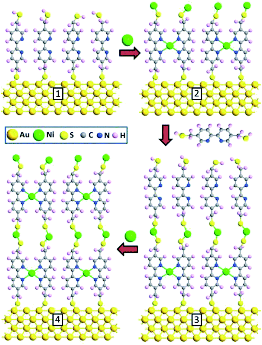 | ||
| Fig. 1 Schematics of the sequential reactions to prepare BPD–Ni–BPD–Ni multilayer. | ||
The multi-layer films fabricated as described above were characterized by X-ray photoelectron spectroscopy (XPS). XPS spectroscopy measurements were conducted at the MANA Foundry using the XPS Thermo Fisher (Alpha 110 mm analyser: Sigma XPS version). The XPS spectra were recorded in the C 1s, N 1s, S 2p, and Ni 2p regions. The spectra acquisition was performed in normal emission geometry using the Al K radiation. The binding energy (BE) scale of each spectrum was individually calibrated to the Au 4f7/2 emission of an n-alkanethiol covered gold substrate at 83.95 eV.
The multi-layer stacked SAMs were exposed to electron irradiation using an e-beam lithography system Elionix Inc (50 kV, 60 mC cm−2) to form carbon–metal nanosheets (CMNS).1,31 This leads to intralayer cross linking of the SAM multilayer. The CMNS was released as described in a previous work.1 A PMMA film was spin-coated onto a 1 cm2 of the crosslinked SAM and baked at 180 °C for 3 min on a hot plate. The gold film was cleaved from the mica in hydrofluoric acid solution and etched away in an I2/KI bath. In the next step, the nanomembrane/PMMA was transferred onto a SiO2 substrate followed by dissolution of the PMMA in acetone to release a CMNS. The resulting nanomembranes are then ready to be transferred to an appropriate substrate for further analysis.
The morphology of the resulting membranes was investigated using a Hitachi S-4300 scanning electron microscope equipped with a W tip cold-FE electron emitter. The AFM topographical and thickness data were collected using a Veeco Multimode SPM microscope in the tapping mode. The mono and the multilayers were electrically tested on a multiprobe station using a semiconductor parameter analyzer (Keithley Instruments Inc.) at room temperature and under vacuum to avoid the influence of water.
Results and discussion
We start with building molecular nanocomposites using highly ordered and closely packed self-assembled multi-layers of bipyridine derivatives such as BPD (5,5′-bis(mercaptomethyl)-2,2′-bipyridine)–Ni2+ as schematically presented in Fig. 1. The BPD SAM has two active centres for metal ions: (i) the bipyridine group which is a well-characterized metal acceptor is utilized for various supramolecular assemblies4 and (ii) the pending S–H end group which allows grafting of metallic ions in case of a standing up SAM. This reactivity between the molecules and metal ions makes the implementation of the lateral and the vertical assembly architecture possible. The sequential immersion of the Au substrate into the BPD solution and Ni2+ engenders a SAM based multilayer (as depicted in Fig. 1) and enables one to control the thickness of the resulting nanomembranes. Note that the present method of creating multi-layered nanomembranes is conceptually different than the layer-by-layer technique for creating ultrathin polymeric membranes.28,32 In the latter case different positively and negatively charged polyelectrolytes are usually used, which increases the cost of nanofabrication.We start by studying the effect of cross-linking on the properties of SAMs. As a reference, we studied the effect of electron irradiation on the structural properties of aliphatic C12 SAMs. Fig. 2(a) and (b) show the XPS spectra of such molecules before (black curves) and after (red curves) electron irradiation. It is seen from Fig. 2(a) that the intensity of C 1s signal reduces by almost 50% after electron bombardment, indicating the instability of this SAM. Similar degradation is also obtained for S 2p spectra. The reduction of the carbon content indicates significant damage upon irradiation, resulting in desorption of the aliphatic molecules without lateral cross-linking as illustrated in Fig. 2(d). The dominant process is expected to be the decomposition of the alkyl chains and capture of the released alkylsulfide moieties in the aliphatic matrix.34,35
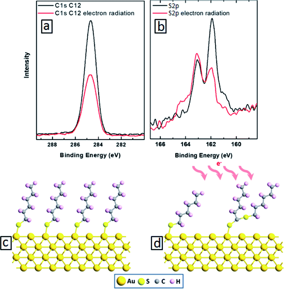 | ||
| Fig. 2 C 1s (a) and S 2p (b) XPS spectra of the self-assembled C12 molecules before (black curves) and after (red curves) electron irradiation. (c and d) Schematics C12 SAM before (c) and after (d) electron bombardment. | ||
To study the effect of electron irradiation on the morphological stability of our aromatic molecules, we have conducted XPS analysis of BPD–Ni SAMs before and after electron irradiation. Fig. 3(a) and (b) show C 1s (a) and S 2p (b) XPS spectra before (black curves) and after (red curves) electron beam impact. We obtained only small (∼5%) reduction of C 1s signal after irradiation (Fig. 3(a)), indicating efficient cross-linking without damage to the SAM morphology. For the given dose of the irradiation, the amplitude of the maximum of S 2p signal remains unchanged (Fig. 3(b)). Small local maximum appear near 168 eV, which can be related to the formation of sulfite bonds during the irradiation. These results indicate the stability of BPD SAMs against electron bombardment. Fig. 3(e) illustrates the ideal case of intermolecular cross-linking of BPD–Ni SAMs after electron irradiation. However, depending on the level of electron irradiation as well as packing structure of the molecules, a variety of partially cross-linked structures can be obtained as revealed in quantum chemical calculations.36 Cross-linking has also a positive effect on the mechanical, thermal, chemical and electronic properties of SAMs. For example, Turchanin et al. have shown that the cross-linked SAMs of aromatic molecules can exhibit thermal stability up to 1000 K.37 Enhanced mechanical properties of cross-linked SAMs were reported in ref. 24. The cross-linked SAMs have also shown exceptional chemical stability.18,38,39
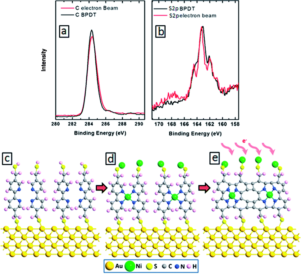 | ||
| Fig. 3 C 1s (a) and S 2p (b) XPS spectra of the self-assembled BPD molecules before (black curves) and after (red curves) electron irradiation. (c–e) Schematics of BPD SAM before (c and d) and after (e) electron bombardment. | ||
In what follows, we will present the results only for cross-linked multi-layered structures. Fig. 4(a) shows the C 1s XPS spectra of the BPD–Ni–BPD–Ni film. The XPS of the monolayer have been reported in a previous work.1 The main peak at 285.5 eV is a superposition of the contribution from different carbon atoms: the aliphatic moieties (CH2) and the meta, para C in the pyridine unit, and the ortho C in the rings directly bonded to the nitrogen atoms.1 In the case of N 1s spectra (Fig. 4(b)), a chemical shift of the main peak towards high binding energy is observed, because of the binding of the bipyridine sites to the Ni2+ moiety as noted in pervious works.1,27 Some spectra are decomposed into the individual contribution related to the different species (see the corresponding text for details).
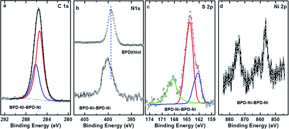 | ||
| Fig. 4 C 1s (a), N 1s (b), S 2p (c), and Ni 2p (d) XPS spectra of the multilayer SAM of the BPD on gold substrate. In the case of nitrogen, the N 1s spectrum is compared to that for the BPD SAM. | ||
The spectral deconvolution of the S 2p spectra of the BPD–Ni–BPD–Ni SAM (see Fig. 4(c)) shows three doublets. The S 2p3/2 component of the first one lies at 162 ± 1 eV (S1), and that of the second doublet at 163.5 ± 2 eV (S2). The highest lying peak at about 168 eV is due to some oxidation, presumably related to immersion in water. For the BPD SAM the S1 component corresponds to thiolate sulfur bound to the substrate and the S2 component to the free SH at the outer surface of the BPD SAM. We observed changes in relative intensities of the S1 and S2 components due to Ni binding to the outer SH group.1 Thus, upon first immersion into the Ni solution, the S2 component intensity decreases due to Ni binding to the outer SH group.4 This leads to a change in the S 2p binding energy which becomes similar to that of the thiolate S bound to the Au substrate.4,15 Thereafter the S2 intensity again increases due to binding on BPD and appearance of free SH on the outer BPD layer. The final BPD–Ni–BPD–Ni layer spectrum reveals a continuing existence of some S2 component, indicating that the Ni coverage was not complete for the immersion time used.15 The increase in both S1 and S2 doublets after re-immersion into the BPD solution confirms the formation of the bilayer as was studied before.15 The thickness of the BPD–Ni–BPD–Ni film determined by XPS is ∼5.4 nm, showing a good agreement with the formation of bilayers of BPD.1,15
XPS was also used to study the chemical composition of the freestanding nanomembranes, prepared after the electron irradiation as described above. The resulting carbon membranes after electron-irradiation-induced polymerization were detached from the metallic substrate by chemical etching of the metal after polymer spin-coating.24 Fig. 5 shows the C 1s, N 1s, S 2p, and Ni 2p spectra of the nanomembranes transferred to SiO2 substrates. The S 2p XPS spectra of the BPD–Ni–BPD–Ni nanomembranes are shown in Fig. 5(c). The spectra of the BPD–Ni–BPD–Ni nanomembrane exhibit two distinct features. The main broad and distinctly asymmetric peak at ∼163.8 eV for the BPD–Ni–BPD–Ni systems, is a superposition of the contributions from the Ni–thiolate species, free thiol groups and possibly disulfide (S–S) linkages, while the second, relatively weaker emission located at ∼168.00 eV is associated with the sulfur atom bonded to oxygen. There are no remarkable changes in the N 1s, C 1s, and Ni 2p XPS spectra compared to the BPD–Ni reported previously1 and BPD–Ni–BPD–Ni films before and after the irradiation.
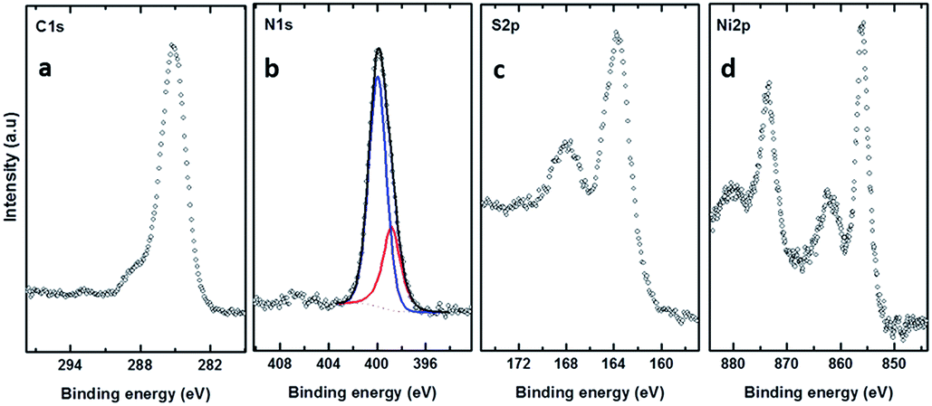 | ||
| Fig. 5 C 1s, N 1s, S 2p, and Ni 2p XPS spectra of the free standing membrane of BPD–Ni–BPD–Ni. The N 1s spectra have been decomposed into the individual contribution related to the different species; see the text for details. | ||
The thickness of the nanosheets determined by AFM (see Fig. 6(a)–(c)) are ∼3 nm for the BPD–Ni and ∼6 to 8 nm for the BPD–Ni–BPD–Ni nanomembranes, which is in reasonable agreement with the thickness obtained using XPS for the related SAMs. The 3D AFM images of the freestanding nanosheets show 2D triangles morphology (see Fig. 7(a) and (b)). This is probably due to the replication of the surface morphology of the gold (111) terraces on mica.33 Namely, this morphology is a consequence of localization of the cross-linked areas in the Au (111) terraces, where the highest molecular packing densities are formed.
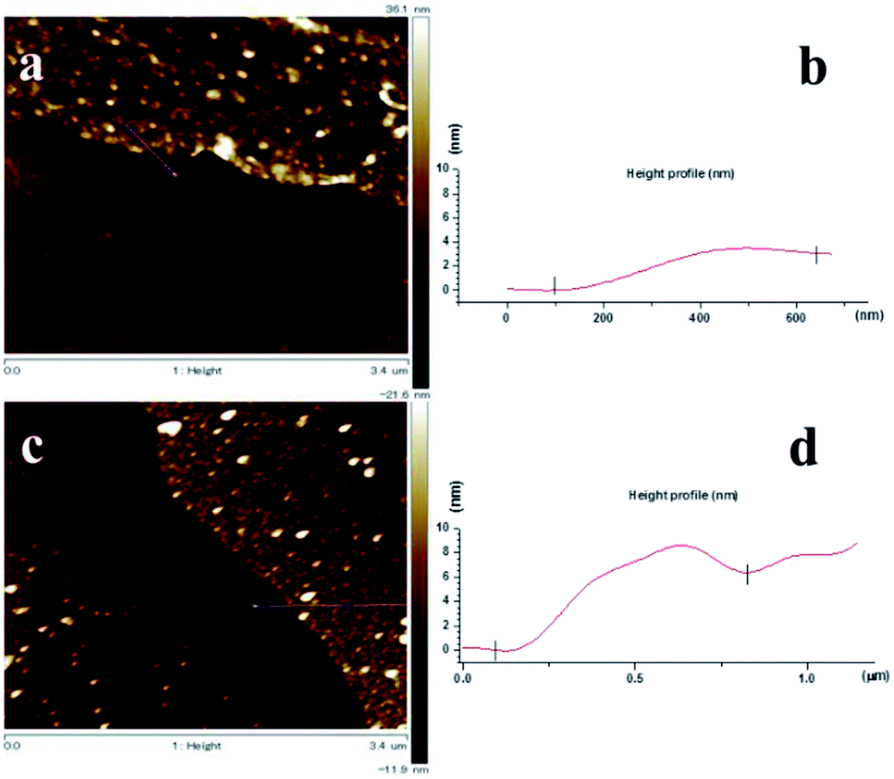 | ||
| Fig. 6 AFM images of the BPD–Ni and BPD–Ni–BPD–Ni nanomembranes on Si. The nanomembranes are prepared by electron radiation of the structure 2 and 4 (see Fig. 1) and then detached by dissolving the gold substrate: (a) AFM image of the BPD–Ni nanomembrane on Si, (b) AFM height profile of the BPD–Ni nanomembrane on Si, (c) AFM image of the BPD–Ni–BPD–Ni nanomembrane, (d) AFM height profile of the BPD–Ni–BPD–Ni nanomembrane. | ||
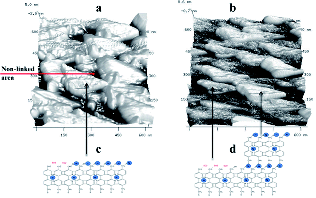 | ||
| Fig. 7 3D AFM images of the nanomembranes using taping mode: BPD–Ni nanosheet, (b) BPD–Ni–BPD–Ni nanosheet, (c and d) cartoons of The BPD–Ni, and BPD–Ni–BPD–Ni nanosheets. | ||
A proposed architecture of the organometallic membranes is presented in Fig. 7(c) and (d). Electron irradiation of the SAMs produces carbon–carbon links between neighbouring molecules,3 which reduce the spatial separation between molecules. The black, lower height areas in the 3D AFM images (Fig. 7(a) and (b)) are presumably due to regions with non-linked molecules. These images also show the differences in the architectures between the mono- and multi-layer freestanding nanosheets. The BPD–Ni–BPD–Ni sheets have areas of lower thickness due to presence of remaining BPD–Ni sheet. Partial contamination of the free S–H group of the first monolayer by O2 (see Fig. 1 panel 1), becomes a barrier to the formation of a well-packed second layer. The BPD–Ni system shows a lower concentration of the non-linked areas (black areas) compared to the BPD–Ni–BPD–Ni configuration.
In order to obtain graphene-like layered membranes, the BPD–Ni–BPD–Ni nanosheet was annealed under N2 atmosphere at temperatures up to 600 °C for 20 min. Fig. 8(a) shows a Raman spectrum of the annealed BPD–Ni–BPD–Ni nanosheet compared to the annealed BPD–Ni nanosheet on SiO2 (measured using an excitation wavelength of 532 nm). In both cases the graphitization was confirmed by the presence of the D (1365 cm−1) and G (1587 cm−1) peaks. Similar Raman spectra were reported on different carbon nanomembranes.2,5 The D band is associated with the presence of defects in the carbon matrix. In addition, the BPD–Ni–BPD–Ni system shows splitting of the G peak into doublet structures G1 and G2: a finger print of graphite intercalation compounds (GICs). A downward shift of G2 was observed for the n-doped multilayer graphene film. Increasing the number of sheets in a stack of the annealed BPD–Ni–BPD–Ni film causes an increase in G2 band intensities see Fig. 8.
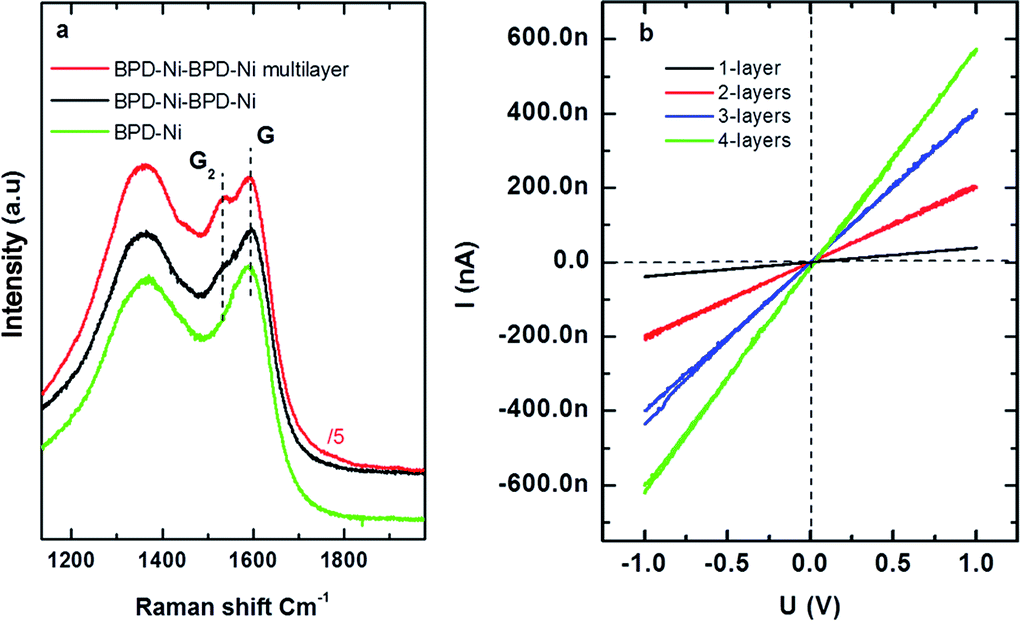 | ||
| Fig. 8 Raman shift and four probes IV characteristics of the annealed nanosheet. (a) Raman shift of the annealed BPD–Ni–BPD–Ni nanosheet, and (b) room temperature for probes' current versus voltage of the annealed BPD–Ni–BPD–Ni nanosheet. Each curve corresponds to 1, 2, 3, and 4 layers of annealed BPD–Ni–BPD–Ni system. | ||
The electrical properties of the annealed BPD–Ni–BPD–Ni system were investigated as a function of the number of layers in a stack. Fig. 8(b) shows I–V characteristics obtained using four probe measurements. The I–V curve of the single and the multi layers in the stack system remains linear, showing metallic behaviour. The conductivity increases with the increase of the number of sheets, which shows good agreement with a previous study of the similar system prepared in a water hexane interface.6
To model the effect of metal atom inclusions between the graphitic layers on the electronic structure of the annealed film, we consider a simplified model with idealized graphene multilayers with Ni atom inclusions (see Fig. 9). Each graphene layer contains 18 C atoms and a single Ni atom is placed between the layers. We have considered systems with up to 8 graphene layers (Fig. 9(d)). The structural optimization and electronic structure calculations are conducted using density functional theory (DFT) within the generalized gradient approximation of Perdew–Burke–Ernzerhof (PBE)36 for the exchange-correlation energy. Non-bonded van der Waals interactions are taken into account using Grimme's PBE-D3 empirical dispersion correction.40 The Brillouin zone integration was conducted using 6 × 6 × 6 k-points sampling.41 During the geometry optimization, both atomic positions and lattice parameters are relaxed using the convergence criterion for Hellman–Feynman forces as 0.01 eV Å−1. All the calculations are conducted using the Vienna ab initio simulation package VASP.42,43
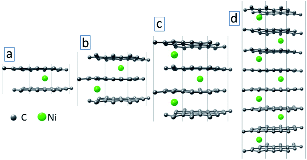 | ||
| Fig. 9 Optimized structures of graphene multilayers (L = 2 (a), 3 (b), 4 (c) and 8 (d)) with Ni atom intercalations. | ||
Fig. 10(a) shows the total density of states (DOS) of the systems with 2, 3, 4 and 8 graphene layers (see Fig. 9 for the optimized structures). Starting from bilayer graphene (black curve in Fig. 10(a)), the metal intercalation results in metallic behaviour of the system (i.e., non-zero DOS near the Fermi level). With the increase of the number of graphene layers, the region with reduced DOS near the Fermi level becomes smaller (see red and green curves in Fig. 10(a)). Enhanced DOS and reduced “gap” became still more pronounced for the system with 8 graphene layers (see blue curve in Fig. 10(a)). This will increase the charge carrier transport across the system as was obtained in the experiment (see Fig. 6(b) for the I–V curves). Fig. 10(b) and (c) show the DOS of the considered systems projected on C and Ni atoms. It is seen from these figures that C atoms contribute more to the DOS of the system in the conduction band. The contribution of the Ni atoms is obtained mostly in the valence band. In both cases, peaks in the DOS disappear with increase of the number of graphene layers, except larger peaks away from the Fermi level.
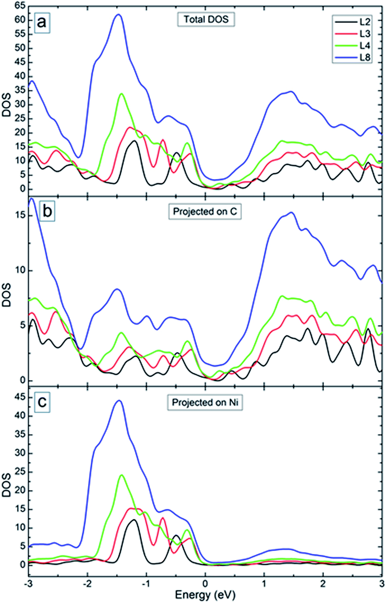 | ||
| Fig. 10 (a) Total density of states of the considered systems. (b and c) Partial density of states of C (b) and Ni (c) atoms. The energy origin is set at the Fermi energy. | ||
Conclusions
Using self-assembly of bipyridine derived molecules we fabricated a multi-layered metal intercalated superlattice structure. In addition, the created structures are subjected to electron irradiation to enhance their mechanical and chemical stability. The system was further transformed into a graphitic carbon–metal nanocomposite by annealing. The characterization of the resulting structures using X-ray photoelectron spectroscopy, atomic force microscopy and Raman spectroscopy, revealed the formation of a stable architecture of the organometallic nanocomposite. The effect of metal atom inclusions on the electronic structure and charge transport properties are studied using electrical measurements. Enhanced charge carrier transport is obtained in our multilayer carbon structures due to metal ion intercalation. The experimental results are supplemented by DFT computer simulations, which demonstrate changes in the electronic structure of the materials leading to the experimentally obtained changes in transport properties. These findings will be useful in creating functional hybrid organometallic structures with enhanced stability.Conflicts of interest
There are no conflicts to declare.Acknowledgements
Computational resources were provided by the research computing center at Texas A&M University in Qatar.Notes and references
- H. Hamoudi, RSC Adv., 2014, 4, 22035–22041 RSC.
- A. Turchanin and A. Gölzhäuser, Adv. Mater., 2016, 28, 6075–6103 CrossRef CAS PubMed.
- X. Zhang, M. Mainka, F. Paneff, H. Hachmeister, A. Beyer, A. Gölzhäuser and T. Huser, Langmuir, 2018, 34, 2692–2698 CrossRef CAS PubMed.
- H. Hamoudi and V. A. Esaulov, Ann. Phys., 2016, 528, 242–263 CrossRef CAS.
- H. Hamoudi, J. Mater. Chem. C, 2015, 3, 3636–3644 RSC.
- H. Fan and W. Shen, ChemSusChem, 2015, 8, 2004–2027 CrossRef CAS PubMed.
- J. A. Wytko, R. Ruppert, C. Jeandon and J. Weiss, Chem. Commun., 2018, 54, 1550–1558 RSC.
- M. Gobbi, E. Orgiu and P. Samorì, Adv. Mater., 2018, 30, 1706103 CrossRef PubMed.
- K. Ariga, M. Nishikawa, T. Mori, J. Takeya, L. K. Shrestha and J. P. Hill, Sci. Technol. Adv. Mater., 2019, 20, 51–95 CrossRef CAS.
- K. Ariga, M. Ito, T. Mori, S. Watanabe and J. Takeya, Nano Today, 2019, 100762 CrossRef.
- K. Ariga, M. Matsumoto, T. Mori and L. K. Shrestha, Beilstein J. Nanotechnol., 2019, 10, 1559–1587 CrossRef CAS PubMed.
- K. Ariga, E. Ahn, M. Park and B. S. Kim, Chem.–Asian J., 2019, 14, 2553–2566 CrossRef CAS PubMed.
- K. Ariga, X. Jia and L. K. Shrestha, Mol. Syst. Des. Eng., 2019, 4, 49–64 RSC.
- K. Ariga, T. Mori and L. K. Shrestha, Chem. Rec., 2018, 18, 676–695 CrossRef CAS PubMed.
- A. Turchanin and A. Gölzhäuser, Prog. Surf. Sci., 2012, 87, 108–162 CrossRef CAS.
- P. Angelova and A. Gölzhäuser, Phys. Sci. Rev., 2017, 2, 1–19 CrossRef.
- F. Chesneau, H. Hamoudi, B. Schüpbach, A. Terfort and M. Zharnikov, J. Phys. Chem. C, 2011, 115, 4773–4782 CrossRef CAS.
- W. Geyer, V. Stadler, W. Eck, M. Zharnikov, A. Gölzhäuser and M. Grunze, Appl. Phys. Lett., 1999, 75, 2401 CrossRef CAS.
- A. Turchanin, D. Käfer, M. El-Desawy, C. Wöll, G. Witte and A. Gölzhäuser, Langmuir, 2009, 25, 7342–7352 CrossRef CAS PubMed.
- L. Amiaud, J. Houplin, M. Bourdier, V. Humblot, R. Azria, C. M. Pradier and A. Lafosse, Phys. Chem. Chem. Phys., 2014, 16, 1050–1059 RSC.
- W. Eck, A. Küller, M. Grunze, B. Völkel and A. Gölzhäuser, Adv. Mater., 2005, 17, 2583–2587 CrossRef CAS.
- P. Angelova, H. Vieker, N.-E. Weber, D. Matei, O. Reimer, I. Meier, S. Kurasch, J. Biskupek, D. Lorbach, K. Wunderlich, L. Chen, A. Terfort, M. Klapper, K. Müllen, U. Kaiser, A. Gölzhäuser and A. Turchanin, ACS Nano, 2013, 7, 6489–6497 CrossRef CAS PubMed.
- D. G. Matei, N.-E. Weber, S. Kurasch, S. Wundrack, M. Woszczyna, M. Grothe, T. Weimann, F. Ahlers, R. Stosch, U. Kaiser and A. Turchanin, Adv. Mater., 2013, 25, 4146–4151 CrossRef CAS PubMed.
- A. Turchanin, A. Beyer, C. T. Nottbohm, X. Zhang, R. Stosch, A. Sologubenko, J. Mayer, P. Hinze, T. Weimann and A. Gölzhäuser, Adv. Mater., 2009, 21, 1233–1237 CrossRef CAS.
- H. Hamoudi, K. Uosaki, K. Ariga and V. A. Esaulov, RSC Adv., 2014, 4, 39657–39666 RSC.
- Y. Tong, T. Jiang, S. Qiu, K. Koshmak, A. Giglia, S. Kubsky, A. Bendounan, L. Chen, L. Pasquali, V. A. Esaulov and H. Hamoudi, J. Phys. Chem. C, 2018, 122, 2880–2889 CrossRef CAS.
- M. Brust, P. M. Blass and A. J. Bard, Langmuir, 1997, 13, 5602–5607 CrossRef CAS.
- G. Decher, Science, 1997, 277, 1232–1237 CrossRef CAS.
- H. Hamoudi, M. Prato, C. Dablemont, O. Cavalleri, M. Canepa and V. A. Esaulov, Langmuir, 2010, 26, 7242–7247 CrossRef CAS PubMed.
- H. Hamoudi, Z. Guo, M. Prato, C. Dablemont, W. Q. Zheng and B. Bourguignon, Phys. Chem. Chem. Phys., 2008, 10, 6836–6841 RSC.
- H. Hamoudi, Nanoscale Res. Lett., 2014, 9, 287 CrossRef PubMed.
- Y. Lvov, G. Decher and H. Möhwald, Langmuir, 1993, 9, 481–486 CrossRef CAS.
- S. Buchholz, H. Fuchs and J. P. Rabe, J. Vac. Sci. Technol., B: Microelectron. Nanometer Struct.--Process., Meas., Phenom., 1991, 9, 857–861 CrossRef CAS.
- H. Hamoudi, F. Chesneau, C. Patze and M. Zharnikov, J. Phys. Chem. C, 2011, 115, 534–541 CrossRef CAS.
- A. Gölzhäuser, W. Geyer, V. Stadler, W. Eck, M. Grunze and K. Edinger, J. Vac. Sci. Technol., B: Microelectron. Nanometer Struct.--Process., Meas., Phenom., 2000, 18, 3414–3418 CrossRef.
- J. P. Perdew, K. Burke and M. Ernzerhof, Phys. Rev. Lett., 1996, 77, 3865 CrossRef CAS PubMed.
- A. Turchanin, M. El-Desawy and A. Gölzhäuser, Appl. Phys. Lett., 2007, 90, 053102 CrossRef.
- A. Turchanin, A. Tinazli, M. El-Desawy, H. Großmann, M. Schnietz, H. H. Solak, R. Tampé and A. Gölzhäuser, Adv. Mater., 2008, 20, 471–477 CrossRef CAS.
- A. Turchanin, M. Schnietz, M. El-Desawy, H. H. Solak, C. David and A. Gölzhäuser, Small, 2007, 3, 2114–2119 CrossRef CAS PubMed.
- S. Grimme, J. Comput. Chem., 2006, 27, 1787 CrossRef CAS PubMed.
- H. J. Monkhorst and J. D. Pack, Phys. Rev. B: Condens. Matter Mater. Phys., 1976, 13, 5188 CrossRef.
- G. Kresse and J. Furthmuller, Comput. Mater. Sci., 1996, 6, 15 CrossRef CAS.
- G. Kresse and D. Joubert, Phys. Rev. B: Condens. Matter Mater. Phys., 1999, 59, 1758 CrossRef CAS.
| This journal is © The Royal Society of Chemistry 2020 |