
 Open Access Article
 This Open Access Article is licensed under a Creative Commons Attribution-Non Commercial 3.0 Unported Licence
Atomic scale study of black phosphorus degradation†
Changbae Hyun *a,
Jong Hun Kimb,
Jong-Young Leec,
Gwan-Hyoung Lee*bde and
Kwang S. Kim*f
*a,
Jong Hun Kimb,
Jong-Young Leec,
Gwan-Hyoung Lee*bde and
Kwang S. Kim*f
aDepartment of Physics, Pohang University of Science and Technology, Pohang 37673, Republic of Korea. E-mail: cbhyun@postech.ac.kr
bDepartment of Materials Science and Engineering, Seoul National University, Seoul, 08826, Republic of Korea. E-mail: gwanlee@snu.ac.kr
cDepartment of Materials Science and Engineering, Yonsei University, Seoul, 03772, Republic of Korea
dResearch Institute of Advanced Materials (RIAM), Seoul National University, Seoul, 08826, Republic of Korea
eInstitute of Applied Physics, Seoul National University, 08826, Republic of Korea
fCenter for Superfunctional Materials, Department of Chemistry, Ulsan National Institute of Science and Technology (UNIST), Ulsan 44919, Republic of Korea. E-mail: kimks@unist.ac.kr
First published on 2nd January 2020
Abstract
Black phosphorus (BP) is a promising two-dimensional (2D) material for future electronic devices due to its unique properties of high carrier mobility and large band gap tunability. However, thinner crystalline BP is more readily degraded under ambient conditions. For BP-based electronic devices, degradation of the exfoliated BP is a key issue. However, the nanometer scale study of BP degradation is rare so far. Herein, we report an atomically resolved degradation process of the BP surface using atomic force microscopy under temperature- and humidity-controlled environments. The atomically resolved crystal surface of BP deteriorated due to surface etching after cleavage, and showed monolayer etching. The etching process is accelerated by applying a bias voltage to BP via a conductive tip. After the voltage-assisted BP etching, the BP etching product shows crystalline BP confirmed by Raman spectroscopy and atomic force microscopy. Our atomic scale study of BP will be useful for the future 2D-based electronic devices to overcome conventional silicon-based electronic devices.
Introduction
Black phosphorus (BP) has been researched extensively as an alternative to gapless graphene.1 Among the two-dimensional (2D) materials with tunable band gaps,2–5 BP is also of great interest because of its high mobility,6 optical anisotropy,7–9 and ease of bandgap control.7,9,10 BP can be synthesized from white or red phosphorus under high pressure,11 in liquid bismuth12 or using sonication.13 Atomically thin BP layers can be obtained by Scotch tape-based mechanical exfoliation14 or liquid exfoliation methods.15,16 However, the ambient instability of BP prevents implementation of BP-based electronic devices. Some groups have studied the stability issue of BP.17–19 When BP is exposed to ambient light, reactive oxygen species (ROS) generate, and these ROS bond to the BP surface, resulting in oxidation of the surface.20 The formed oxide species etch away when they interact with water vapour in the air. Many groups reported this BP degradation process experimentally and theoretically.21–26 However, sub-nanometer scale experimental study of BP degradation has not been accomplished so far. Herein, we used high-resolution AFM with good temperature and humidity control to investigate the BP etching at atomic scale. We were able to resolve the atomic-scale structural periodicity of BP, which tended to degrade slowly over several hours in a controlled environment room. Use of a voltage-biased tip accelerated the etching process. AFM and Raman spectroscopy are utilized to investigate crystallinity of the voltage-assisted BP etching products. Our study will enable understanding of the BP degradation process in detail at the atomic scale, which is of technological importance to the next generation of phosphorene electronics.Results and discussion
Bulk BP crystal is a stacked 2D layered material. A phosphorus atom in a monolayer of BP covalently bonds to three adjacent phosphorus atoms, resulting in a unique puckered layer of phosphorus atoms (Fig. 1(a) and S1†). BP layers are held together by van der Waals forces, and the BP interlayer distance is about 5.3 Å.27 The puckered monolayer is composed of upper and lower atoms. The upper and lower parts repeat in one direction, which results in an armchair pattern (Fig. 1(a)). The upper atoms of the puckered layer form a zig–zag chain (Fig. 1(b)). The armchair and zig–zag periodicity of BP are about 4.3 Å and 3.3 Å, respectively, which correspond to the lattice constants of a unit cell (marked as the dashed rectangle in Fig. 1(b)).12,28 Bulk BP was mechanically exfoliated using a Scotch tape technique and then transferred onto either a SiO2/Si substrate or a Au/Si substrate to examine the crystal structure of the BP. An AFM image of the exfoliated BP on the SiO2/Si substrate in a temperature- and humidity-controlled room (around 18 °C and 35 ± 5% relative humidity) revealed the crystal structure of BP (Fig. 1(c)). The upper atoms of a puckered layer consist of zig–zag chains and are marked by blue dots in Fig. 1(c); the lower atoms are not resolved since the tip radius of AFM is larger than the BP lattice constants. The armchair direction and periodicity are also marked in Fig. 1(c). The rectangular unit cell of BP lattice, marked by the black dotted line in Fig. 1(c), shows the lattice constants of 4.3 Å and 3.3 Å. This result is comparable to the values from X-ray diffraction and scanning tunneling microscopy (STM) measurements.12,28 Frictional lateral force microscopy (LFM) imaging, done simultaneously with the surface topography, confirmed the same type of zig–zag and armchair pattern with identical periodicities (Fig. 1(d)). The armchair pattern was more often observed in a frictional image than a topography, once the surface crystallinity of the BP had degraded. This higher sensitivity of the frictional image compared with topography imaging in atomic corrugation measurement has been reported elsewhere.29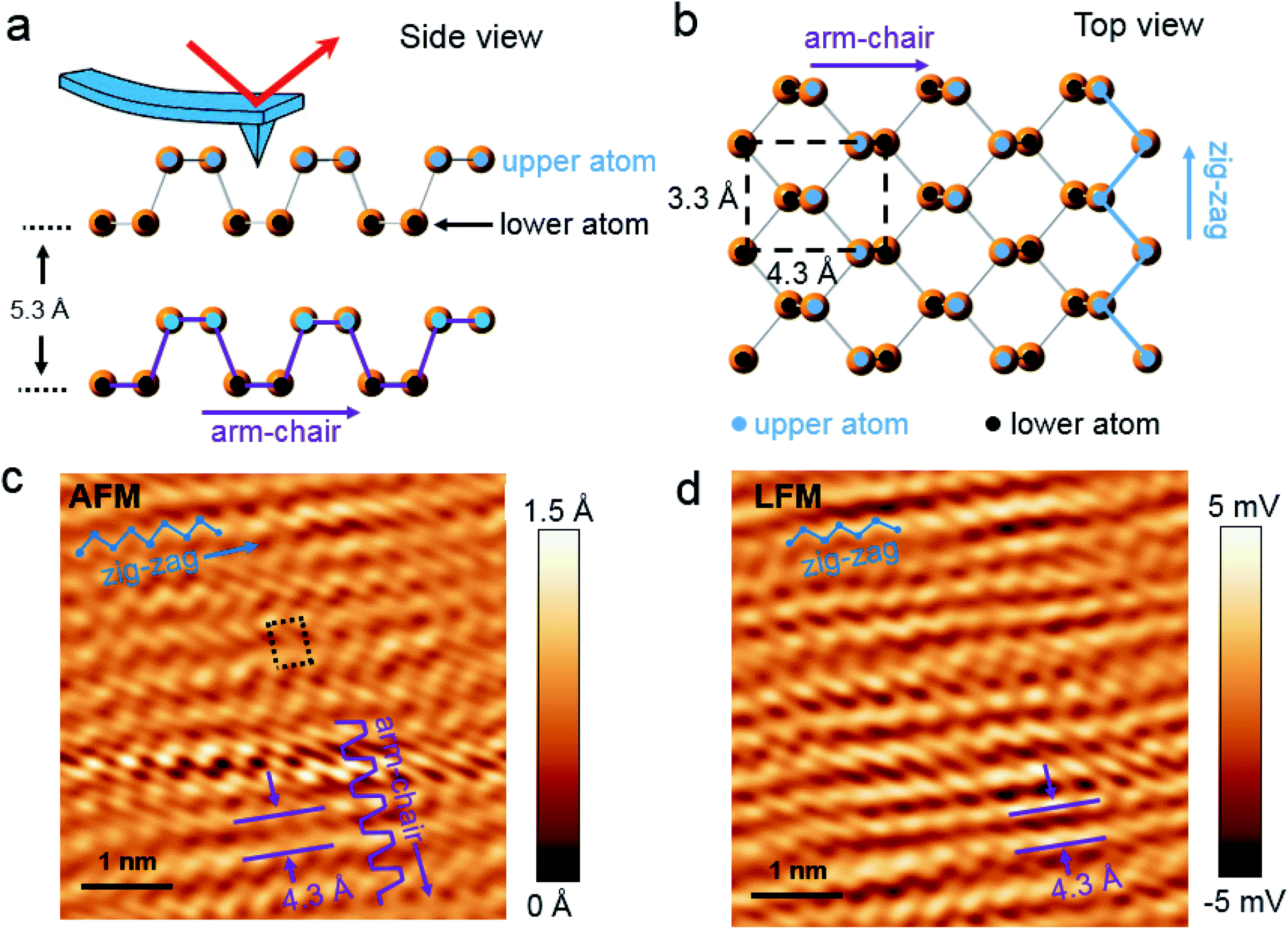 | ||
| Fig. 1 Characterization of freshly cleaved black phosphorus. (a) Side and (b) top views of puckered layered crystal structure of black phosphorus (BP). The interlayer distance is 5.3 Å. The crystal layer has a 4.3 Å periodic armchair pattern and 3.3 Å periodic zig–zag pattern, as indicated by the dashed rectangle in (b). A monolayer of BP is composed of upper atoms (marked by blue dots) and lower atoms (marked by black dots). (c) Atomically resolved atomic force microscopy (AFM) and (d) lateral force microscopy (LFM) images of BP for a scan size of 5 × 5 nm2. Both images show the zig–zag pattern and 4.3 Å periodic armchair structure. The rectangular unit cell of BP is marked by the black dotted line in (c). | ||
After cleaving bulk BP, we characterized the degradation of the BP surface at the atomic scale using our home-built AFM. The measurement environment was maintained at about 18 °C and 35 ± 5% relative humidity. To investigate degradation at the atomic scale immediately after exfoliation, time-dependent frictional images were obtained at the same position with the same frictional scale (−25 to 25 mV), as shown in Fig. 2(a) (30 min), Fig. 2(b) (50 min) and Fig. 2(c) (60 min). The periodic pattern originated from BP armchair in Fig. 2(a) is evident, but the pattern became weaker over time. The fast Fourier transform (FFT) in Fig. 2(d) reveals the 4.3 Å periodicity of the BP armchair pattern in Fig. 2(a)–(c), which is in good agreement with the reported value of a puckered BP monolayer.28 The crystallinity of the BP surface degraded with time, as shown by the amplitude of the FFT (Fig. 2(d)) and frictional profiles (Fig. 2(a)–(c)). This lubrication of BP surface over time was also reported in micro-meter scale.30 Zig–zag patterns on these friction images are less observed than armchair pattern, which implies that degradation speed in zig–zag direction on upper atoms is faster than in armchair direction as suggested by other theoretical group.24,25 The degradation of the exfoliated bulk BP surface in the temperature- and humidity-controlled room was gradual compared with that of other exfoliated BP flakes under ambient conditions.31–33 The slow degradation of BP at lower temperature and humidity was also observed in our temperature- and humidity-controlled cabinet (ESI Fig. S2–S4†). Fig. 2(e) and (f) are serial AFM images at the same area obtained at 60 min and 15 h, respectively, after cleavage. The height profile measured along the dashed line in Fig. 2(e) varies within 1.5 Å (inset of Fig. 2(e)), signaling that the exfoliated BP surface was nearly uniform at 1 h after cleavage. The topographic AFM image measured at 15 h after cleavage without cleaning shows that the BP surface was partially etched. The height profile along the dashed line in Fig. 2(f) shows a step height of about 5 Å, which matches the thickness of a BP monolayer. Right after BP cleavage, BP surface oxides and then gets etched after absorbing near H2O. We measured water contact angles of fresh cleaved BP and environmental aged BP. The water contact angle of fresh cleaved BP surfaces on SiO2/Si substrate reduced by 5–10° after 4 day exposure to ambient conditions (ESI Fig. S5†). It seems that the fresh cleaved BP surface changes from hydrophobic to hydrophilic.21 Fig. 2(f) indicates that water forms isolated clusters and etches the BP surface at random regions. After oxidized BP (e.g., P3O6, P2O5) reacts with water, the etching products will be HxPOy-like species (e.g., H3PO4, H3PO3, H3PO2, H2PO3).23,25 We studied the degradation process using contact mode AFM. There has been many studies of nanometer scale lateral BP etching,31–33 but we have showed in-detail degradation phenomena in lattice-scale. The BP surface can be thinned down layer-by-layer, or even patterned at the nanometer scale, by passing an electric current through it using STM or conductive AFM.34,35 Locally flowing current induces more oxidation on a BP surface, resulting in rapid etching of the BP after absorbing moisture from the surrounding air.34,35 However, we observed that some BP fragments were not oxidized in the etching process, but mixed with the etching product, and the BP crystal fragment revealed when the etching products evaporated. Freshly cleaved BP surface on an Au/Si substrate in a temperature- and humidity-controlled condition showed a relatively uniform surface (ESI Fig. S6†). Fig. 3(a) and (d) are schematic side and top views, respectively, of Fig. 3(b). Part of the cleaved BP surface was covered with etching product over time (Fig. 3(b)); the height of the etching product region increased by about 95 nm (height profile of Fig. 3(b)). Fig. 3(c) shows a current AFM image obtained at 300 mV bias, measured simultaneously with the topography. No current was observed over the etched product, as shown in the current profile (inset of Fig. 3(c)) since a contact mode AFM tip could not penetrate the etched product. We assume that the etched product is mostly frozen concentrated phosphoric acid since the freezing point of concentrated (>85%) phosphoric acid is around 18 °C.36 After 10 h from etching process, we simultaneously re-obtained the topography (Fig. 3(f)) and current (Fig. 3(g)) AFM images at the same position as Fig. 3(b) at 300 mV bias. The height profile along the dashed line in Fig. 3(f) shows a two-layer BP terrace with a 0.5 nm (corresponding to BP monolayer thickness) step height (inset of Fig. 3(f)). The current profile measured along the dashed line in Fig. 3(g) reveals that the BP terraced region had the same order of conductivity as the pristine BP region. Schematic side (Fig. 3(e)) and top (Fig. 3(h)) views of Fig. 3(b) highlight the mono and bi-layer phosphorene. High resolution frictional images of a 4.5 × 4.5 nm2 region of the pristine BP area (“I” position in Fig. 3(f)) and the BP fragment (“J” position in Fig. 3(f)) regions are shown in Fig. 3(i) and (j), respectively. High-resolution LFM images show that the both substrate and terraced BP regions have the same armchair arrangement. The frictional profile along the dashed line in Fig. 3(j) shows a five periodic pattern, indicating that the terraced 2D phosphorene had a repeating pattern of about 4.2 Å. This is in good agreement with the 4.3 Å periodic armchair pattern for crystalline BP.
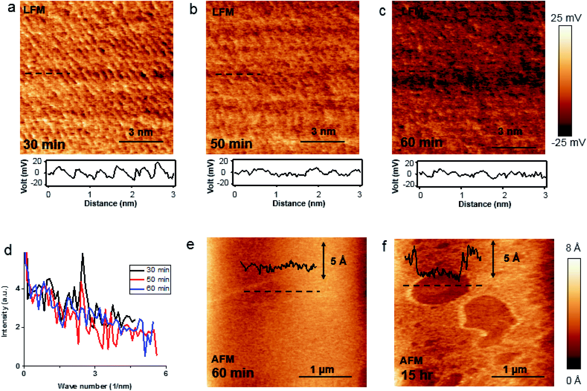 | ||
| Fig. 2 Atomic-scale degradation of cleaved black phosphorus. (a–c) Lateral force microscopy images of BP at 30 min (a), 50 min (b), and 60 min (c) after cleavage. (d) Fast Fourier Transform (FFT) spectral intensity of (a–c) images. (e and f) AFM images of BP at 60 min (e) and 15 h (f) after cleavage at the same position. Insets: height profiles along the dashed lines. | ||
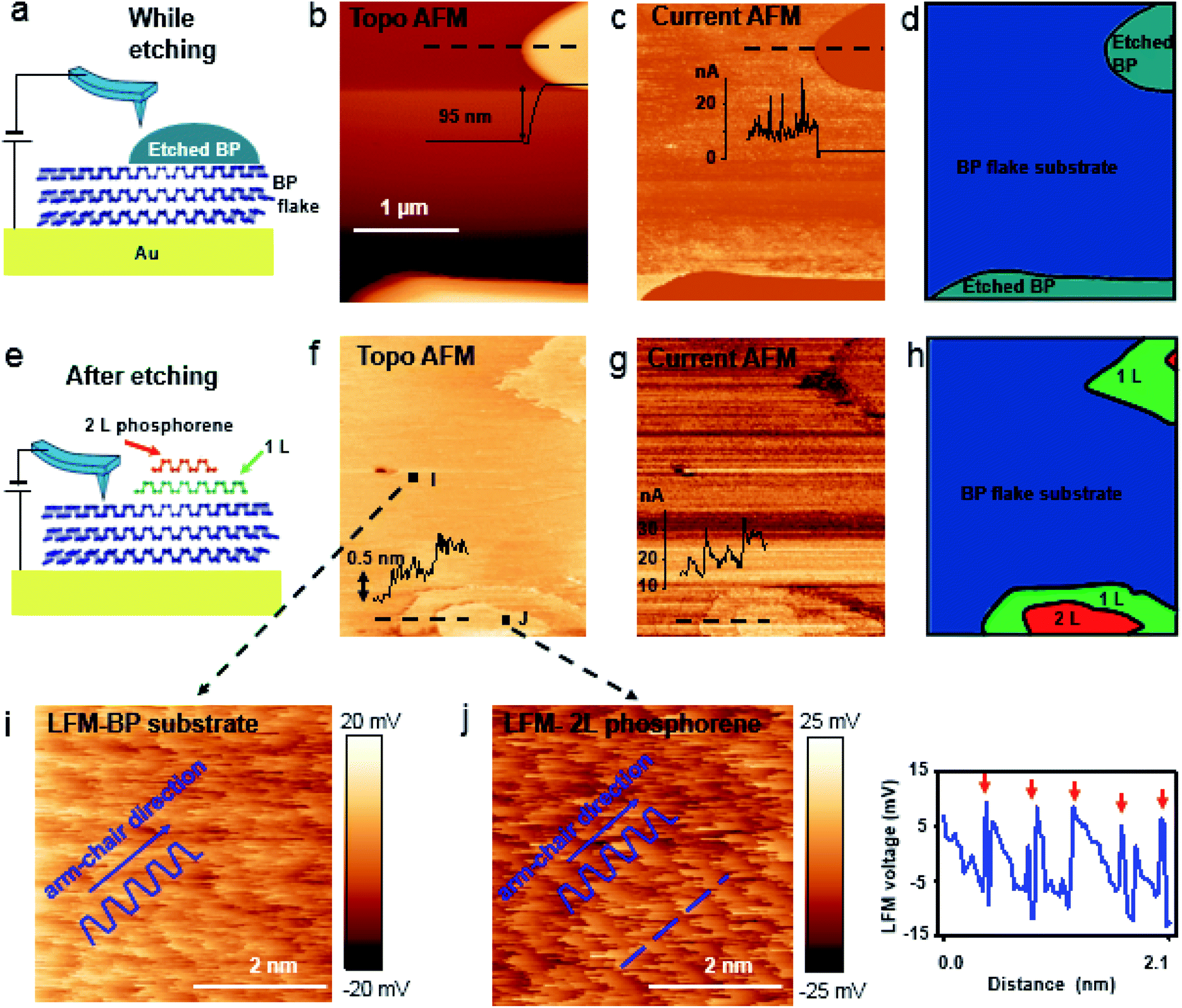 | ||
| Fig. 3 A thin layer of black phosphorus after voltage-assisted BP etching. (a) Schematic side view of BP etched by conductive AFM tip. (b–d) Simultaneously measured topographical AFM image (b), conductive AFM image (c) and schematic top view (d) while applying a bias voltage of 300 mV. Inset in (b): height profile along the dashed line. Inset in (c): current profile along the dashed line. (e) Schematic side view of terraced BP after etching. (f–h) Simultaneously measured topographical AFM image (f) and conductive AFM image (g) of the same area as (b), and schematic top view (h) after etching. Inset in (f): height profile along the dashed line. Inset in (g): current profile along the dashed line. (i) LFM image measured at the BP substrate region (position I) in (f) for a scan size of 4.5 × 4.5 nm2. (j) LFM image measured at the terraced BP region (position J) in (f) for a scan size of 4.5 × 4.5 nm2. Right image shows the LFM profile along the blue dashed line. | ||
We used Raman spectroscopy and AFM to scrutinize the crystalline BP structure after voltage-assisted etching. A BP flake, prepared on an Au/Si substrate (Fig. 4(a)), was scanned at a bias voltage of 4 V using conductive AFM, and then it was imaged using a charge-coupled device (CCD) after 3 h (ESI Fig. S7(b)†) and 15 days (Fig. 4(b)). The inset of Fig. 4(b) shows a schematic map of the original BP region in blue, and the expanded BP region after etching in orange. Fig. 4(c) schematically shows the scan direction of the tip and the BP surface before and after the etching. When a bias voltage of ∼4 V was applied to the BP on an Au/Si substrate through an AFM tip, etching of the BP occurred around the AFM tip, and the BP etching product region increased (ESI Fig. S8(c)†). The intensity of the A2g Raman mode, obtained over the dashed rectangle in Fig. 4(b), is mapped in Fig. 4(d). The spectrum acquired at the “B” position in Fig. 4(d) confirms the crystalline BP, but not at the “A” position (Fig. 4(e)). This result demonstrates that voltage-assisted BP etching on the Au/Si substrate can produce BP fragments. A frictional image measured at the “F” position, indicated by the red square in Fig. 4(b), shows an armchair pattern with the periodicity of 4.3 Å (Fig. 4(f)). The quality of the frictional image is not as good as prior frictional images since 4 V of high voltage etching produces multi-layer BP with possible low degree of crystallinity. The inset in Fig. 4(f) is the frictional profile measured along the dashed line in Fig. 4(f). The frictional profile shows six bumps over the 2.6 nm-long dashed line. This pattern is in good agreement with the 4.3 Å periodic armchair arrangement of the BP crystal. The crystal structure details from the AFM images and Raman spectra confirmed that voltage-assisted rapid BP etching can produce a few layer of BP fragments.
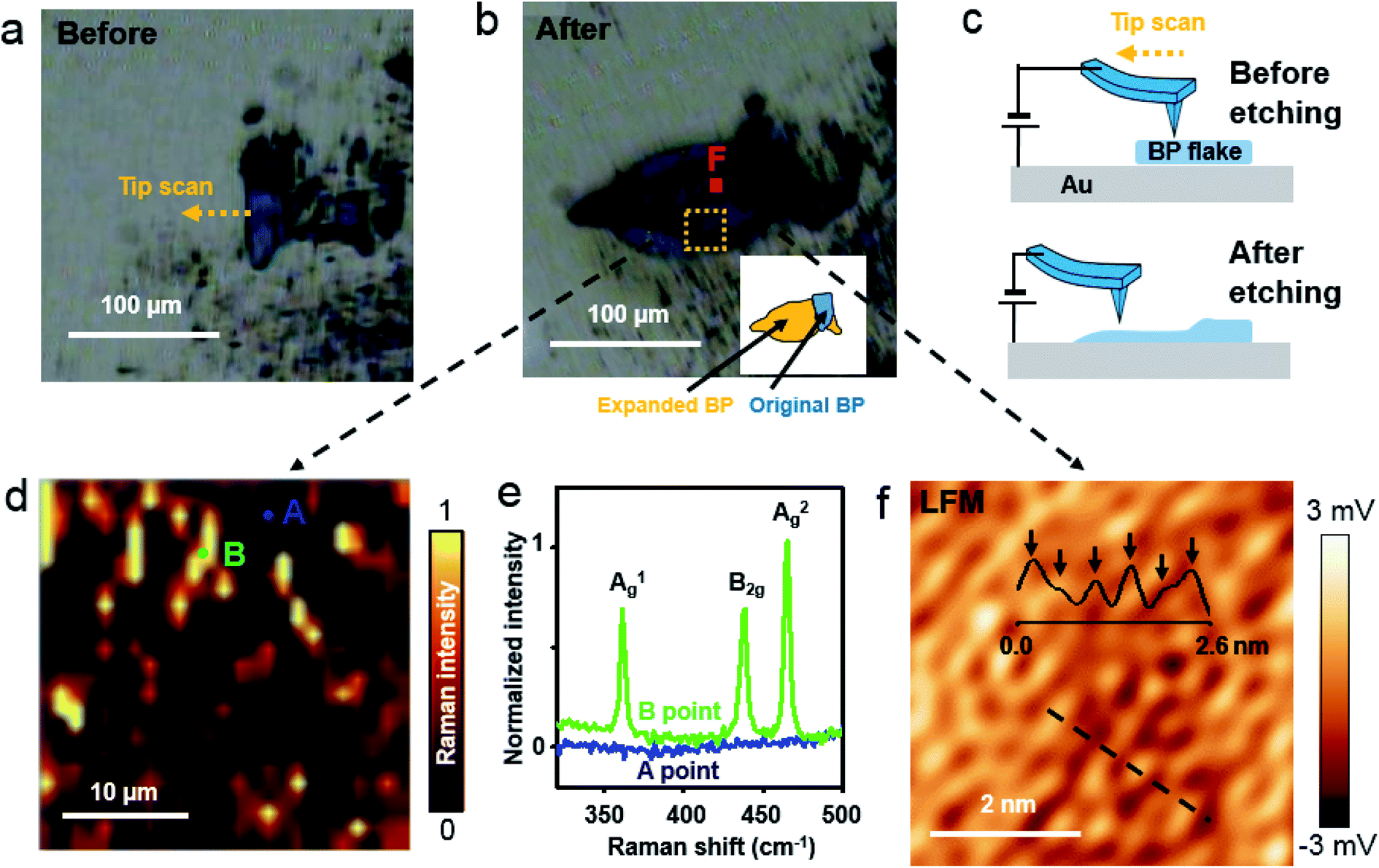 | ||
| Fig. 4 Characterization of black phosphorus after voltage-assisted etching. (a and b) Optical microscopy images of BP before (a) and after (b) tip-assisted etching with 4 V bias voltage. (c) Schematic diagram before (top) and after (bottom) etching. (d) Intensity of the A2g Raman mode measured in the dashed rectangle of (c). (e) Raman spectra taken at the A and B locations in (d). Spectra are normalized to the A2g peak. (f) LFM image measured at the red F point in (c) for a scan size of 5 × 5 nm2. Inset: LFM profile along the black dashed line. | ||
The effect of the voltage-assisted BP etching was studied by conducting the same types of experiments at a pressure of about 10−1 torr. We attempted to etch a BP flake by dragging a tip biased at 5 V. Ex situ Raman spectra acquired around the BP etching region show that the expanded BP region was continuous, without non-crystalline region (ESI Fig. S9(b)† and the middle panel of Fig. S8(c)†), which contrasts with the island-like crystalline BP in Fig. 4(d) since most BP did not oxidize in the voltage-assisted etching process due to lack of oxygen and water under vacuum. The height profile (at the top of ESI Fig. S9(c)†) around the etched BP confirms that the etching process developed at the tip. The intensity ratio of the A1g to A2g Raman modes (at the bottom of ESI Fig. S9(c)†) of the fabricated BP region under vacuum is more than 0.55, which confirms that the formed BP was not mostly affected by oxidation under vacuum.15,31
Conclusions
We characterized the atomic structure of the exfoliated BP surface using AFM in a temperature- and humidity-controlled condition. High-resolution AFM images of the BP surface revealed zig–zag chains and a 4.3 Å periodic armchair pattern of the BP crystal lattice. Frictional LFM profiles showed that the intensity of the armchair-related LFM signal deteriorated slowly in the temperature- and humidity-controlled room, and high-resolution topological AFM images taken simultaneously with LFM images revealed that the BP surface preferred lateral etching to vertical etching. Applying voltage to a BP surface using a conductive AFM tip induced rapid BP etching, which could produce a few layer of BP fragments. We believe that these atomic scale studies of BP can provide the insight over BP-based 2D electronics.Conflicts of interest
There are no conflicts to declare.Acknowledgements
This work was supported by National Research Foundation of Korea (NRF-2016R1D1A1B01011181 and National Honor Scientist Program: 2010-0020414). G. H. L acknowledges supports by the Basic Science Research Program through the National Research Foundation of Korea (NRF) funded by the Ministry of Science, ICT, and Future Planning (2018M3D1A1058794), and the Korea Institute of Energy Technology Evaluation and Planning (KETEP) and the Ministry of Trade, Industry, and Energy (MOTIE) of the Republic of Korea (No. 20173010013340) and Creative-Pioneering Researchers Program through Seoul National University (SNU).References
- S. Z. Butler, S. M. Hollen, L. Y. Cao, Y. Cui, J. A. Gupta, H. R. Gutierrez, T. F. Heinz, S. S. Hong, J. X. Huang, A. F. Ismach, E. Johnston-Halperin, M. Kuno, V. V. Plashnitsa, R. D. Robinson, R. S. Ruoff, S. Salahuddin, J. Shan, L. Shi, M. G. Spencer, M. Terrones, W. Windl and J. E. Goldberger, ACS Nano, 2013, 7, 2898–2926 CrossRef CAS PubMed.
- Q. H. Wang, K. Kalantar-Zadeh, A. Kis, J. N. Coleman and M. S. Strano, Nat. Nanotechnol., 2012, 7, 699–712 CrossRef CAS PubMed.
- M. Chhowalla, H. S. Shin, G. Eda, L. J. Li, K. P. Loh and H. Zhang, Nat. Chem., 2013, 5, 263–275 CrossRef PubMed.
- H. H. Churchill and P. Jarillo-Herrero, Nat. Nanotechnol., 2014, 9, 330–331 CrossRef CAS PubMed.
- H. Liu, Y. C. Du, Y. X. Deng and P. D. Ye, Chem. Soc. Rev., 2015, 44, 2732–2743 RSC.
- H. Liu, A. T. Neal, Z. Zhu, Z. Luo, X. F. Xu, D. Tomanek and P. D. Ye, ACS Nano, 2014, 8, 4033–4041 CrossRef CAS PubMed.
- S. Zhang, J. Yang, R. J. Xu, F. Wang, W. F. Li, M. Ghufran, Y. W. Zhang, Z. F. Yu, G. Zhang, Q. H. Qin and Y. R. Lu, ACS Nano, 2014, 8, 9590–9596 CrossRef CAS PubMed.
- F. N. Xia, H. Wang and Y. C. Jia, Nat. Commun., 2014, 5, 4458 CrossRef CAS PubMed.
- V. Tran, R. Soklaski, Y. F. Liang and L. Yang, Phys. Rev. B: Condens. Matter Mater. Phys., 2014, 89, 235319 CrossRef.
- Y. Q. Cai, G. Zhang and Y. W. Zhang, Sci. Rep., 2014, 4, 6677 CrossRef CAS PubMed.
- P. W. Bridgman, J. Am. Chem. Soc., 1914, 36, 1344–1363 CrossRef CAS.
- A. Brown and S. Rundqvist, Acta Crystallogr., 1965, 19, 684–685 CrossRef CAS.
- S. H. Aldave, M. N. Yogeesh, W. N. Zhu, J. Kim, S. S. Sonde, A. P. Nayak and D. Akinwande, 2D Mater., 2016, 3, 014007 CrossRef.
- L. K. Li, Y. J. Yu, G. J. Ye, Q. Q. Ge, X. D. Ou, H. Wu, D. L. Feng, X. H. Chen and Y. B. Zhang, Nat. Nanotechnol., 2014, 9, 372–377 CrossRef CAS PubMed.
- D. Hanlon, C. Backes, E. Doherty, C. S. Cucinotta, N. C. Berner, C. Boland, K. Lee, A. Harvey, P. Lynch, Z. Gholamvand, S. F. Zhang, K. P. Wang, G. Moynihan, A. Pokle, Q. M. Ramasse, N. McEvoy, W. J. Blau, J. Wang, G. Abellan, F. Hauke, A. Hirsch, S. Sanvito, D. D. O'Regan, G. S. Duesberg, V. Nicolosi and J. N. Coleman, Nat. Commun., 2015, 6, 8563 CrossRef CAS PubMed.
- P. Yasaei, B. Kumar, T. Foroozan, C. H. Wang, M. Asadi, D. Tuschel, J. E. Indacochea, R. F. Klie and A. Salehi-Khojin, Adv. Mater., 2015, 27, 1887–1892 CrossRef CAS PubMed.
- J. R. Brent, A. K. Ganguli, V. Kumar, D. J. Lewis, P. D. McNaughter, P. O'Brien, P. Sabherwal and A. A. Tedstone, RSC Adv., 2016, 6, 86955–86958 RSC.
- S.-Y. Lei, H.-Y. Shen, Y.-Y. Sun, N. Wan, H. Yu and S. Zhang, RSC Adv., 2018, 8, 14676–14683 RSC.
- Y. Abate, Adv. Mater., 2018, 30, 1704749 CrossRef PubMed.
- W. Gaoxue, J. S. William, P. Ravindra and P. K. Shashi, 2D Mater., 2016, 3, 025011 CrossRef.
- Y. Huang, J. Qiao, K. He, S. Bliznakov, E. Sutter, X. Chen, D. Luo, F. Meng, D. Su, J. Decker, W. Ji, R. S. Ruoff and P. Sutter, Chem. Mater., 2016, 28, 8330–8339 CrossRef CAS.
- G. Abellan, S. Wild, V. Lloret, N. Scheuschner, R. Gillen, U. Mundloch, J. Maultzsch, M. Varela, F. Hauke and A. Hirsch, J. Am. Chem. Soc., 2017, 139, 10432–10440 CrossRef CAS PubMed.
- J. Plutnar, Z. Sofer and M. Pumera, ACS Nano, 2018, 12, 8390–8396 CrossRef CAS PubMed.
- A. Ziletti, A. Carvalho, D. K. Campbell, D. F. Coker and A. H. Castro Neto, Phys. Rev. Lett., 2015, 114, 046801 CrossRef CAS PubMed.
- W. Gaoxue, J. S. William, P. Ravindra and P. K. Shashi, 2D Mater., 2016, 3, 025011 CrossRef.
- A. Ziletti, A. Carvalho, P. E. Trevisanutto, D. K. Campbell, D. F. Coker and A. H. C. Neto, Phys. Rev. B: Condens. Matter Mater. Phys., 2015, 91, 085407 CrossRef.
- Y. L. Du, C. Y. Ouyang, S. Q. Shi and M. S. Lei, J. Appl. Phys., 2010, 107, 093718 CrossRef.
- C. D. Zhang, J. C. Lian, W. Yi, Y. H. Jiang, L. W. Liu, H. Hu, W. D. Xiao, S. X. Du, L. L. Sun and H. J. Gao, J. Phys. Chem. C, 2009, 113, 18823–18826 CrossRef CAS.
- D. R. Baselt and J. G. Baldeschweiler, J. Vac. Sci. Technol., B: Microelectron. Nanometer Struct.--Process., Meas., Phenom., 1992, 10, 2316–2322 CrossRef CAS.
- S. Wu, F. He, G. Xie, Z. Bian, J. Luo and S. Wen, Nano Lett., 2018, 18, 5618–5627 CrossRef CAS PubMed.
- A. Favron, E. Gaufres, F. Fossard, A. L. Phaneuf-L'Heureux, N. Y. W. Tang, P. L. Levesque, A. Loiseau, R. Leonelli, S. Francoeur and R. Martel, Nat. Mater., 2015, 14, 826–832 CrossRef CAS PubMed.
- A. Castellanos-Gomez, L. Vicarelli, E. Prada, J. O. Island, K. L. Narasimha-Acharya, S. I. Blanter, D. J. Groenendijk, M. Buscema, G. A. Steele, J. V. Alvarez, H. W. Zandbergen, J. J. Palacios and H. S. J. van der Zant, 2D Mater., 2014, 1, 025001 CrossRef.
- H. Kwon, S. W. Seo, T. G. Kim, E. S. Lee, P. T. Lanh, S. Yang, S. Ryu and J. W. Kim, ACS Nano, 2016, 10, 8723–8731 CrossRef CAS PubMed.
- S.-L. Yau, T. P. Moffat, A. J. Bard, Z. Zhang and M. M. Lerner, Chem. Phys. Lett., 1992, 198, 383–388 CrossRef CAS.
- X. L. Liu, K. S. Chen, S. A. Wells, I. Balla, J. Zhu, J. D. Wood and M. C. Hersam, Adv. Mater., 2017, 29, 1604121 CrossRef PubMed.
- W. H. Ross and R. M. Jones, J. Am. Chem. Soc., 1925, 47, 2165–2170 CrossRef CAS.
Footnote |
| † Electronic supplementary information (ESI) available. See DOI: 10.1039/c9ra08029e |
| This journal is © The Royal Society of Chemistry 2020 |