
 Open Access Article
 This Open Access Article is licensed under a Creative Commons Attribution-Non Commercial 3.0 Unported Licence
Continuous-wave laser annealing of metallic layers for CuInSe2 solar cell applications: effect of preheating treatment on grain growth†
Panagiota Arnou *a,
Alberto Lomuscioa,
Thomas P. Weissa,
Daniel Siopaa,
Sergio Giraldob,
Edgardo Saucedob,
Michael A. Scarpullac and
Phillip J. Dale*a
*a,
Alberto Lomuscioa,
Thomas P. Weissa,
Daniel Siopaa,
Sergio Giraldob,
Edgardo Saucedob,
Michael A. Scarpullac and
Phillip J. Dale*a
aPhysics and Materials Science Research Unit, University of Luxembourg, L-4422 Belvaux, Luxembourg. E-mail: phillip.dale@uni.lu
bCatalonia Institute for Energy Research (IREC), Spain
cMaterials Science and Engineering, University of Utah, Salt Lake City, Utah, USA
First published on 2nd January 2020
Abstract
Ultra-fast thermal annealing of semiconductor materials using a laser can be revolutionary for short processing times and low manufacturing costs. Here we investigate Cu–In–Se thin films as precursors for CuInSe2 semiconductor absorber layers via laser annealing. The reaction mechanism of laser annealed metal stacks is revealed by measuring ex situ X-ray diffractograms, Raman spectra and composition. It is shown that the formation of CuInSe2 occurs via the formation of CuxSe/InxSey binary phases as in conventional annealing routes, despite the entirely different annealing time scale. Pre-alloying the Cu and In metals prior to laser annealing significantly enhances the selenisation reaction rate. Laser annealing for six seconds approaches a near phase-pure material, which exhibits similar crystalline quality to the reference material annealed for ninety minutes in a tube furnace. The estimated quasi Fermi level splitting deficit for the laser annealed material is only 60 meV lower than the reference sample, which implies a high optoelectronic quality.
Introduction
Despite ongoing progress in photovoltaic (PV) material development, PV module manufacturing processes with lower costs and higher throughput are necessary to make this a more widespread technology in the energy production market. Thin film PV devices contain compound semiconductor absorber layers, which have to be annealed at high temperatures for several minutes to hours in order to exhibit the appropriate opto-electronic properties. One way to increase throughput is to move from conventional resistive annealing of the substrate and absorber layer to laser annealing (LA) of the absorber layer only. As well as shorter annealing times and compatibility with in-line manufacturing, LA can have a lower energy input cost when compared to conventional furnace annealing.1 Further, LA offers localised heating which would enable higher reaction temperatures on temperature sensitive substrates, such as polyimide foils. This becomes increasingly attractive in terms of continuous processing, as it can be applied in roll-to-roll processing of flexible substrates. High throughput and low-cost deposition methods can also be implemented in these processes, such as electrodeposition or printing.2Cu(In,Ga)(Se,S)2 (CIGS) and the related alloys are used as absorber layers in PV devices, and produce the highest power conversion efficiencies (exceeding 23%) of all inorganic thin film technologies.3,4 The record devices contain CIGS thin films that are synthesised by thermally heating stacked metal layered precursors. The thermal annealing process is typically performed in chalcogen atmosphere in a furnace.5,6 Here, we investigate these solid state and gas/solid reactions with LA, which take place on a two orders of magnitude faster time scale. The aim of this work is to understand the effect of ultra-fast annealing on the reaction pathway of LA metal stacked precursors, which may differ to conventional annealing routes. By identifying the reaction pathway we provide access to a new kinetic regime for fast annealing routes and we assess the potential of this approach for thin film solar cell materials.
In previous work, we demonstrated the potential of this approach by performing LA on a CuInSe2 (CIS) precursor which was electrodeposited with all elements in a single step at room temperature. These precursors consist of a single layer with all the elements intimately mixed in an amorphous/highly nano-crystalline state. LA induced crystallisation to produce 200 nm sized grains on a time scale of only 1 s. The LA absorbers could be converted into first working devices with a 23 mA cm−2 short circuit current.7 Nonetheless, the material showed lateral non-uniform properties, which largely originated from the precursor deposition step.
Having shown the potential of LA for co-deposited CIS, here we focus on a stacked elemental layer precursor which can be made laterally uniform and is more industrially relevant.8 LA of metal stacks for CIS formation has been proven to be rather challenging, due to Se loss and dewetting of the absorber from the substrate.1 Further, metal stacked precursors exhibit a strong elemental gradient, as opposed to the co-deposited material with intimately mixed elements. The requirement for a significant elemental interdiffusion in addition to the grain growth adds a factor of complexity in this approach. Previous work on metal precursors used a Se/Cu/In metal stacked configuration and a continuous wave (CW) argon-ion laser (λ = 457.9 to 514.5 nm). However, no opto-electronic characterisation has been reported, due to strong Se loss at the temperatures reached during LA at that setup.9,10 Preliminary work from our group using a 1064 nm CW laser on Cu/In/Se samples showed a large amount of secondary phases by XRD and a lack of clear evidence of CIS formation.7 This was attributed to insufficient annealing temperature reached for elemental diffusion and reaction to occur, as well as the Se loss.7
The reaction mechanism for selenising stacked metal precursors in a tube furnace11 or in a rapid thermal processing (RTP) oven12 has been investigated. In both cases there are a series of intermediate reactions taking place, with the binary chalcogenide phases being formed first, before reacting together to form CIS. For the case of the tube furnace annealing, co-sputtering of Cu/In was found to be beneficial to achieve complete mixing of the metals in the precursor film.11 Similarly, a mild heating step can also be implemented to effectively alloy the stacked layers prior to selenisation. This “pre-alloying step” was shown to improve the metal distribution in the precursor, thereby enhancing the grain growth in the subsequent reactive annealing step.13 The pre-alloying step was also found to suppress side reactions which would otherwise lead to poor crystallinity in the final film.14 Specifically in non-prealloyed films, In2Se3 reacted with liquid Se at 200 °C, resulting in large Se loss from the film and eventually film delamination.14
Modelling of the optical absorption for the Cu/In/Se stacked precursor showed that the laser beam power (for 1 s annealing time) is dissipated within a narrow region at the surface of the In metal, with >80% of the irradiation being reflected.7 Here, we increase the annealing time in order to form binary or ternary phases which would better absorb the radiation and consequently result in higher temperatures during LA. We investigate the reaction mechanism for LA Cu/In stacked metal precursors, by performing ex situ XRD, Raman and composition measurements. We show that by implementing a pre-alloying step prior to LA, the elemental gradient in the film is largely removed, which significantly increases the reaction rate during LA. The effect of pre-alloying step in LA is demonstrated for the first time and it is shown to significantly improve the final material properties. We compare these findings with a reference sample which has been annealed in a tube furnace for >90 min and we show that the two materials can exhibit very similar crystallinity and opto-electronic quality.
Results
We first report structural characterisation results of the precursor layers followed by the characterisation of the annealed samples, in order to observe changes induced by LA. In a second step in the Discussion section, we discuss the results and propose a growth model for the LA stacked elemental precursor layers. A complete description of the experimental processes and the sample information are given in the Experimental section. A brief summary of the processed samples is presented in Table 1, including the naming system used in the remaining of the manuscript. Briefly, the samples are named based on the annealing dwell time, with LA times of 2, 4 and 6 s. Also, samples that have undergone a preheating step prior to LA are prefixed with “PR”. The preheating step was included to investigate the effect of pre-alloying the precursors on the reaction completion and the final material quality. All precursors for LA were deposited with the appropriate metal thicknesses, aiming for a final thickness of 0.5 μm after annealing (assuming a complete reaction). Separately, two samples were used as reference, which were annealed inside a tube furnace and with a heating time of 90 min. Two different thicknesses were used for the reference samples, which will be denoted as “thin” and “thick”. All the Cu/In precursor samples are capped with a Se layer prior to LA.| Deposition method | Targeted thickness (μm) | Annealing time | Name | Name of preheated |
|---|---|---|---|---|
| Electro-deposition | >0.5 | 2 s | ED-LA 2 s | ED-PR-LA 2 s |
| 6 s | ED-LA 6 s | ED-PR-LA 6 s | ||
| Vacuum | 0.5 | 0 (precursor) | Thin | Thin PR |
| 2 s | LA-2 s | LA-PR 2 s | ||
| 4 s | LA-4 s | LA-PR 4 s | ||
| 6 s | LA-6 s | LA-PR 6 s | ||
| 90 min (ref) | Thin oven | Thin PR oven | ||
| 1.0 | 0 (precursor) | Thick | Thick PR | |
| 90 min (ref) | Thick oven | Thick PR oven |
Precursor characterisation
SEM imaging was performed to investigate the morphology of the precursor films. Fig. 1a shows the top-view image of the as-deposited thin Cu/In precursor which consists of 2–3 micron laterally-sized In islands on top of a compact layer, which contains Cu and In. Fig. 1b shows the morphology of the precursor after the pre-alloying step, where the In islands are removed to a large extent, forming a smoother layer. Fig. 1c shows a cross sectional image of the as-deposited precursor (no prealloying step), with the Se capping layer. Indium islands are visible on top of a thin compact layer, and a uniform conformal Se coating is on top. Fig. 1d and e show the corresponding top view image of an uncapped electrodeposited precursor and a cross sectional image with Se capping. A similar morphology is observed as in the vacuum-deposited samples, with ∼300 nm total thickness of the Cu/In layers.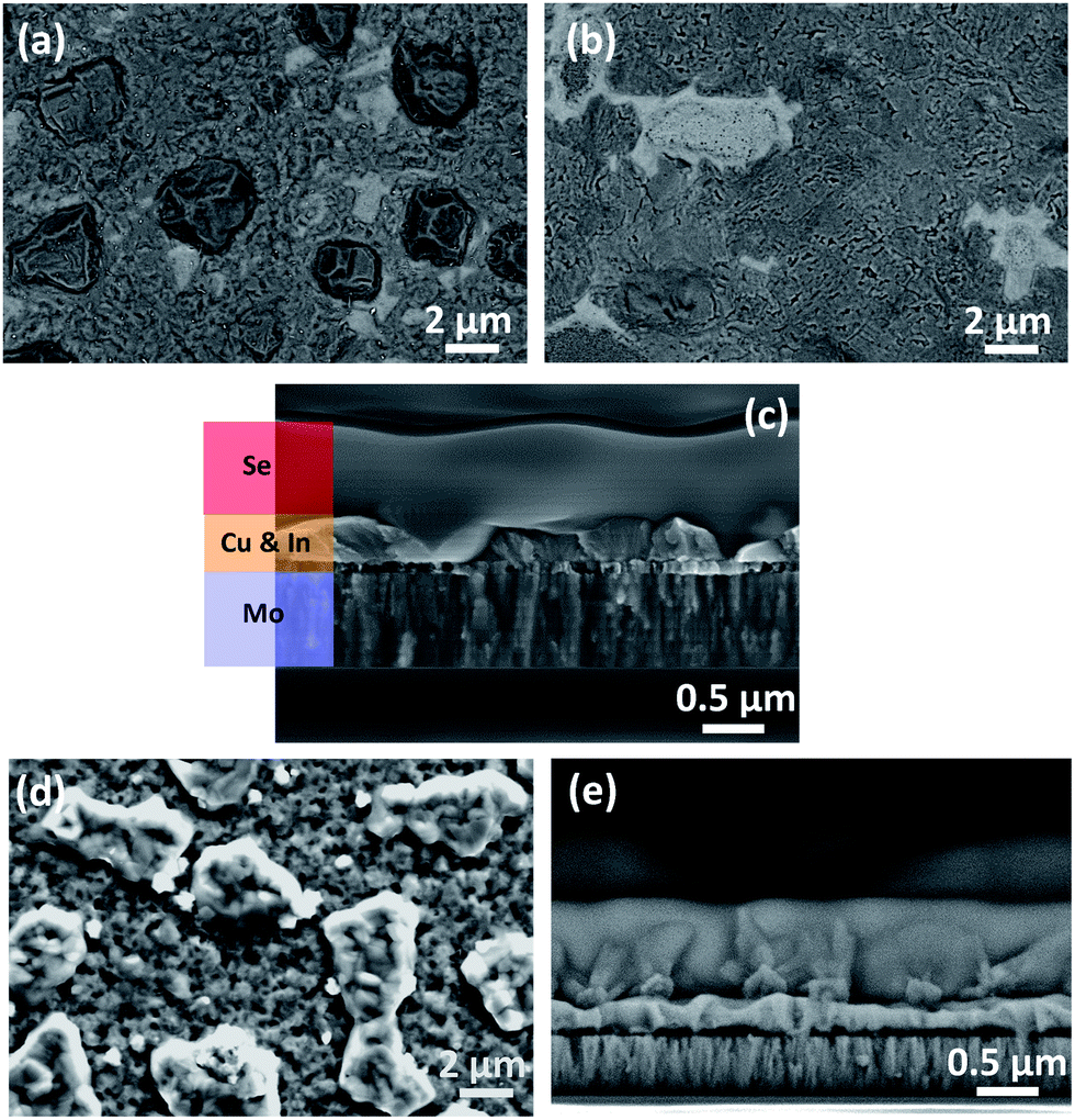 | ||
| Fig. 1 SEM images of the precursor samples: top view image of thin Cu/In layers in the as-deposited state (a) and after the pre-alloying step (b). (c) Cross sectional image of Cu/In/Se thin precursor with each layer indicated, (d) top view image of Cu/In thin-ED precursor, (e) cross sectional image of Cu/In/Se thin-ED precursor. | ||
XRD measurements were performed on the precursor samples for bulk phase identification (Fig. 2). The diffractogram of the uncapped thin precursor sample (red) shows only peaks that are assigned to In (green markers) and the metastable CuIn (pink markers) and Cu2In (grey markers) phases.15,16 The XRD pattern of the thick precursor sample (black) also shows peaks assigned to Cu (brown marker). The XRD pattern of the thin precursor after Se capping is also included (blue) to confirm the absence of the CIS phase (dotted vertical line indicates the position of the expected 112 peak of chalcopyrite structure). The identical pattern in the capped and uncapped precursor sample confirms that the Se capping process does not alter the precursor and does not cause any side reactions. Finally, the XRD pattern of the thin precursor after pre-alloying step (thin PR, green) is also included for comparison. It can be observed that the CuIn and Cu2In minor peaks are removed, and new peaks assigned to the Cu11In9 alloy have appeared, which is the thermodynamically preferred phase.17
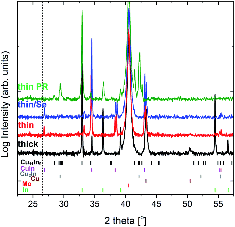 | ||
| Fig. 2 XRD diffractograms for the thick precursor (black), the thin precursor (red), the thin precursor with the Se cap (blue) and the thin uncapped precursor after pre-alloying (green). The dotted vertical line indicates the expected position of 112 of CuInSe2 chalcopyrite structure. | ||
Characterisation of LA samples
LA has been performed on Cu/In/Se precursor samples, with the laser flux kept constant at 150 W cm2 and a varied dwell time of 2, 4 and 6 s. Two sets of samples, as-deposited and pre-alloyed, have been annealed using identical conditions. Fig. 3 summarises representative top-view SEM images for each sample and at each LA dwell time. Na2S etching was performed on the samples prior to imaging, to remove any unreacted selenium from the surface. As a first observation, the morphology of all the LA-samples appears to be significantly different to the precursor samples, indicating that a reaction has occurred between the selenium and metal layers. The sample appearance also seems to be different between the pre-alloyed samples and their non-pre-alloyed counterparts. The LA-2 s sample appears to have a two layer structure, with small grains scattered on the surface and larger grains underneath. The pre-alloyed sample consists of smaller grains, but appears to be denser. With regards to the LA-4 s samples, the non-prealloyed film retains the small grains, but the pre-alloyed film appears to be more crystallised. Different grain morphologies are observed on the surface of the 6 s samples, suggesting the presence of secondary phases. EDS point analysis on different features of the 6 s LA films (not shown) shows higher In content on the smaller grains, which implies the presence of In-rich secondary phases on the surface. Top-view and cross sectional images are also included for the reference sample (thick oven). It appears that the absorber is fully recrystallised throughout the bulk but the lateral grain size is smaller (up to 300 nm), irrespective of the pre-alloying step. These small grain sizes (<500 nm) are typically seen in CIS films with Cu-poor composition.18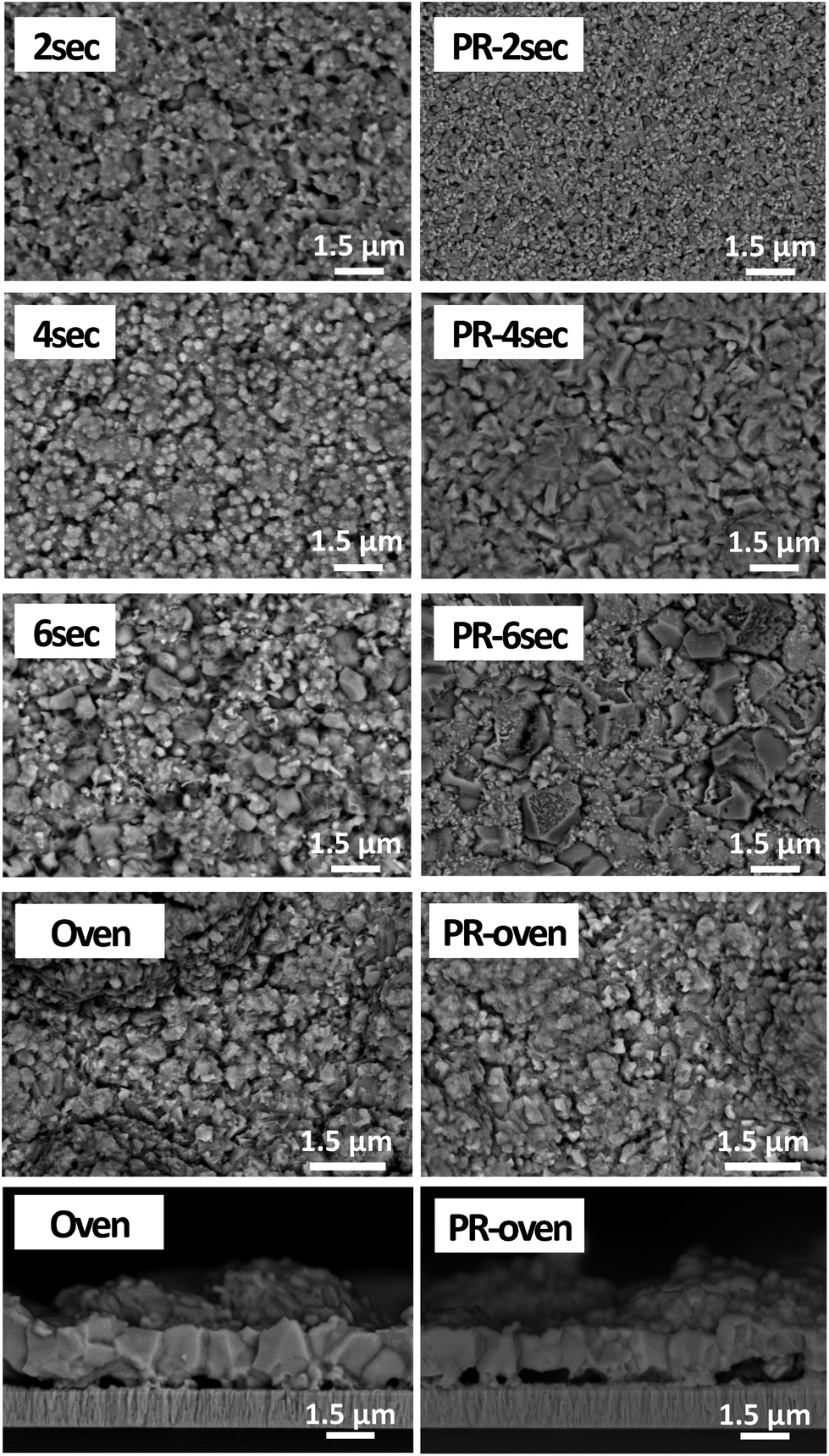 | ||
| Fig. 3 SEM images of the annealed samples. Top-view images of LA samples annealed for 2, 4, and 6 s, with and without the pre-alloying step. The top view and cross sectional images of the reference material (thick oven) are also included for comparison. | ||
The composition of each annealed sample was determined by area analysis with EDS, at 1.5k magnification and 20 kV accelerating voltage. At these measurement conditions the measured composition should sample all the absorber and a small part of the underlying molybdenum, as the depth of measurement is expected to be in the micrometer range. The effect of LA dwell time on the apparent composition of the absorber films is summarised in Fig. 4. The Cu/In ratio is progressively increased with the dwell time, until at 6 s the ratio is the same as the oven annealed sample (thin oven) of ∼0.8. It should be noted that the Cu/In ratio of the thick oven sample was 0.9. This difference is likely related to a slightly different metal thicknesses ratio between the two samples. The dotted lines in Fig. 4 represent the composition of the “thin oven” reference sample for a more consistent comparison, since the precursor has the same thickness with the precursors used for LA. Due to the shape of the X-ray excitation volume in the sample,19 the apparent composition obtained by EDS is expected to be more representative of the front of the sample and less so at the back. Therefore, the low Cu content in 2 and 4 s LA samples gives an indication of a strong compositional grading in the film, with some unreacted Cu still present at the back. The oven annealed sample with a heating time of 90 min will have no metal composition gradient. The same Cu content between the 6 s LA sample and the oven annealed reference indicates better elemental intermixing, which implies a complete reaction.
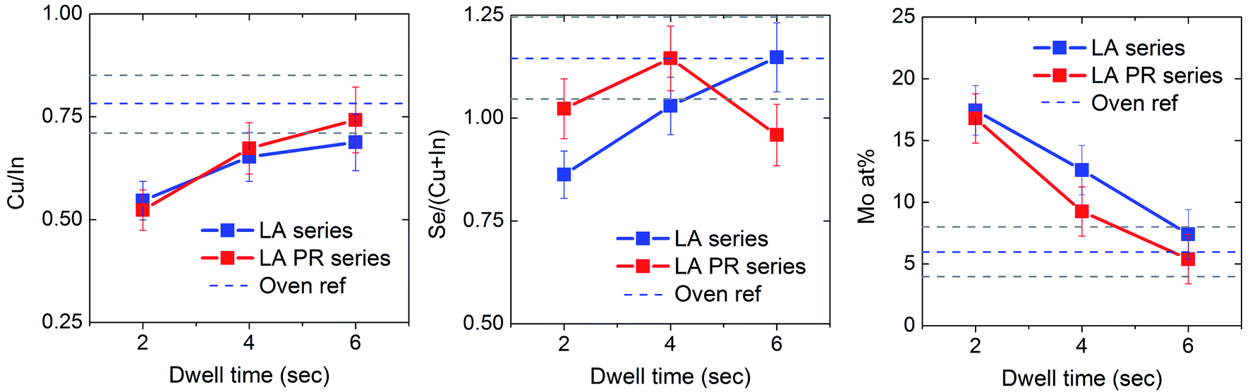 | ||
| Fig. 4 Summary of the composition of each sample set (with and without pre-alloying) with respect to the LA dwell time, as obtained by EDS. The dotted lines (blue) represent the composition of the reference material (thin oven) within error (grey lines). Errors are calculated taking into account ± 2 absolute atomic%. | ||
With regards to the Se content, Se/(Cu + In) ratio also increases with dwell time, in line with the Cu content. Both these effects confirm that the longer dwell times approach reaction completion. The Se content above stoichiometry for the 6 s samples may imply the presence of Se-rich secondary phases and/or the presence of MoSe2. Also, the presence of remaining residual Se on the sample after Na2S etching cannot be excluded. At short dwell times the Se/(Cu + In) ratio appears to be higher in the pre-alloyed material, which implies higher reaction rates. Oxygen was detected by EDS on the LA-PR-6 s sample, which can be related with the lower Se content in this sample. The oxidation is likely caused due to a small leak in the annealing chamber.
The Mo content in at% is also plotted with respect to the dwell time. The larger this number the thinner the CIS layer is expected to be (on top of the Mo layer). There is a linear decrease with the dwell time, until at 6 s the Mo content is the same as in the oven annealed sample. This suggests that there is volume expansion of the precursor with LA time, which is strong evidence for an incomplete reaction at 2 and 4 s dwell times, but close to complete reaction at 6 s dwell time.
XRD analysis was performed on the annealed samples for bulk phase identification. Fig. 5 summarises the diffractograms of four samples sets: the LA vacuum-deposited samples, their pre-alloyed counterparts and the LA-ED samples, as well as their pre-alloyed counterparts. As a first observation, the diffraction peaks of CuInSe2 phase are already present from 2 s LA, however, unreacted precursor (Cu11In9) and secondary phases including Cu2Se and In4Se3 are also evident. The intensity of the peaks related to these phases gets progressively lower with the heating time. The same effect is observed for the pre-alloyed group of samples, but with these phases being absent from the LA-PR 6 s sample. At these conditions, a more phase-pure material is obtained. It should be noted that there is evidence for the presence of In2O3 in this sample, which is in line with the EDS analysis and the presence of oxygen. The absence of the secondary phases in this sample (Cu2Se/In4Se3) is strong evidence that pre-alloying has a beneficial effect on the material quality by promoting the rate of CuInSe2 formation. The same analysis is also included for the LA-ED sample groups, where a similar effect is observed. The intensity of the peaks assigned to the secondary phases is strongly decreased with dwell time, and the peaks are almost absent in the case of the ED-PR-6 s sample. It should be noted, however, that in the case of ED material there is some Cu11In9 unreacted phase remaining, likely due to the ED precursor being thicker than the vacuum samples.
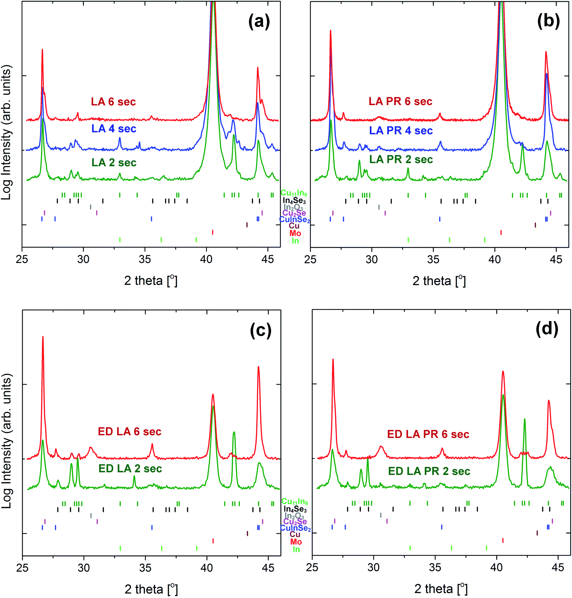 | ||
| Fig. 5 XRD diffractograms for all sample sets: LA vacuum-deposited samples (a), LA pre-alloyed samples (b), LA ED samples (c) and LA pre-alloyed ED samples (d) for each dwell time. | ||
The same patterns are presented in Fig. 6, but for a narrower 2θ range corresponding to the 112 diffraction peak of CuInSe2. For each sample set, the reference sample is included for comparison. The peak gets narrower with the dwell time which indicates a better crystalline quality. To facilitate this observation, the FWHM values and the average apparent crystalline coherence length are plotted with the dwell time (Fig. 7). The crystalline domain size of the samples is increased with the dwell, approaching the values of the reference samples, which are 245 nm for the thick oven and 350 nm for the thick PR oven. Therefore, for the oven-annealed samples, the pre-alloying step increases the crystallinity. This trend is however opposite for the case of the LA samples, with the PR samples having a lower crystalline domain size (250 nm for LA-6 s and 150 nm for LA-PR 6 s, for example). Despite the better phase purity of the pre-alloyed sample set, these samples seem to be composed of smaller grains due to the different morphology of the precursor. This will be further discussed with a proposed growth model in the Discussion section. Finally, the LA samples (even at 6 s dwell times) do not yet exhibit the same narrowing of the peak as the reference sample, and some broadening remains. This may be related with some Cu2−xSe phases still present in the film, which appears as a shoulder in higher 2θ angles. Some broadening may also be related to structural faults or strain within the material20 which may be caused due to the extremely fast heating and cooling rates.
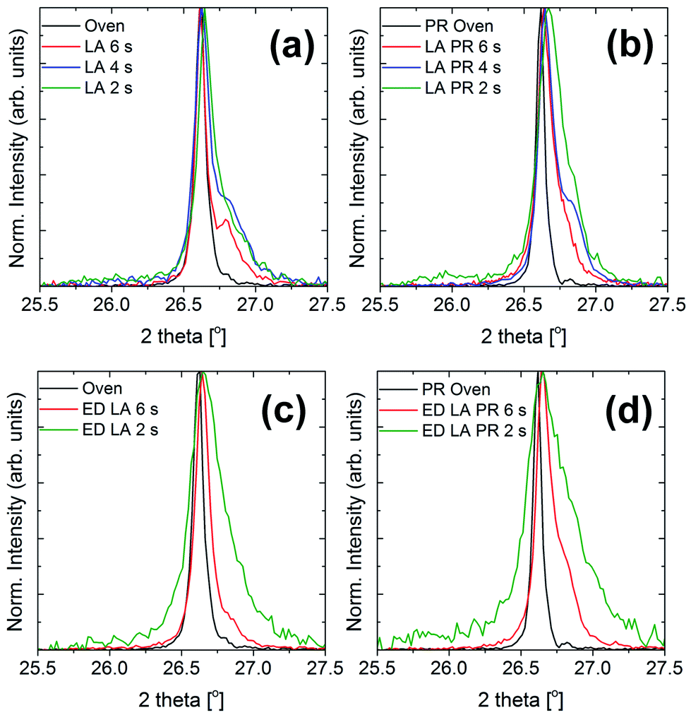 | ||
| Fig. 6 XRD patterns at a narrower 2θ range corresponding to the 112 reflection of CIS for each sample set: LA vacuum-deposited samples (a), LA pre-alloyed samples (b), LA ED samples (c) and LA pre-alloyed ED samples (d). The XRD patterns of the thick oven reference samples are also included for comparison. | ||
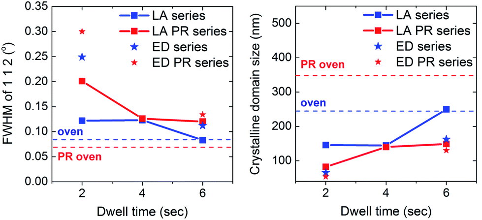 | ||
| Fig. 7 Summary of the FWHM of the CIS 112 peak of all samples and the average crystal coherence length calculated using the Scherrer formula. | ||
Raman spectroscopy was performed to assess the near surface quality of the LA films. Fig. 8 summarises the spectra collected for both sample sets (LA series and LA-PR series) and for each dwell time. All samples exhibit the A1 mode of CuInSe2 phase at ∼175 cm−1. The A1 peak gets narrower with the dwell time, which is also related with better crystalline quality.21 Peak fitting (not shown) shows the presence of an additional peak at 183 cm−1 (position marked by grey dotted line in each spectrum) for the case of 2 and 4 s LA samples. This position is likely assigned to the CuAu (CA) ordered polytype of CuInSe2 which could be associated with insufficient annealing temperatures, as in the case of CuInS2 material.22 The presence of CA ordering has also been observed in CuInSe2 layers grown by molecular beam epitaxy.23 The disappearance of the CA peak with dwell times suggests that a higher temperature is obtained with extended LA time or that sufficient dwell time has been reached to allow the crystals to order into the chalcopyrite structure. With regards to the PR sample set, a new mode at 149 cm−1 is evident for the 2 s sample (also marked by grey dotted line). This peak is related with ordered defect compounds (ODC), commonly found in very Cu-poor samples.24,25 The Raman results are in line with the EDS composition where the 2 s samples exhibited the lowest Cu/In ratio, indicating the highest In composition at the surface. The presence of secondary phases, as suggested by XRD analysis, is not evident by Raman. This can be due to the smaller measurement area (and different probing depth) of Raman analysis compared to XRD.
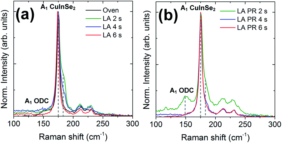 | ||
| Fig. 8 Raman spectra of LA samples (a) and their pre-alloyed counterparts (b). The dotted line at 183 cm−1 is likely assigned to the CuAu polytype phase of CuInSe2. | ||
The degree of the reaction completion can also also be seen with EDS elemental mapping on cross sectional SEM images (Fig. S1, ESI†). Two representative samples were analysed, ED-LA 6 s and ED-PR-LA 6 s. The EDS maps indicate the presence of In-rich secondary phases (InxSey) on the surface of the ED-LA 6 s sample, but in the case of the ED-PR-LA 6 s sample the CIS grains expand throughout the entire film thickness. These results are in line with the XRD analysis, which shows that the reaction is incomplete for the 6 s sample, but the material is phase-pure when the pre-alloying is performed prior to LA.
Finally, the opto-electronic quality of the LA-material was assessed by calibrated PL measurements. The measurements were performed on the LA-PR-6 s sample since XRD shows this to be single phase, as well as on the thick PR oven reference sample, for comparison. Both samples were etched in 10% KCN aqueous solution for 2 minutes, to remove any residual trace oxide phases and/or CuxSe from the surface.26 A thin CdS layer was deposited on the samples prior to the PL measurement, to passivate the absorber layer and to supress its degradation in air.26 Fig. 9 shows that both samples exhibit a single peak emission, at 0.98 eV for the reference material and at 0.93 eV for the LA material. These values are close to the band gap for Cu-poor CuInSe2, expected at 0.96–0.99 eV.27 The LA sample shows a broader PL peak, with the PL maximum red shifted by ∼50 meV, compared to the reference. The red shift suggests that the LA-CIS has a lower Cu/In ratio28,29 compared to the thick reference material with a Cu/In ratio of 0.9. The feature at around 0.9 eV for the reference sample is due to water absorption, which has not been “perfectly” spectrally corrected. The PL peak broadening of the LA sample compared to the reference could be associated with the presence of ODC (seen by Raman for the LA-2 s sample) which are expected to have a higher bandgap than CuInSe2 (ref. 27) and/or the presence of CuAu ordering of CuInSe2 (also seen by Raman).
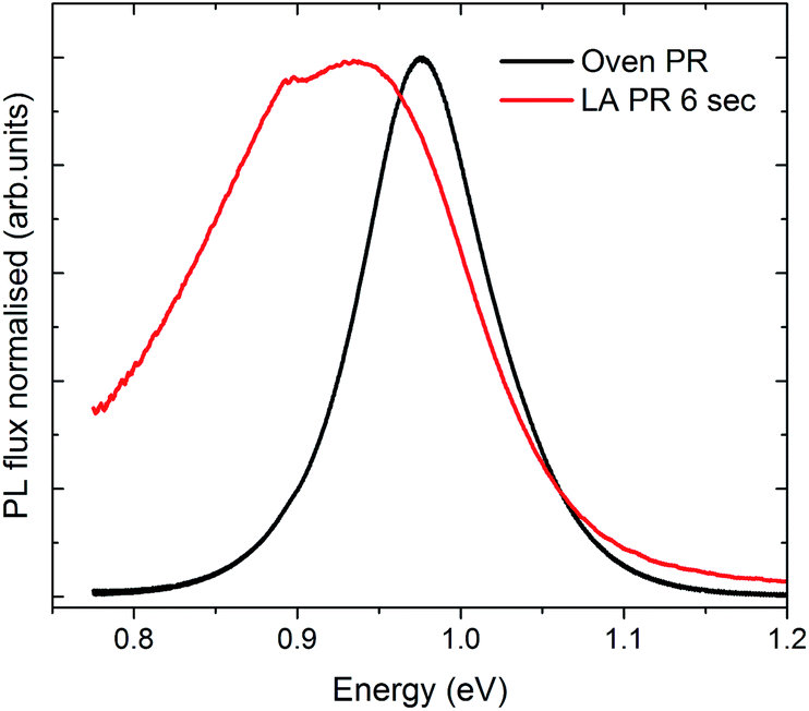 | ||
| Fig. 9 PL spectra of the Oven-PR (thick PR oven) reference sample and LA-PR 6 s sample, measured at equivalent illumination of 11 suns. Both spectra have been normalised to facilitate comparison. | ||
Quasi Fermi level splitting (qFLs) represents an upper limit for the achievable open-circuit voltage (VOC) of a solar cell and thus is a key quality indicator of solar cell device performance.19 The qFLs and the deficit values are summarised in Table 2. The qFLs has been estimated by means of ERE analysis, as described in the Experimental section. The error associated with this value is ∼20 meV due to uncertainty of the band gap estimation and the ERE analysis. The corresponding band gaps EG (needed for VSQOC) were estimated taking into consideration the PL maximum. A qFLs of 425 meV is calculated for the reference sample using two different methods, as described in the Experimental section. The two values match very well, which confirms the credibility of the ERE measurements. As a comparison, the highest observed VOC to date for pure CuInSe2 material is 515 meV.30 For the case of the LA sample, the estimated qFLs value was 320 meV. Nonetheless, if the bandgap is taken into account (lower bandgap value for the LA sample), the difference in the qFLs deficit (EG − qFLs) is only 60 meV. This result implies that the LA material exhibits high optoelectronic quality, similar to the oven-annealed reference.
| Sample | EG (eV) | qFLs at 1 sun (eV) | Deficit EG − qFLs (eV) |
|---|---|---|---|
| Oven PR | 0.978 | 0.425 | 0.55 |
| LA PR 6 s | 0.930 | 0.320 | 0.61 |
Discussion and future directions
Based on the XRD analysis we can deduct qualitative phase information from the samples. The bar chart in Fig. 10 indicates how the intensity of the main diffraction peaks of each phase progresses with the dwell time, for each sample set. Based on this analysis and in combination with the rest of the results, we can elucidate the reaction mechanism for LA of Cu/In stacked precursors.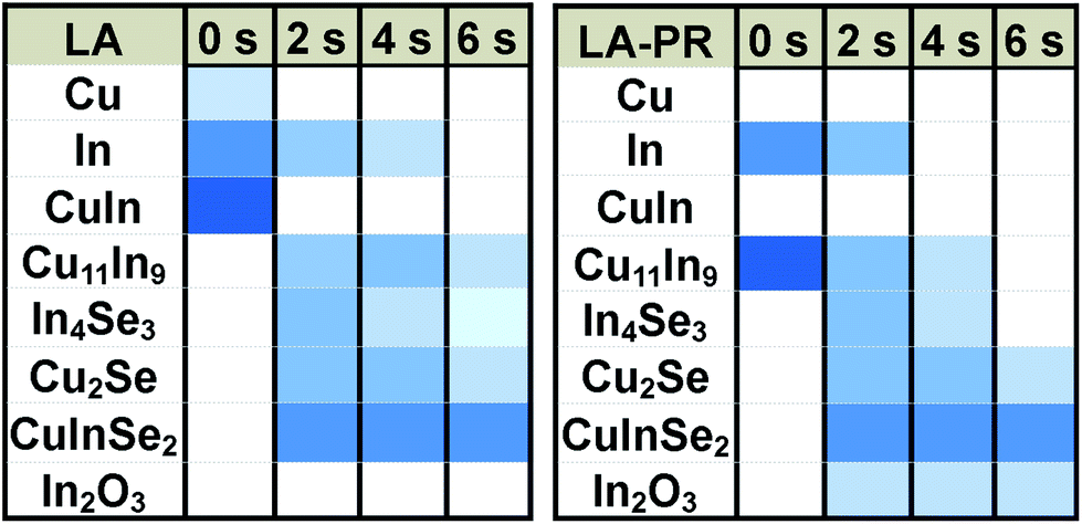 | ||
| Fig. 10 Bar chart representing the relative change in intensity of the main XRD peaks for each phase, as a function of the dwell time. | ||
A proposed reaction path is depicted in Fig. 11. For the non-prealloyed samples, the initial precursor is composed of In islands on top of a Cu compact layer, with some metal intermixing at the interface. This precursor stack only weakly absorbs the 1064 nm radiation,7 and as a result there is a strong elemental gradient remaining in the sample after LA at short dwell times. Based on the EDS and XRD results, CIS already forms after 2 s LA, but the reaction is incomplete. The high In content in these samples implies that there is still a compositional gradient, with In-rich phases present at the surface. In combination with the XRD analysis, this suggests that Cu and In secondary phases are formed, with the InxSey phases likely formed first at the front of the samples. This agrees with the RTP study of Mainz et al.,31 but is opposite to that found by Hergert et al.12 Briefly, Mainz et al. heated CuInGa stacks from room temperature to 600 °C in 90 s with a non-linear temperature ramp and investigated the phase composition with both in situ and ex situ characterisation techniques. At 500 °C, or after 30 s of heating, In–Se phases were observed at the top of the sample. Thereafter at 550 °C, which occurs after 40 s of heating, Cu–Se phases were observed in addition.31 Contrarily, Hergert et al. observed that CuSe2 is formed prior to In4Se3 while heating CuIn metal stacks from room temperature to 425 °C at a rate of 0.44 °C s−1.12 The laser annealing results reported here are consistent with the higher heating rate of Mainz et al.31 suggesting that temperatures of at least 550–600 °C were reached within two seconds.
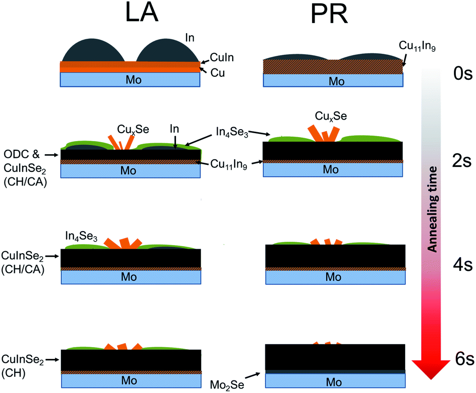 | ||
| Fig. 11 Proposed reaction path for LA of Cu/In precursors, for non-pre-alloyed samples (LA) and pre-alloyed samples (PR). | ||
With increasing dwell times, the binary phases react with each other, forming CIS at the interface of In metal and Cu11In9 alloy. The CIS layer further grows with annealing time, while the secondary phases are being consumed. EDS analysis also shows volume expansion with the dwell time, with the LA-6 s sample approaching the thickness of the reference material. The oven annealed sample with a heating time of 90 min is fully recrystallised and it is expected to have no metal composition gradient. The similar sample thickness (comparable Mo signal) and Cu/In ratio between the LA 6 s sample and the reference sample suggest that the LA material approaches reaction completion. In comparison, for the RTP of Mainz et al.,31 CuInSe2 was first observed at 560 °C, achieved after 55 s of heating, and the full metal stack was fully converted into the ternary semiconductor after 90 s where the temperature reached 600 °C. In other words, 45 s were required to go from the first observation of CuInSe2 to the complete layer conversion.31 Having said this, based on the XRD analysis of the LA-6 s sample, a small amount of secondary phases remain, as well as some unreacted precursor in the form of the Cu11In9 alloy. The incomplete reaction and the strong elemental gradient in LA films have also been observed in RTP-annealed metallic precursors with stoichiometric Se amount.12 At the same time, when Se was supplied in excess (10 times more), the secondary phases were not observed.12 This could suggest that the strong elemental gradient in LA material is related to an insufficient Se partial pressure.
With regards to the CIS phase, its composition and structure also change with the dwell time. Specifically, the Cu content increases with the dwell time. At short annealing times the CIS phase (at least to some extent) is in the form of ODCs, as seen by Raman. Longer annealing times promote the Cu inclusion in the structure, such that the CIS composition approaches the composition of the reference material, but the material remains Cu-poor. The Cu-poor composition of CIS can also be observed by PL, with the PL peak being red shifted compared to the bandgap of pure CIS.28,29 Apart from the composition, there is evidence for a change of the cation ordering in CIS, with short annealing times favouring the CA polytype phase. Based on Raman analysis, the CA polytype phase is progressively disappearing with annealing time, and the chalcopyrite (CH) phase becomes the dominant structure. Further investigation in the cation ordering of the CIS phase and distinction between CA/CH structures is required, which will be done in future work.
A further consequence of the changing sample composition with time is the difficulty to model its temperature time profile, since all the optical and thermal properties depend heavily on the chemical composition. As discussed above, the metal stacked precursors of Mainz et al. required 45 s at temperatures above 560 °C to ensure that the whole of the layer consisted of ternary semiconductors.31 This suggests that the laser annealed sample must have been at least at this temperature, if not higher. Previous attempts to model such profiles assumed the presence of unchanging phases.7 Essentially once either binary or ternary selenides have formed, under 1064 nm irradiation with a power of 150 W cm−2 it was found that the samples reached a temperature of 650 °C after 1 s, and the profile of the heating curve suggested that a steady state temperature of 700 °C would be reached after 1.5 s. Given that the analysis of the LA 2 s sample clearly shows the presence of binary and ternary compounds, it is likely that the sample then reaches a maximum temperature of 700 °C after 3.5 s annealing.
For the pre-alloyed precursor material, all the Cu is alloyed with In to form the Cu11In9 alloy, with excess In remaining on the surface. In islands are flatter and more spread out in comparison to the non-pre-alloyed sample. It should be noted that the Cu11In9 alloy is present in both sample sets, however, it forms at an earlier stage in the pre-alloyed samples. This fact causes two separate effects. First, the reaction rate for CIS formation is enhanced, due to better metal intermixing prior to LA. This was illustrated with several methods: EDS analysis shows a slightly higher Cu and Se content, which confirms a better intermixing. XRD analysis shows the disappearance of In4Se3 and Cu11In9 peaks for the LA-PR-6 s sample, whilst these phases are still present in the LA-6 s sample. Similarly, EDS mapping on the cross sectional images (Fig. S2, ESI†) shows the same effect, with the ED-PR-6 s approaching reaction completion, whilst the ED-6 s counterpart sample containing In-rich phases towards the front. Overall, the pre-alloying step enhances the reaction rate and can result in phase-pure material for 6 s annealing time.
Separately, pre-alloying seems to influence the grain morphology, resulting in a smaller CIS grain size upon LA. This is likely related to the morphology of the pre-alloyed precursor film. The spreading of the In islands (Fig. 1) increases the contact area with the underlying precursor layer. This causes a higher density of nucleation sites and as a result, grains are smaller but more densely packed32 than the non-pre-alloyed sample. The difference in the grain size between the two sample sets can be observed from the crystalline domain size (Fig. 7).
In conclusion, a 6 s annealing time seems to be sufficient for a complete reaction, provided that the metal precursor is alloyed prior to LA. We have shown that samples processed in these conditions approach phase-purity, with crystalline quality similar to the reference material annealed at equilibrium conditions. The crystalline quality is indicated by the narrowing of the main CIS chalcopyrite peaks in XRD and the A1 CIS vibrational mode in Raman, where the peaks approach the FWHM values of the reference sample. Finally, the qFLs deficit (EG − qFLs) obtained by PL analysis of the LA-PR-6 s sample is only 60 meV lower than the reference, which confirms the high opto-electronic quality of LA-CIS.
Based on peak broadening in Raman and PL peaks, structural defects may be present in the LA material. The nature of these structural defects and their effect on device performance remains unclear. Key to future improvement will be the elimination of these defects. Further, the precursor morphology and intermixing should be further investigated, as it appears to be very critical for this application. An ideal precursor configuration should have a continuous coating of In on top of Cu, rather than In islands, so that the contact area between the metal layers is bigger. In this way, the Cu will not remain exposed to Se vapour during LA, CuxSe phases will form at a later stage and will not limit the reaction rate for CIS formation. A precursor with intimately mixed metals, as in the case of co-sputtered Cu/In precursor,11 is expected to exhibit higher reaction rates.
In terms of precursor composition, the targeted Cu/In ratio in this work was 0.8–0.9. Since some of the Cu remains at the back of the sample after LA, the overlying CIS appears to be even more Cu-poor. To mitigate this effect, the precursors should be made more Cu-rich, which will further improve the crystallinity and opto-electronic properties of the absorber. Also, the targeted absorber thickness was 0.5 μm, which appears to be the optimum thickness for the LA parameters used. Slightly thicker samples, as in the case of ED samples, appear to still have some unreacted Cu11In9 alloy at the back (Fig. 5, sample ED-PR-LA 6 s). This suggests that for absorbers in the range of 1 μm thickness, which would be optimum for photon absorption,33 the LA conditions would have to be adjusted accordingly.
Experimental section
Two separate precursor types were used for this study. Most of the analysis was performed on vacuum-deposited layers, comprised of sputtered Cu and thermally evaporated In. Vacuum-deposited samples were primarily used for LA to facilitate the characterisation, as they are more uniform over the sample area compared to electro-deposited precursors. The thicknesses of Mo/Cu/In layers were 750, 90 and 225 nm, respectively. These samples are denoted as “thin”. The same type of sample, but with Cu and In layer thicknesses of 155 and 385 nm instead, are denoted as “thick”. One of each precursors (thin and thick) were annealed in a tube furnace to be used as reference samples, whilst LA is only performed on thin samples. The precursors were prepared targeting a Cu/In ratio of 0.8–0.9 and a final absorber thickness of 0.5 and 1 μm after selenisation, for the thin and thick precursors respectively.The second group of precursors was prepared by electrodeposition of Cu using an alkaline aqueous bath,34 followed by In electrodeposited in an ionic liquid.16 Both sets of precursors were prepared on a molybdenum-coated soda-lime glass substrate of 2 mm thickness. The electro-deposited precursors were deposited targeting similar Cu/In thicknesses (and eventually composition) as the thin vacuum precursors and were controlled by tuning the total charge passed during each deposition. These samples will be denoted as “thin-ED”. Finally, excess Se was deposited onto the Cu/In layers by thermal evaporation. During Se evaporation, the sample temperature was set to room temperature, to avoid any reactions between the metals and Se vapour. The real temperature during evaporation was monitored with a thermocouple located at the back of the substrates, which did not exceed 21 °C during deposition. The final Se thickness was ∼800 nm.
LA was performed using a CW Nd:YAG solid state laser, which emits a wavelength of 1064 nm. A 2 × 2 mm aperture was placed in the laser path, and a laser flux 150 W cm2 was kept constant and measured after the aperture. The sample was placed inside a sealed chamber with a transparent heated window and the chamber was purged with nitrogen gas prior to LA. The window is heated to 150 °C in order to maintain a partial pressure of selenium above the sample during LA, which was found to be critical for good re-crystallisation of mixed elemental precursors.7 The chamber was mounted on a controlled x-y stage to raster the laser beam across the sample. The laser rastering is illustrated in the schematic of Fig. S2 (ESI†). The beam was scanned horizontally from one side to the other, and then vertically translated by 1.5 mm, before being horizontally scanned again in the opposite direction. The horizontal lines scanned by the laser are partially overlapping to eliminate material non-uniformities that may be caused by the Gaussian laser beam intensity profile. Samples will be named based on the heating dwell time, which is the amount of time a single spot is heated, therefore dividing the beam size with the scan rate. The annealing dwell time is varied from 2 to 6 s, which corresponds to scan rates of 1 to 0.33 mm s−1. All samples were etched after LA in Na2S 0.5 M aqueous solution to remove any unreacted Se on the surface and to facilitate characterisation.
Two separate samples were annealed in a tube furnace as the reference samples and they are denoted as “thin or thick oven”. The sample was placed inside a graphite box with Se powder and the annealing was performed in a closed reactor with a starting pressure of 30 mbar. A three step annealing recipe was used, at 100, 400 and 580 °C, and for 30, 15 and 30 min dwell time in each step, respectively. Including the heating rate of the oven (∼45 °C min−1), the total heating time for this sample exceeds 90 min. A three stage annealing step has been shown to improve crystallisation, grain growth and selenium incorporation in the absorber film.35,36
A mild heating step was implemented for a group of precursor samples to promote the alloying between Cu and In layers, prior to LA. Each pre-alloyed sample set will be denoted with the prefix “PR”. The pre-alloying step was performed for the Cu/In precursors (prior to the deposition of the Se “capping” layer) on a hot plate at ∼200 °C inside a nitrogen-filled glove box.
Scanning electron microscopy (SEM) and energy dispersive X-ray spectroscopy (EDX) analysis were performed using a Hitachi SU 70 electrical microscope. X-ray diffraction (XRD) measurements were made using a Bruker system with Cu Kα radiation and in θ–2θ Bragg–Brentano geometry. The XRD measurements were performed near the centre of each LA area, with a fixed incident beam width of 3 mm. The apparent crystalline coherence length has been calculated based with the FWHM values, using the Scherrer formula, with the Scherrer constant (K) of 1.37 The instrumental response function is measured using an Al2O3 standard. Raman measurements were performed with a Renishaw inVia micro-Raman spectrometer, using a 532 nm laser excitation at a power of 0.2 mW and a laser beam spot size of 0.9 μm. Finally, calibrated photoluminescence (PL) measurements have been performed using a 663 nm diode laser as the excitation source. For photon counting and for quasi Fermi level splitting (qFLs) evaluation, two corrections are applied to the raw data. The spectral correction is performed using a reference white light lamp with a known spectrum. For the intensity correction, the laser power and the beam diameter were measured with a power meter and a CCD-camera, respectively. In this way, the incident photon flux is estimated and was related to the photon flux of the AM 1.5 sun spectrum above the CIS absorber layer sample bandgap. The qFLs has been estimated by means of the external radiative efficiency (ERE) analysis, considering that:
VSQOC − qFLs = kT![[thin space (1/6-em)]](https://www.rsc.org/images/entities/char_2009.gif) lnERE lnERE |
Conclusions
Metal stacked layers were laser annealed to form CIS thin films with annealing times of up to 6 s, a much shorter timescale compared to conventional annealing routes. The reaction mechanism was presented by analysing ex situ X-ray diffractograms, Raman spectra and composition data. We show that the CIS formation occurs via the formation of CuxSe/InxSey binary phases, as in the case of oven annealing. For the first time, a pre-alloying step is applied on precursors for laser annealing, and it was shown to drastically promote elemental intermixing and to enhance the reaction rate. Laser annealing for six seconds approaches near phase-pure material which exhibits similar crystalline quality and opto-electronic properties as the reference material annealed in a tube furnace. The estimated qFLs deficit for this material is only 60 meV lower than the reference sample, which highlights the potential of LA CIS for solar cell processing. Some structural defects may be present in the material which will be eliminated in future work.Conflicts of interest
There are no conflicts to declare.Acknowledgements
This work was supported by Fonds National de la Recherche du Luxembourg and the IRP LASER2 project. P. A. would like to thank Dr Michele Melchiorre from the University of Luxembourg for assistance with SEM imaging and Sudhajit Misra from the University of Utah for assistance with the laser maintenance.References
- B. J. Simonds, H. J. Meadows, S. Misra, C. Ferekides, P. J. Dale and M. A. Scarpulla, J. Photonics Energy, 2015, 5, 050999 CrossRef.
- F. Kessler, D. Herrmann and M. Powalla, Thin Solid Films, 2005, 480, 491–498 CrossRef.
- P. Magazine, Solar Frontier hits new CIS cell efficiency record, https://www.pv-magazine.com/2019/01/21/solar-frontier-hits-new-cis-cell-efficiency-record/ Search PubMed.
- T. Kato, J. L. Wu, Y. Hirai, H. Sugimoto and V. Bermudez, IEEE Journal of Photovoltaics, 2019, 9, 325–330 Search PubMed.
- K. Kushiya, A. Shimizu, K. Saito, A. Yamada and M. Konagai, in Proceedings of 1994 IEEE 1st World Conference on Photovoltaic Energy Conversion – WCPEC, 2002, pp. 87–90 Search PubMed.
- K. Kim, G. M. Hanket, T. Huynh and W. N. Shafarman, J. Appl. Phys., 2012, 111, 083710 CrossRef.
- H. J. Meadows, S. Misra, B. J. Simonds, M. Kurihara, T. Schuler, V. Reis-Adonis, A. Bhatia, M. A. Scarpulla and P. J. Dale, J. Mater. Chem. C, 2017, 5, 1336–1345 RSC.
- H. Deligianni, L. T. Romankiw, D. Lincot and P.-P. Grand, in Electrochemical Engineering, 2018 Search PubMed.
- L. D. Laude, M. C. Joliet and C. Antoniadis, Sol. Cells, 1986, 16, 199–209 CrossRef CAS.
- D. Bhattacharyya, S. Bocking and M. J. Carter, J. Mater. Sci., 1996, 31, 5451–5456 CrossRef CAS.
- F. O. Adurodija, J. Song, S. D. Kim, S. H. Kwon, S. K. Kim, K. H. Yoon and B. T. Ahn, Thin Solid Films, 1999, 338, 13–19 CrossRef CAS.
- F. Hergert, R. Hock, A. Weber, M. Purwins, J. Palm and V. Probst, J. Phys. Chem. Solids, 2005, 66, 1903–1907 CrossRef CAS.
- Q. Zhang, H. Deng, J. Yu, J. Tao, L. Sun, P. Yang and J. Chu, Mater. Sci. Eng., B, 2019, 242, 31–36 CrossRef CAS.
- F. O. Adurodija, M. J. Carter and R. Hill, Sol. Energy Mater. Sol. Cells, 1995, 37, 203–216 CrossRef CAS.
- J. S. Chen, E. Kolawa, M.-A. Nicolet and R. P. Ruiz, Sol. Cells, 1991, 30, 451–458 CrossRef CAS.
- J. C. Malaquias, M. Steichen, M. Thomassey and P. J. Dale, Electrochim. Acta, 2013, 103, 15–22 CrossRef CAS.
- Z. Bahari, E. Dichi, B. Legendre and J. Dugué, Thermochim. Acta, 2003, 401, 131–138 CrossRef CAS.
- L.-C. Yang, C. Y. Cheng and J. S. Fang, J. Phys. Chem. Solids, 2008, 69, 435–440 CrossRef CAS.
- U. Rau, D. Abou-Ras and T. Kirchartz, Advanced characterization techniques for thin film solar cells, John Wiley & Sons, 2011 Search PubMed.
- T. Ungár, Scr. Mater., 2004, 51, 777–781 CrossRef.
- R. Scheer, A. Pérez-Rodríguez and W. K. Metzger, Prog. Photovolt. Res. Appl., 2010, 18, 467–480 CrossRef CAS.
- J. Álvarez-García, A. Pérez-Rodríguez, A. Romano-Rodríguez, J. R. Morante, L. Calvo-Barrio, R. Scheer and R. Klenk, J. Vac. Sci. Technol. A, 2001, 19, 232–239 CrossRef.
- J. Álvarez-García, B. Barcones, A. Pérez-Rodríguez, A. Romano-Rodríguez, J. R. Morante, A. Janotti, S.-H. Wei and R. Scheer, Phys. Rev. B: Condens. Matter Mater. Phys., 2005, 71, 54303 CrossRef.
- W. Witte, R. Kniese and M. Powalla, Thin Solid Films, 2008, 517, 867–869 CrossRef CAS.
- B. J. Stanbery, Crit. Rev. Solid State Mater. Sci., 2002, 27, 73–117 CrossRef CAS.
- D. Regesch, L. Gütay, J. K. Larsen, V. Deprédurand, D. Tanaka, Y. Aida and S. Siebentritt, Appl. Phys. Lett., 2012, 101, 112108 CrossRef.
- L. Gütay, D. Regesch, J. K. Larsen, Y. Aida, V. Depredurand, A. Redinger, S. Caneva, S. Schorr, C. Stephan, J. Vidal, S. Botti and S. Siebentritt, Phys. Rev. B Condens. Matter Mater. Phys., 2012, 86, 045216 CrossRef.
- S. Siebentritt, L. Gütay, D. Regesch, Y. Aida and V. Deprédurand, Sol. Energy Mater. Sol. Cells, 2013, 119, 18–25 CrossRef CAS.
- I. Dirnstorfer, M. Wagner, D. M. Hofmann, M. D. Lampert, F. Karg and B. K. Meyer, Phys. Status Solidi, 1998, 168, 163–175 CrossRef CAS.
- T. Unold and H. W. Schock, Annu. Rev. Mater. Res., 2011, 41, 297–321 CrossRef CAS.
- R. Mainz, A. Weber, H. Rodriguez-Alvarez, S. Levcenko, M. Klaus, P. Pistor, R. Klenk and H. W. Schock, Prog. Photovolt. Res. Appl., 2015, 23, 1131–1143 CrossRef CAS.
- M. Easton and D. St John, Metall. Mater. Trans. A, 2005, 36, 1911–1920 CrossRef.
- S. S. Hegedus and W. N. Shafarman, Prog. Photovolt. Res. Appl., 2004, 12, 155–176 CrossRef CAS.
- J. J. Scragg, D. M. Berg and P. J. Dale, J. Electroanal. Chem., 2010, 646, 52–59 CrossRef CAS.
- S. G. Haass, M. Diethelm, M. Werner, B. Bissig, Y. E. Romanyuk and A. N. Tiwari, Adv. Energy Mater., 2015, 5, 1500712 CrossRef.
- E. Lee, S. J. Park, J. W. Cho, J. Gwak, M.-K. Oh and B. K. Min, Sol. Energy Mater. Sol. Cells, 2011, 95, 2928–2932 CrossRef CAS.
- D. M. Smilgies, J. Appl. Crystallogr., 2009, 42, 1030–1034 CrossRef CAS.
- P. Wurfel, J. Phys. C: Solid State Phys., 1982, 15, 3967–3985 CrossRef.
Footnote |
| † Electronic supplementary information (ESI) available: Compositional mapping on cross section images, digital photograph of a laser-annealed sample, description of laser scan movement. See DOI: 10.1039/c9ra06896a |
| This journal is © The Royal Society of Chemistry 2020 |