
 Open Access Article
 This Open Access Article is licensed under a Creative Commons Attribution-Non Commercial 3.0 Unported Licence
Electronic and transport properties of zigzag phosphorene nanoribbons with nonmetallic atom terminations
L. Sunabc,
Z. H. Zhang b,
H. Wang*c and
M. Li*ad
b,
H. Wang*c and
M. Li*ad
aSchool of Physics and Electronics, Central South University, Changsha 410083, China
bSchool of Physics and Electronic Science, Changsha University of Science and Technology, Changsha 410114, China
cGuangdong Provincial Key Laboratory of Micro/Nano Optomechatronics Engineering, College of Mechatronics and Control Engineering, Shenzhen University, Shenzhen 518060, China. E-mail: whao@szu.edu.cn; Fax: +86 755 26557471; Tel: +86 755 22673522
dSchool of Materials Science and Engineering, Georgia Institute of Technology, Atlanta, Georgia 30332, USA. E-mail: mo.li@gatech.edu; Tel: +1 404 385 2472
First published on 8th January 2020
Abstract
Using the first-principles method based on density-functional theory and nonequilibrium Green's function, electronic properties of zigzag phosphorene nanoribbons (ZPNRs) terminated with nonmetallic (NM) atoms such as H, C, F, N, O, S and Si, as well as a pristine case, are studied systematically. Three possible cases are considered, namely, ZPNRs with symmetrical edge terminations, asymmetrical edge terminations, and the half-bare edge case. It is shown that the pristine ZPNRs show metallic behavior. For ZPNRs terminated with C, O, S and Si atoms, they are always metals regardless of the termination cases. For ZPNR terminated with H, F, and N, the electronic structure is either a metal or a semiconductor, which depends on the termination cases. The results from the calculated edge formation energy show that the ribbons with C, F, N, O, S and Si atom edge modifications are more stable than the H-terminated ZPNR. Moreover, an applied external transverse electric field can effectively modulate the bandgaps of ZPNRs terminated with H, F and N, especially reducing the gap with the increase of the applied external transverse electric field strength. The ZPNRs terminated with N undergo a semiconductor-to-metal transition. We also investigate the electronic transport properties in nano devices consisting of the ZPNRs terminated respectively by O and S at both edges and with the fully bare edge. It is found that O and S terminated ZPNR devices have a good linear response on bias, and the current is bigger than the pristine case. The results indicate that the introduction of NM atoms at the edge(s) can effectively modulate the electronic and transport properties of ZPNRs. These novel electronic properties suggest that PNRs are a promising candidate for future nanoelectronic and optoelectronic applications.
1. Introduction
Phosphorene or monolayer black phosphorus has been fabricated recently by using the same mechanical exfoliation methods as for graphene. The new two dimensional material has not only attracted a great deal of interests from the fields of electronic engineering and materials science, it has also drawn significant attentions for device applications such as solar cells, batteries, supercapacitors and many others.1–12 In bulk form, black phosphorus consists of puckered honeycomb layers of phosphorus atoms which are held together via van der Waals interactions. Phosphorene has many superior properties such as a carrier mobility up to 1000 cm2 V−1 s−1 and an on/off ratio up to 105 achieved in the phosphorene transistors at room temperature.1 In addition, this material has a finite direct bandgap ranging from about 1.5 eV for a monolayer13,14 to 0.3 eV for multilayers,15,16 which is striking in contrast to zero-gap graphene. This basic and important property is fundamental to building switchs in transistor devices.To explore potential applications of phosphorene in micro- and nano-electronics, the electronic properties have been tuned by several methods. Hashmi et al.17 demonstrate that the spin polarized semiconducting state can be realized in phosphorene by substitutional doping of Ti, Cr, and Mn, while a half-metallic state is obtained by V and Fe doping. Hu et al.18 obtained the spin polarized band structures in Fe, Co and Au doped phosphorene with a band gap, and a Cr doped phosphorene displays a magnetic state.
As for phosphorene nanoribbons (PNRs), their electronic properties are dependent on the crystal orientation of the ribbons. Tailoring the phosphorene along with different directions, two typical families of PNRs can be obtained, the armchair-edge (APNRs) and zigzag-edge PNRs (ZPNRs). Wu et al.1 found that the band gaps of both APNRs and ZPNRs decrease monotonously with increasing ribbon width and eventually converge to the band gap of 2D phosphorene. Guo et al.19 found that the pristine ZPNRs are metals regardless of the ribbon width, while the pristine APNRs are semiconductors. Tran & Yang20 reported that the PNRs with the edge P atoms passivated by H atoms are direct-gap semiconductors and their band gaps are a strong function of the ribbon width due to quantum confinement effect when the band width is between 5 to 12. Peng et al.21 studied the edge effects on the electronic properties of the PNRs with the edge functionalized with different chemical groups. They reported that the APNRs are semiconductors for all edge groups, and the ZPNRs demonstrate either semiconducting or metallic behaviors depending on different edge passivation. Li et al.22 reported that through edge hydrogenation, both the armchair and zigzag PNRs become semiconductors with a direct band gap, and the structure becomes more stable.
These results imply that it is of importance to systematically study the edge effects on the PNRs. This paper selects the ZPNRs with the edge effect as the research topic. The ZPNRs are terminated with nonmetallic (NM) atoms in multiple terminations. Our results suggest that the ribbons with C, F, N, O, S and Si atom edge modifications are more stable than the H-terminated ones. In addition, we found that the introduction of the nonmetallic elements and the applied external transverse electric field can effectively modulate the electronic properties of ZPNRs, making them going through a semiconductor-to-metal transition. Furthermore, O and S modified ZPNRs device have a good linear response on bias, and the current is bigger than the pristine case. These novel electronic properties suggest that PNRs is a promising candidate for the future nanoelectronic and optoelectronic applications.
2. Structure model and theoretical methods
Fig. 1 shows a ZPNRs superlattice model which is infinite along the ribbon direction with the edge terminations on the other direction. Here the ribbon width (“W”) represents the number of phosphorus atom chains along the ribbon width direction. Here we consider the ZPNRs with width W = 6. Among the nonmetallic edge atoms, blue and red balls indicate X and Y atoms, respectively, namely X, Y![[double bond, length as m-dash]](https://www.rsc.org/images/entities/char_e001.gif) H, F, C, N, O, S and Si.
H, F, C, N, O, S and Si.
 | ||
| Fig. 1 The geometrical structures of the nonmetallic atom terminated ZPNRs, denoted as X-ZPNR-Y (X, YH, F, C, N, O, S, and Si). The black dotted rectangle exhibits a minimum repeated unit (supercell) used in this work. | ||
Three different kinds of NM atom terminations are considered: (1) symmetrical edge terminations, that is, both edges of ZPNRs are terminated with the same NM atoms, marked as X-ZPNR-X or Y-ZPNR-Y, (2) asymmetrical edge terminations where H atoms are fixed to passivate one edge and other NM atoms terminate the other edge, which is denoted as X-ZPNR-H(YH), and (3) the half-bare edge case where only one edge is terminated with NM atoms while the other edge is bare, referred to as X-ZPNR (without Y). The black dotted box in Fig. 1 exhibits a minimum repeated unit (supercell) used for the calculations of the electronic structures.
The geometry optimizations and the calculations of electronic properties are performed by first-principles method based on the density functional theory (DFT) combined with the non-equilibrium Green's function (NEGF) technique. All calculations are implemented in Atomistix ToolKit (ATK).23–27 The local density approximation (GGA) is used as the exchange correlation function in solving the Kohn–Sham equation. The Troullier–Martins normconserving pseudopotentials is used to represent the atom core and linear combinations of atomic orbitals to expand the valence states of electrons. The k-point sampling is chosen as 1 × 1 × 100 in the Brillouin zone, and 150 Ry is set as the cutoff energy for the grid integration to mainly control the size of the real space integral network partitioning and the solution of the Poisson equation. Full optimization of the atomic structures including the atomic positions and lattice parameters has been carried out with Quasi Newton method under the periodic boundary condition. All calculations are performed after the geometry is optimized until all residual forces on each atom are smaller than 0.02 eV Å−1. The relaxed lattice constants for monolayer phosphorene are a = 3.262 Å and b = 4.476 Å. The results are in good agreement with the experimental values28 and other theoretical calculations.13 To simulate a ribbon, a unit cell with periodic boundary condition is used. Vacuum layers of 15 Å both in plane and out of plane of the ribbons are used to avoid the interaction between periodic images.
3. Results and discussions
3.1 ZPNRs with symmetrical edge terminations
Fig. 2 displays the electronic properties of X-ZPNR-X, including the band structure (BS) (left panel), the total density of states (DOS, marked as Total) and atom-projected density of states (PDOS) (two right panels). The PDOS is the DOS projected on the edge atom and termination atom X. It reflects the contribution of featured atoms to the total DOS. For the purpose of comparison, we first present the electronic properties for the fully bare-edge ZPNR in Fig. 2(a). Clearly, it shows a metallic behavior. Particularly, from the PDOS, we can see the contribution of edge P atoms to the electronic structure of the bare-edge ZPNR. A large PDOS peak related to edge P atoms occurs at the Fermi level. This means that the metallic behavior of the bare-edge ZPNR originates from the edge states. To demonstrate intuitively the effect of the edge states, the Bloch state is calculated, as an example, with the k point selected at the intersection site of a certain subband and the Fermi level marked by the red circle in Fig. 2. We can see that the wave function, shown as the inset in the left panel of Fig. 2(a), is localized at the edges of the ribbon and forms the localized edge state. | ||
| Fig. 2 The band structure (BS), the total density of states (DOS), atom-projected density of states (PDOS), and the Bloch state of X-ZPNR-X for (a) the fully bare-edge ZPNR, (b) H-ZPNR-H, (c) F-ZPNR-F, (d) C-ZPNR-C, (e) N-ZPNR-N, (f) O-ZPNR-O, (g) S-ZPNR-S, and (h) Si-ZPNR-Si. | ||
The electronic properties of the X-ZPNR-X are shown in Fig. 2(b)–(f), respectively. We can see that the introduction of the NM atoms can effectively modulate the electronic structure of the ribbon. The electronic structure of both H-ZPNR-H and F-ZPNR-F exhibit semiconducting characteristics with a direct band gap located at the Γ point in the reciprocal space, as manifested in Fig. 2(b) and (c), but the situation is more outstanding. For the H-ZPNR-H, the bandgap is much bigger than that of the F-ZPNR-F. The calculated PDOS shows that H atoms have little presence to the lowest conduction band (LCB) and the highest valence band (HVB), respectively. The Bloch states for the conduction band minimum (CBM) and valence band maximum (VBM) present these features more prominently. The wave function decays on two edges in CBM and VBM states; and there is little presence of the wave function distribution at the edge atoms and most of the states concentrate in local area around the center inside the ribbon. Both VBM and CBM are contributed by hybridized s–p states of the P atoms in the central region of the nanoribbons. As a matter of fact, the H–P bond is stronger than the P–P bond such that the edge states of PNRs are located deep in the bands. For the F-ZPNR-F, F atoms have a significant contribution to the CBM and VBM. Both structures have the similar electronic property because each F atom has seven electrons in the outer shell and can form a stable structure just by one covalent bond with edge P atoms, which is similar to the case of H atom, but the higher electronegativity of F atom makes such a bond mainly ionic that can be treated as covalent polar, which is different from the H-termination. This difference leads to the different electronic structures between H-ZPNR-H and F-ZPNR-F. For the N-ZPNR-N, the ZPNRs exhibit semiconducting property with an indirect band gap. The CBM and VBM concentrate in the local area at two edges, and there is little presence of the wave function distribution in the local area around the center inside the ribbon.
The above results show that the large band gap can be expected to be obtained by termination with NM atoms such as H, F, N. This has a significance for developing PNRs-based field effect transistors (FETs). In addition, we show that the edge saturation by nonmetallic element H, F and N can make ZPNRs open a big energy gap. This property allows the nanoribbon to be developed into devices based on black phosphorus field effect tube – the “off” state can effectively block the leakage current.
Contrary strikingly to H-ZPNR-H, F-ZPNR-F and N-ZPNR-N, ZPNRs terminated with C, O, S, and Si atoms exhibit metallic behaviors. Clearly, two new subbands passing through the Fermi level are introduced, and from the PDOS and the Bloch states, we can identify that they originate primarily from the termination atoms C, O, S, and Si. Namely, the edge states created from the termination atoms are just located around the Fermi level. This is easily understood because after forming covalent bonds C, O, S, and Si to edge P atom, these termination atoms still have a few unpaired electrons and the corresponding states just reside near the Fermi level. This implies that ZPNRs are sensitive to the edge modifications and the termination atoms can determinate their electronic structures predominately. Furthermore, we can see that the PDOS peaks of termination atoms (C, O, S, and Si) and edge P atom line up to each other, which indicates that a strong coupling and hybridization occur between them. But unlike the pristine ZPNRs, as can be seen from the PDOS and the Bloch states, C, O, S and Si atoms have made significant contributions to the near Fermi level state, while the atoms in the nanoribbon have no contribution at all.
Structural stability is of great significance to experimental synthesis and practical applications. To find the stability for X-ZPNR-X, we calculate their edge formation energy, which is defined as Eedge = (Eribbon-X − Eribbon − nXEX)/2L, where Eribbon-X is the total energy of the ZPNRs terminated with the NM atoms, Eribbon is the total energy of the pristine ZPNRs, EX is the energy of an isolated atom X (C, F, H, N, O, S and Si), all units are in eV, nX is the number of the X atom in a unit cell, and L is the length of the unit cell in the horizontal direction. The unit is nm. The results show that edge formation energies for structures H-ZPNR-H, C-ZPNR-C, F-ZPNR-F, N-ZPNR-N, O-ZPNR-O, S-ZPNR-S and Si-ZPNR-Si are −12.77, −15.90, −16.65, −20.27, −21.39, −15.17 and −15.57 eV nm−1, respectively. As we know, the negative value for the edge formation energy means that this structure is formed by an exothermal process, and the lower edge formation energy suggests a more stable structure. Therefore, we can conclude that all structures are stable. This suggests that these ribbons might be fabricated in the experiment. Particularly, we would mention that compared with H-ZPNR-H, the stability of the ribbons terminated with other NM atoms is enhanced.
3.2 ZPNRs with asymmetrical edge terminations
The electronic properties of the ZPNRs whose one edge is fixed to be passivated with H atoms and another edge is terminated with other NM atoms (C, F, N, O, S and Si) are shown in Fig. 3(a)–(f). The ZPNR structure is asymmetric in the transverse direction, represented as X-ZPNR-H. It can be seen that the termination of F and N is similar to that of symmetric termination on both sides. The F-ZPNR-H is semiconductor with a direct band gap in which both the VBM and CBM are located at the Γ point. N-ZPNR-H is a semiconductor with an indirect band gap. The CBM is located at the Z point and the VBM is located at the Γ point, which all come from the contribution of the edge P atoms and the termination atoms. | ||
| Fig. 3 The band structure (BS), the total density of states (DOS) and atom-projected density of states (PDOS), and the Bloch state of X-ZPNR-H for (a) C-ZPNR-H, (b) F-ZPNR-H, (c) N-ZPNR-H, (d) O-ZPNR-H, (e) S-ZPNR-H, and (f) Si-ZPNR-H. | ||
C-ZPNR-H, O-ZPNR-H, S-ZPNR-H and Si-ZPNR-H also demonstrate metallic behaviors. The interesting aspect here is that the number of the subband across the Fermi level is just reduced by half, from 2 to 1, as compared with the band structure in the case of X-ZPNR-X (X = C, O, S, Si). Namely, in X-ZPNR-H, the subband created from the lower-edge termination atoms of X-ZPNR-X (X = C, O, S, Si) disappear completely, and the upper-edge atom P and its termination atom X plays a crucial role in the state of the neighboring region of the Fermi level, as shown by the PDOS and the Bloch state. In addition, we also calculate the edge formation energies for structures C-ZPNR-H, F-ZPNR-H, N-ZPNR-H, O-ZPNR-H, S-ZPNR-H and Si-ZPNR-H. They are −14.37, −14.72, −16.60, −17.12, −14.00, −14.18 eV nm−1, respectively. Obviously, the most stable structure is O-ZPNR-H; nevertheless, the stability of all these structures is lower than that of ZPNRs with the symmetrical edge terminations, as shown previously.
3.3 ZPNRs with a half-bare edge
For the half-bare edge ZPNRs, only one edge is terminated with NM atoms while the other edge is bare, which is donated as X-ZPNR. Their electronic properties are shown in Fig. 4. It is found that they all have the metallic nature although their electronic properties around the Fermi level have some differences. The Bloch state of F-ZPNR, N-ZPNR and Si-ZPNR is mainly distributed in the bare edge, while the rest is distributed on the side of the termination atom. From the PDOS, we can see that the NM atoms (C, O, S and Si) contribute to the states near the Fermi level and the related Bloch state for which the corresponding k point is selected at an intersection site of a certain band. The Fermi level reflects this aspect more clearly. This is expected as shown from the results shown in the previous sections that the edge states of the unsaturated atom of P and the termination atoms (C, O, S and Si) are located at the Fermi level.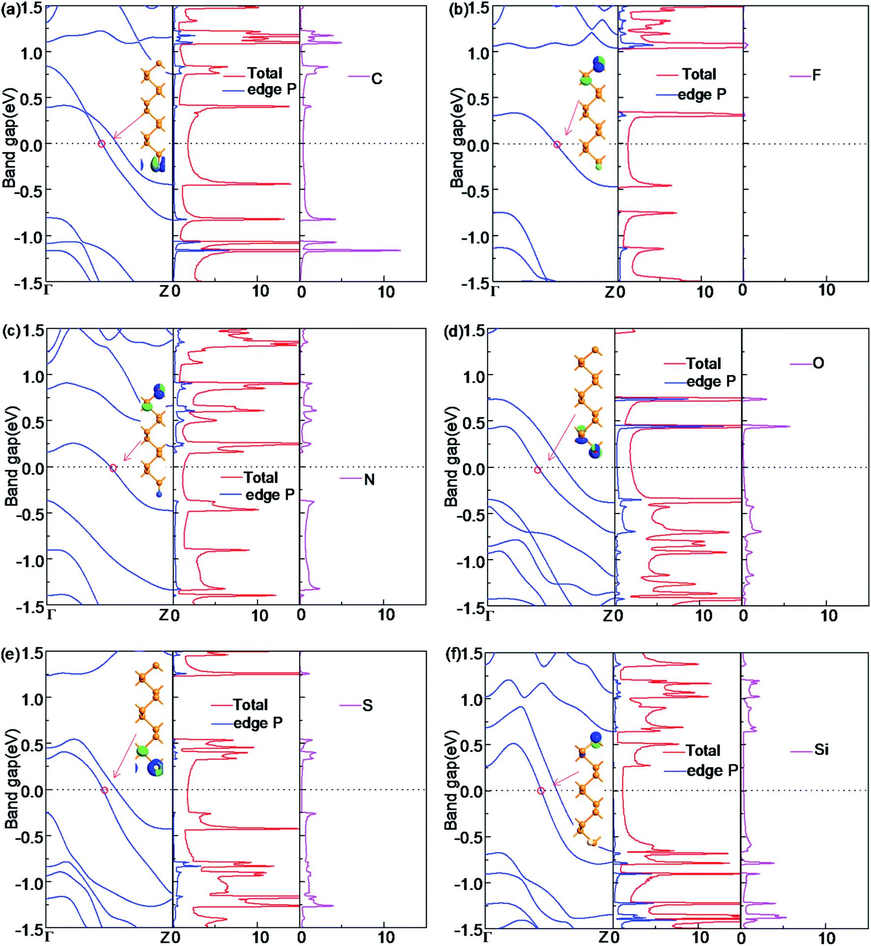 | ||
| Fig. 4 The band structure (BS), the total density of states (DOS) and atom-projected density of states (PDOS), and the Bloch state of X-ZPNR for (a) C-ZPNR, (b) F-ZPNR, (c) N-ZPNR, (d) O-ZPNR, (e) S-ZPNR, and (f) Si-ZPNR. | ||
3.4 The effect of in-plane transverse electric field
For the field-effect-transistor application, a large on/off ratio is required. This requires that the electronic structure should be sensitive to the gate voltage or external electric field as large as possible. To this end, we investigate the band modulation of PNRs by an external electric field which have been confirmed early to be an effective route to tuning electronic properties of nanostructures.1 When an in-plane transverse external electric field is applied along the transverse direction perpendicular to the ribbon direction, significant changes in band structures are induced in ZPNRs. Here, we take F-ZPNR-F, H-ZPNR-H and N-ZPNR-N as examples. As shown in Fig. 5(a), with the increasing transverse electric field, the band gaps of the ZPNRs decrease but with different rates. The bandgap reduction with the increasing electric field can be understood from the Stark effect.29 For the F-ZPNR-F and H-ZPNR-H, without the transverse electric field, the band gap is 1.49 eV and 1.71 eV respectively, but reduces to 0.81 eV and 1.15 eV with 0.5 V Å−1 transverse electric field. The stronger the transverse electric field, the bigger the band gap drops. The change in the N-ZPNR-N ribbon is more apparent: without the transverse electric field, the band gap is 0.66 eV but reduces to 0 eV with 0.3 V Å−1 transverse electric field. The bandgap decreases monotonically with the increasing filed strength. A semiconductor-to-metal transition occurs when the electric field reaches 0.3 V Å−1, which is highly consistent with the previous work. | ||
| Fig. 5 (a) Computed band gaps versus the in-plane transverse electric field for the ZPNR. (b) The band structure versus the electric field for N-ZPNR-N. | ||
Fig. 5(b) displays the evolution of the band structure with an electric field ranging from 0.0 to 0.5 V Å−1 for N-ZPNR-N. It can be seen that with the increasing transverse electric field, the conduction band goes down and valence band moves up gradually. Compared to the band structure without electric field (0 V Å−1), the energy bands of the degenerate edge states above the CBM and below the VBM under the electric field show a certain degree of splitting and localization, which pushes the CBM and VBM closer to the Fermi level, leading to the band gap narrowing. These features are very desirable for nano-electronic devices based on ZPNRs where the easy modulation of the electronic structure by transverse electric field is a basic requirement.
3.5 The electronic transport properties of NM-terminated ZPNRs
Finally, we calculate the electronic transport properties of NM terminated ZPNRs. As stated above, the fully bare-edge ZPNR and X-ZPNR-X (X = C, O, S and Si) all show a distinct metallic nature. Here, we select the O-ZPNR-O and S-ZPNR-S as examples to compute their current–voltage characteristics and also compare them with the fully bare-edge ZPNR. Fig. 6 shows the device models constructed from X-ZPNR-X (X = O and S). The device is divided into three regions. The left is an electrode (LE), the right electrode (RE), and the scattering region (SR). Each electrode is represented by a supercell consisting of three repeated X-ZPNR-X unit cells along the transport direction and the scattering region is represented by a supercell with nine repeated X-ZPNR-X unit cells along the transport direction. The fully bare-edge ZPNR device is constructed by the same method. To obtain a stable structure, calculations are performed after the geometry is optimized until all residual forces on each atom are smaller than 0.01 eV Å−1. The transport properties are calculated by using the first-principles software package Atomistix ToolKit (ATK), which is based on density-functional theory (DFT) in combination with the non-equilibrium Green's function (NEGF) method. The related parameters are set to be the same as those stated in Section 2. Once the convergence in the self-consistency calculations is achieved, the current through a device is computed by the Landauer-like formula,30 where T(E,Vb) is the bias dependent transmission coefficient, fL(E,Vb) and fR(E,Vb) the Fermi–Dirac distribution function of the left (L) and right (R) electrode.
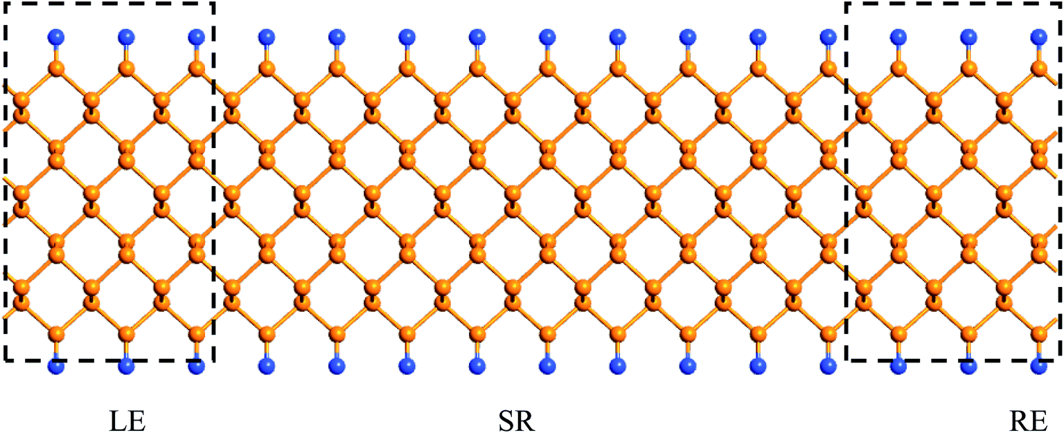 | ||
| Fig. 6 The device models of the ZPNRs with symmetrical edge terminations. The fully bare-edge ZPNRs device is constructed by the same method. | ||
The self-consistently calculated current–voltage (I–V) characteristics are shown in Fig. 7(a). As can be seen, they display significantly different features to one another. We can see that for O-ZPNR-O and S-ZPNR-S devices, the current increases with the bias linearly, especially obvious for the S-ZPNR-S device which demonstrate an Ohmic characteristic with their metallic nature. But for the fully bare-edge ZPNR device, the I–V curve is nonlinear. To identify these results, the transmission spectra for three devices are shown in Fig. 7(b)–(d), respectively. They are the most intuitive representations of electronic structures and transport behaviors of a device. As can be seen, for O-ZPNR-O and S-ZPNR-S devices, the shape of the transmission spectrum curve changes very little with the increasing bias, especially in the bias window. According to Landauer-like formula, the current is the integration of the transmission spectrum in the bias window. As a result, such an integration area increases monotonically with the bias. This is the reason why the I–V curves for O-ZPNR-O and S-ZPNR-S devices are linear versus bias. While for the fully bare-edge ZPNR device, the situation is quite different. The transmission coefficients within the bias windows undergo a prominent decrease with the increasing bias. This obvious bias effect might be caused by the dangling-bond edge states of P atoms being very sensitive to the bias, as the nanoribbon is polarized by the electric field effect. When the expanding rate of the bias window region cannot compensates the decreasing speed of transmission coefficients, the current drops with the bias. In short, our calculations show that the introduction of NM atoms as terminations can effectively enhance the transport properties of ZPNRs.
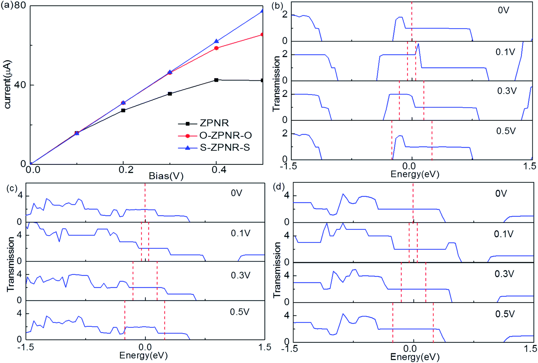 | ||
| Fig. 7 (a) The I–V characteristics for bare-edge ZPNR, O-ZPNR-O and S-ZPNR-S respectively. The transmission spectra of these three models under several typical biases, (b) for the fully bare-edge ZPNR, (c) for O-ZPNR-O, and (d) for S-ZPNR-S. | ||
4. Conclusion
The electronic properties of zigzag phosphorene nanoribbons (ZPNRs) terminated with nonmetallic (NM) atoms H, F, C, N, O, S and Si are studied systematically using the first-principles method based on the density-functional theory and nonequilibrium Green's function. Several possible cases are considered, ZPNRs with the symmetrical edge terminations of NM atoms, asymmetrical edge terminations of H passivating one edge and NM atoms terminating another edge, and the half-bare edge case where only one edge is terminated with NM atoms while the other edge remains bare. The results show that the fully bare-edge ZPNR is a metal; and the ZPNRs terminated with C, O, S and Si are always a metal regardless of the termination cases because the edge states of the termination atoms are located at the Fermi level. For the ZPNRs terminated with F and N at both sides or with F and N at one edge while H at the other edge, the electronic structures are found to be semiconducting because the edge states of the termination atoms are located at the position far from the Fermi level. In the case of the half-bare edges, the electronic structures of the ribbons are metallic. The ribbons with edge modification of C, F, N, O, S and Si atoms are more stable than the H-terminated ZPNR. For the F-ZPNR-F, H-ZPNR-H and N-ZPNR-N, with the increasing transverse electric field, the band gaps of the ZPNRs decrease but with different rates and a semiconductor-to-metal transition occurs for the N-ZPNR-N.In addition, we also constructed some nanodevices consisting of ZPNRs terminated respectively by O and S at both edges and being fully bare-edge. It is found that O and S terminated ZPNRs device have a good linear response to the bias, and the current is significantly larger than that in the bare edge ZPNRs device. These results indicate that the introduction of NM atoms at edge(s) can effectively modulate the electronic and the transport properties of ZPNRs.
Conflicts of interest
There are no conflicts to declare.Acknowledgements
M. L. would like to thank the National Thousand Talents Award from China. This work was supported by the National Natural Science Foundation of China (Grant No. 51771123, 61371065), the Hunan Provincial Natural Science Foundation of China (Grant No. 2015JJ3002), the Scientific Research Fund of Hunan Provincial Education Department (Grant No. 17C0030), the Open Research Fund of the Hunan Province Higher Education Key Laboratory of Modeling and Monitoring on the Near-Earth Electromagnetic Environments (No. 20160106), Changsha University of Science & Technology.References
- Q. Wu, L. Shen, M. Yang, Y. Q. Cai, Z. G. Huang and Y. P. Feng, Electronic and transport properties of phosphorene nanoribbons, Phys. Rev. B: Condens. Matter Mater. Phys., 2015, 92, 035436 CrossRef.
- Y. Cai, Q. Ke, G. Zhang, B. I. Yakobson and Y.-W. Zhang, Highly Itinerant Atomic Vacancies in Phosphorene, J. Am. Chem. Soc., 2016, 138, 10199–10206 CrossRef CAS PubMed.
- X. Zhang, Q. Li, Bo Xu, Bo Wan, Y. Jiang and X. G. Wan, Tuning carrier mobility of phosphorene nanoribbons by edge passivation and strain, Phys. Lett. A, 2016, 380, 614–620 CrossRef CAS.
- N. Suvansinpan, F. Hussain, G. Zhang, H. C. Cheng, Y. Cai and Y.-W. Zhang, Substitutionally doped phosphorene: electronic properties and gas sensing, Nanotechnology, 2016, 27, 065708 CrossRef PubMed.
- R. Fei, V. Tran and L. Yang, Topologically protected Dirac cones in compressed bulk black phosphorus, Phys. Rev. B: Condens. Matter Mater. Phys., 2015, 91, 195319 CrossRef.
- V. Wang, Y. Kawazoe and W. T. Geng, Native point defects in few-layer phosphorene, Phys. Rev. B: Condens. Matter Mater. Phys., 2015, 91, 045433 CrossRef.
- Y. Cai, Q. Ke, G. Zhang, Y. P. Feng, V. B. Shenoy and Y.-W. Zhang, Giant Phononic Anisotropy and Unusual Anharmonicity of Phosphorene: Interlayer Coupling and Strain Engineering, Adv. Funct. Mater., 2015, 25, 2230 CrossRef CAS.
- Z. Zhu, J. Guan and D. Tománek, Strain-induced metal-semiconductor transition in monolayers and bilayers of gray arsenic: a computational study, Phys. Rev. B: Condens. Matter Mater. Phys., 2015, 91, 161404 CrossRef.
- Carvalho, M. Wang, Xi Zhu, A. S. Rodin, H. Su and A. H. Castro Neto, Phosphorene: from theory to applications, Nat. Rev. Mater., 2016, 1, 16061 CrossRef CAS.
- Batmunkh, M. Bat-Erdene and J. G. Shapter, Phosphorene and Phosphorene-Based Materials – Prospects for Future Applications, Adv. Mater., 2016, 28, 8586–8617 CrossRef CAS PubMed.
- Pang, A. Bachmatiuk, Y. Yin, B. Trzebicka, L. Zhao, L. Fu, R. G. Mendes, T. Gemming, Z. Liu and M. H. Rummeli, Applications of Phosphorene and Black Phosphorus in Energy Conversion and Storage Devices, Adv. Energy Mater., 2018, 8, 1702093 CrossRef.
- Dhanabalan, J. S. Ponraj, Z. Guo, S. Li, Q. Bao and H. Zhang, Emerging Trends in Phosphorene Fabrication towards Next Generation Devices, Adv. Sci., 2017, 4, 1600305 CrossRef PubMed.
- T. Takahashi, H. Tokailin, S. Suzuki, T. Sagawa and I. Shirotani, Electronic Band structure of black phosphorus studied by angle-resolved ultraviolet photoelectron spectroscopy, J. Phys. C: Solid State Phys., 1985, 18(4), 825–836 CrossRef CAS.
- Han, M. Y. Yao, X. X. Bai, L. Miao, F. Zhu, D. D. Guan, S. Wang, C. L. Gao, C. Liu, D. Qian, Y. Liu and J.-f. Jia, Electronic structure of black phosphorus studied by angle-resolved photoemission spectroscopy, Phys. Rev. B: Condens. Matter Mater. Phys., 2014, 90(8), 085101 CrossRef.
- V. Tran, R. Soklaski, Y. Liang and L. Yang, Layer-controlled band gap and anisotropic excitons in few-layer black phosphorus, Phys. Rev. B: Condens. Matter Mater. Phys., 2014, 89(23), 235319 CrossRef.
- N. Rudenko and M. I. Katsnelson, Quasiparticle band structure and tight binding model for single- and bilayer black phosphorus, Phys. Rev. B: Condens. Matter Mater. Phys., 2014, 89(20), 201408 CrossRef.
- A. Hashmi and J. Hong, Transition Metal Doped Phosphorene: First-Principles Study, J. Phys. Chem. C, 2015, 119(17), 9198–9204 CrossRef CAS.
- T. Hu and J. Hong, First-Principles Study of Metal Adatom Adsorption on Black Phosphorene, J. Phys. Chem. C, 2015, 119(15), 8199–8207 CrossRef CAS.
- H. Guo, N. Lu, J. Dai, X. Wu and X. C. Zeng, Phosphorene nanoribbons, nanotubes and van der Waals multilayers, J. Phys. Chem. C, 2014, 118, 14051–14059 CrossRef CAS.
- V. Tran and L. Yang, Scaling Laws of the Band Gap and Optical Response of Phosphorene Nanoribbons, Phys. Rev. B: Condens. Matter Mater. Phys., 2014, 89, 245407 CrossRef.
- X. Peng and Q. Wei, Edge effects on the electronic properties of phosphorene nanoribbons, J. Appl. Phys., 2014, 116, 144301 CrossRef.
- W. Li, G. Zhang and Y.-W. Zhang, Electronic Properties of Edge-Hydrogenated Phosphorene Nanoribbons: A First-Principles Study, J. Phys. Chem. C, 2014, 118(38), 22368–22372 CrossRef CAS.
- J. Taylor, H. Guo and J. wang, Ab initio modeling of quantum transport properties of molecular electronic devices, Phys. Rev. B: Condens. Matter Mater. Phys., 2001, 63, 245407 CrossRef.
- M. Brandbyge, J. L. Mozos, P. Ordejon, J. Taylor and K. Stokbro, Density-functional method for nonequilibrium electron transport, Phys. Rev. B: Condens. Matter Mater. Phys., 2002, 65, 165401 CrossRef.
- J. He, K. Q. Chen, Z. Q. Fan, L. M. Tang and W. P. Hu, Transition from insulator to metal induced by hybridized connection of graphene and boron nitride nanoribbons, Appl. Phys. Lett., 2010, 97, 193305 CrossRef.
- J. Zeng, K. Q. Chen and C. Q. Sun, Electronic structures and transport properties of fluorinated boron nitride nanoribbons, Phys. Chem. Chem. Phys., 2012, 14, 8032 RSC.
- W. Oswald and Z. Wu, Energy gaps in graphene nanomeshes, Phys. Rev. B: Condens. Matter Mater. Phys., 2012, 85, 115431 CrossRef.
- A. Brown and S. Rundqvist, Refinement of the crystal structure of black phosphorus, Acta Crystallogr., 1965, 19, 684 CrossRef CAS.
- J. Kang, F. Wu and J. Li, Modulating the Bandgaps of Graphdiyne Nanoribbons by Transverse Electric Fields, J. Phys.: Condens. Matter, 2012, 24, 165301 CrossRef PubMed.
- R. Landauer, Electrical resistance of disordered one dimensional lattices, Philos. Mag., 1970, 21(172), 863–867 CrossRef CAS.
| This journal is © The Royal Society of Chemistry 2020 |