
 Open Access Article
 This Open Access Article is licensed under a
 Creative Commons Attribution 3.0 Unported Licence
Purity of organic semiconductors as a key factor for the performance of organic electronic devices†
Cigdem
Yumusak
,
Niyazi Serdar
Sariciftci
 and
Mihai
Irimia-Vladu
*
and
Mihai
Irimia-Vladu
*
Linz Institute for Organic Solar Cells (LIOS), Physical Chemistry, Johannes Kepler University Linz, Altenberger Straße 69, 4040 Linz, Austria
First published on 29th October 2020
Abstract
Organic semiconductors offer great promise through their ease of synthesis in a multitude of derivatives, their low temperature processability and their amenability for fabrication of flexible, stretchable and conformable, even imperceptible devices. Nevertheless, the low charge mobility of organic semiconductors remains one of the limiting factors in delivering high performance for organic electronic devices comparable to their inorganic counterparts. In this study, the effects of purification of eight different organic semiconductors (i.e. n-type, p-type, and ambipolar) were determined by means of analyzing their performance improvement in organic field effect transistors. For this purpose, three purity grades of each organic semiconductor were investigated, and devices were fabricated in an identical fashion. It was found that temperature gradient sublimation improves considerably the quality of the organic semiconductors. The results presented here indicate that the purity of the organic semiconductor is a key parameter to be considered in order to achieve high performance for the field of organic field effect transistors.
1. Introduction
In the last two decades, a large effort has been directed towards integration of consumer electronics into emergent “embedded” electronics such as wearable/implantable electronics and internet of things, in other words industry 4.0. The most recent developments include on-tissue sensors, implantable and ingestible medical devices, environmental monitoring, and disposable plastic electronics such as smart food packaging, RFID tags, plastic cards, e-tickets, etc.1–15 All these devices require abundant and inexpensive materials and fabrication technologies supporting their sustainable development. Organic semiconductors are interesting through their synthetic versatility in high throughput at low cost of production. For achieving the coveted goal of “green” and sustainable electronics development, one can tailor and make these materials biocompatible and biodegradable.1,2 The large-scale electronic waste produced in the world is creating trouble in the supply chain of rare earth materials as well as plastic waste contamination in oceans, due to packaging materials in general. Both these unfortunate events can be faced successfully if we introduce biodegradable organic semiconductors, substrates and plastics. However, these materials have to be competitive to the performance requirements. Even though there are large areas of applications which do not need high frequency, high speed transistors and circuits, the mobility of organic semiconductor materials is still lower than their inorganic counterparts. Ultimately, the performance of the selected materials in the functional device will always be a competitive selection parameter parallel to their bio- and eco-friendliness.3The design of new materials with required functional properties has always been a topical issue in Materials science.4–15 It includes both development of useful design rules and reproducible fabrication of new materials, which is particularly important for organic semiconductors to allow for a comprehensive understanding of their structure–property relationships. While studies have shown the great potential of organic materials in attaining excellent performance in optoelectronic devices, combining several functional properties in a single material able to match inorganic counterparts remains challenging.16–20 The organic field effect transistor (OFET) design is remaining still an active research area in organic electronics.19,21–26 In OFETs, every component layer, i.e. the substrate, dielectric, organic semiconductor, contact electrodes, and encapsulation layers, the choice of their materials as well as their geometries, is significant to the ultimate performance of the device.
Back in 2011 there were already crystalline OFETs with the mobility values exceeding those of amorphous silicon27–29 which was the main competitor in the past.21 Nevertheless, reaching values of field effect mobility in excess of 10 cm2 V−1 s−1 remains a tremendous challenge for the design and synthesis of novel organic semiconductors with increased functionalities,20,30 whereas attaining operation frequencies in advanced circuits design in the range of GHz seems possible, but rather difficult to materialize at the same time.31 We argue that all the benefits of inorganic semiconductors can be attributed to three major features of these materials: (i) their extremely high purity, (ii) their long-range order and (iii) their superior coupling through very strong (covalent) bonds. As a matter of fact, all the above beneficial characteristics that represent the cutting edge and the success of inorganic electronics are missing for the classic, i.e. weakly van der Waals bonded, organic semiconductors, where levels of purity of 99% or even lower are tacitly considered as acceptable for the fabrication of organic electronic devices. It is rather surprising that there is to the best of our knowledge no systematic study towards the elucidation of the role of purity of the organic semiconductors for the recorded performance of the fabricated thin film electronic devices. More often than not, organic electronic devices are fabricated with the “as received” materials carrying the declared purity by the chemical supplier,32 this event being obvious from the mere omission of the purification step of the organic semiconductor in the Experimental section of nearly all publications in the field.33–36 Nevertheless, when the effort of purification was invested, then the results improved impressively, with the recorded mobility of the organic semiconductor reaching record values in excess of 5 cm2 V−1 s−1 for single crystal based OFETs with rubrene.37 Importantly also, time of flight measurements at low temperature of ultra-pure oligomeric systems of organic semiconductors showed that mobilities of 10 cm2 V−1 s−1 at room temperature and of several hundred cm2 V−1 s−1 at low temperature are possible to achieve.38
In this work, we tackle the issue of the materials’ purity and its influence on organic electronic devices systematically. We compared here the effect of different materials as well as different purification degrees respectively, on the performance of fabricated devices, to demonstrate systematically the influence of this purification versus performance relationship. We fabricated organic field effect transistors as a tool of evaluation of various purity grades of selected organic semiconductors. For this study a large pool of organic semiconductor materials, with n-, p-, and ambipolar-type charge transport were investigated. The selected semiconductors for this study were: fullerene (C60), pentacene, copper phthalocyanine, indigo (vat blue 1), Tyrian purple, epindolidione, quinacridone and indanthrene blue RS (vat blue 4), the latter 5 molecules belonging to the group of hydrogen bonded (bio)-organic semiconductors.46 We used for the experimental, three grades of purity for each organic semiconductor and fabricated OFETs with the respective materials under identical thin film deposition conditions. The method of purification of the organic semiconductors investigated in this study was the train sublimation method, described previously in detail in other studies.37,39–44 Although the benefit of purification of organic materials for the improvement of their performance was addressed elsewhere,37,39–44 the quantitative results of various purification grades of organic semiconductors of this study clearly and systematically demonstrate that the mobility of charge carriers can be increased orders of magnitude alongside improving other device parameters.
2. Experimental
A photograph of one of the several vacuum sublimation ovens available in our laboratory is presented in Fig. 1. In the particular case displayed in Fig. 1, the sublimed material was quinacridone. The photograph shows by arrows the three important zones of the differential heating oven used for sublimation of the organic semiconductor. Several purification steps are necessary for obtaining a high-quality material, as will be demonstrated throughout this work.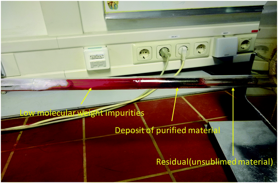 | ||
| Fig. 1 Photograph of the train sublimation oven showing the sublimed material in the vacuum tube. | ||
For the scope of this study, each semiconductor material was analyzed in three purity grades: an unpurified grade (i.e. as-received grade, denoted here as 0×), a one-time purified grade (denoted as 1× in this study) and a three-times purified grade (denoted as 3×). The only exception was Tyrian purple which was synthesized in-house through a previously reported method.45 In this particular case, the entire extracted material was purified scrupulously via column chromatography extraction, and this starting material for our study is designated here as 1×. The successively purified grades employed in this study were 2× and 3× for Tyrian purple.
Sublimation purification of all the semiconductor materials used throughout this study was carried out using a quartz vacuum tube at a pressure below 1 × 10⁻⁶ mbar. A series of borosilicate glass tubes were inserted into the quartz tube and served both to confine the source material and to serve as a vehicle of retrieving the sublimed material. Each material sublimed in a 24 h period at an individual temperature ranging from 250 °C to 400 °C and has been purified by up to three such successive temperature gradient sublimations. Each “as-received” semiconductor was subjected to three successive train sublimation steps in a horizontal vacuum oven, and the purest material was collected after each purification step. The materials collected after the one time and three times sublimation were the ones used in this study, alongside the “as-received” grade. Fullerene (C60) was purchased from Aldrich, product number MKBR 8207 V, having a labeled purity of 99.9%. Pentacene, was purchased from Aldrich, product number P-1802. Copper phthalocyanine was purchased from Sigma, product number 252980. Quinacridone was purchased from TCI Europe, product number Q0057. Epindolidione was purchased from 1-Materials, product number HW1020P1. Indanthrene Blue RS was purchased from TCI Europe, product number I0429. Indigo was purchased from Aldrich, product number 229296, having a labeled purity of 95%. Tyrian purple was synthesized “in-house” following the published synthetic routes.45
When fabricating the devices with each particular grade of purity, we obsessively obeyed all the 9 prerequisites of the reproducibility of results detailed in ref. 46. In short, all devices in this work were fabricated in the same Physical Vapor Deposition (PVD) System, using identical recipes of deposition (vacuum level, temperature ramp, deposition rate, etc.), and in an identical transistor geometry by employing the same shadow masks for the semiconductor structuring, as well as for the gate, source and drain electrode depositions, respectively. Importantly also, there was in this study no attempt made to optimize the results in the sense of adapting the rate of semiconductor deposition (either lower or faster), or play with the substrate heating in order to improve the performance; we used a standard recipe for all eight materials, and fabricated one batch only of 24 transistors for each purity grade of each material in the study. Importantly also, we used an identical dielectric for all materials in this study, namely a bi-layer of inorganic–organic dielectric consisting of electrochemically grown aluminum oxide (AlOx) of 34 nm thickness and a capping layer of tetratetracontane (C44H90 or TTC as acronym) of 20 nm thickness. The anodization method is a standard method employed in our laboratories and was previously described elsewhere.47,48 The thickness of the aluminum gate electrodes that were subjected to anodization was 100 nm for all the devices employed in this study. The respective layer of aluminum was evaporated at a very fast rate of 3–5 nm s−1, which proved beneficial for generating a very smooth layer.49 We used for anodization in this work a recipe that employed passing to the sample to be anodized a step voltage up to a maximum of 20 V, while maintaining in this process a steady current of 15 mA. After reaching the 20 V compliance, the sample was allowed to slowly continue the anodization until the final current read 4.5 μA, which translated to a typical waiting time of about 6–7 min per sample, in our gate geometry. Using this method, as a rule of thumb, one obtains a typical thickness of the anodized layer as
| d = a(V − Vox), |
3. Results
3.1 Organic field effect transistors
The typical device structure utilized in our laboratory employs a staggered bottom gate top contact structure, like the one presented in Fig. 2, with the component layers marked on the figure.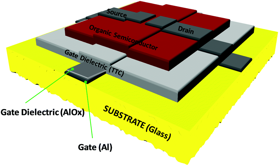 | ||
| Fig. 2 OFET device architecture in the bottom gate-top contact configuration. | ||
The investigated key parameters of organic field-effect transistors are: the operating voltage, the semiconductor charge carrier mobility, the on/off current ratio, the subthreshold swing and finally the threshold voltage and its stability during operation.59Fig. 3 presents an example of a field effect transistor of high mobility fabricated previously in our laboratories.60 It is a device fabricated in a bottom gate-top contact geometry like the one schematically presented in Fig. 2, with adenine capped aluminum oxide as the dielectric layer and fullerene C60 as the organic semiconductor. The graph in Fig. 3(a) shows the recorded transfer characteristics of the OFET, i.e. the measured Idsvs. Vgs at constant Vds voltage, while the one in Fig. 3(b) shows the corresponding output characteristics of the OFET, i.e. the curves measured as Idsvs. Vds at constant Vgs voltages. The important parameters of the device, the ON/OFF ratio and the threshold voltage (Vth) are displayed in the transfer characteristics graph. The average charge mobility of the organic semiconductor in the fabricated batch of which the OFET displayed in Fig. 3 belongs was 3.2 cm2 V−1 s−1.
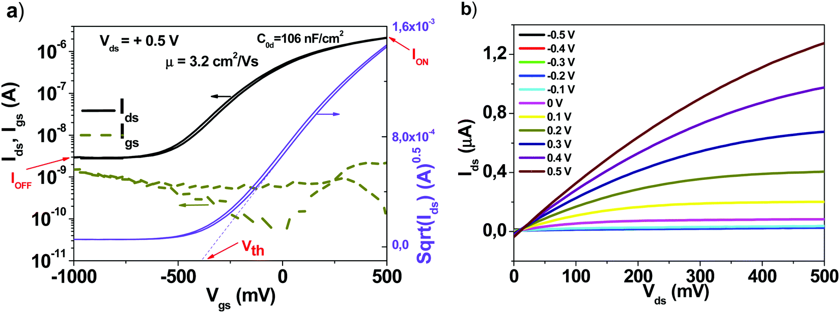 | ||
| Fig. 3 (a) Transfer and (b) output characteristics of an organic field effect transistor which was part of the same batch as the one presented in ref. 60, as Fig. 4(c and d). Adapted with permission from ref. 60, G. Schwabegger, et al., High Mobility, Low Voltage Operating C60 based n-type Organic Field Effect Transistors, Synth. Met., 2011, 161, 2058–2062. | ||
The ON/OFF ratio is the ratio between the current in no conduction mode (marked as IOFF on the graph) and the maximum current attained in the operation (conduction mode, marked as ION on the graph). In the particular example of the device presented in Fig. 3, this ratio is coming close to 1000, or 103. The threshold voltage is determined as the intercept on the horizontal axis of the tangent drawn to the linear part of the square root of the Idsvs. Vgs line in the saturation regime of the transistor (marked as Vth on the graph). For mobility calculations when a straight line is not an accurate fit to the sqrt(Ids) we fitted the line at higher gate voltages. We determined the start and end points of the subthreshold swing from the best straight line fit to a gate voltage interval on the log(Ids) vs. Vgs plot for lower gate voltages than the threshold voltage as discussed in the review paper of Newman et al. (ref. 59).
The field effect mobility of the semiconductor in the saturation regime is extracted from the equation:59
| Ids,sat = (W/2L)Codμsat(Vgs − Vth)2, |
Ssw = 1/Ssl = dVgs/d(log![[thin space (1/6-em)]](https://www.rsc.org/images/entities/char_2009.gif) Ids), Ids), |
| Ssn = Ssw × C0d |
In the above equations Ids,sat represents the drain current in the saturation regime, W and L are the geometric factors of the channel (length, L and width, W, respectively), C0d is the specific capacitance of the dielectric, μsat is the field effect mobility of the organic semiconductor in the saturation regime, Vgs and Vth are the applied gate voltage and the threshold voltage, respectively, and Ssw is the subthreshold swing, expressed in volts per decade of current (i.e. V dec−1). The subthreshold swing indicates how fast the OFET device switches form the OFF to the ON state. It is worth mentioning that the normalized subthreshold swing is a more convenient method to compare the performance of organic semiconductors in OFET devices, when deposited on various dielectrics or on dielectrics of different thicknesses.59 A large value of the subthreshold swing indicates a large concentration of shallow traps, i.e. a slow and non-sharp turn-on region. Given the fact that we have in this study the same dielectric but different purity grades of organic semiconductors, the normalized subthreshold swing values are meaningful as a method of comparison of the performance of dielectric–semiconductor interface within the three purity grades of each semiconductor material.
The schematic of the semiconductor molecules employed in this work is presented in Fig. 4.
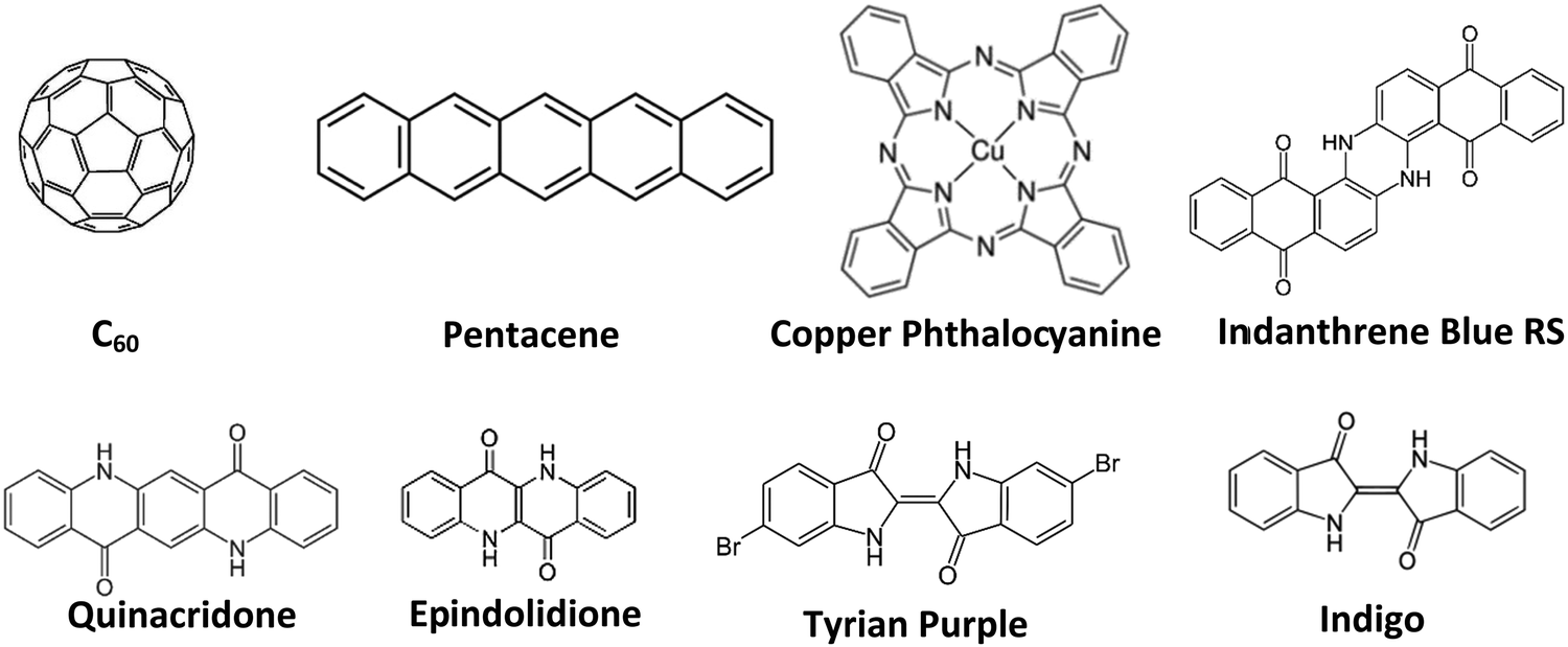 | ||
| Fig. 4 Schematic of the molecules employed in this study. | ||
3.2 Fullerene, C60
The schematic of the C60 molecule is presented in Fig. 4. We fabricated devices with fullerene (C60) and compared the three purity grades mentioned above, i.e. 0×, 1× and 3× in OFET devices. It is interesting to note that although the original (0×) material had a declared purity of 99.9% according to the label on the material package of the chemical supplier (Aldrich), the average mobility obtained for the 24 transistors fabricated was in the range of 5 × 10⁻⁵ cm2 V−1 s−1 (black line in Fig. 5).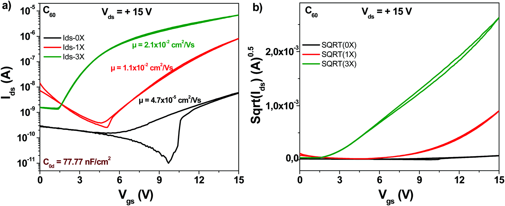 | ||
| Fig. 5 (a) Comparison of OFET devices with three different grades of fullerene (C60) semiconductor purity: unpurified (0× in graph legend), one time purified (1× in graph legend) and three times purified respectively (3× in graph legend); (b) the sqrt(Ids) vs. Vgs of the three purity grades presented in panel (a). | ||
The one-time sublimed material showed a more decent performance, with mobility values already in the range of 1 × 10⁻² cm2 V−1 s−1. One sublimation of fullerene resulted therefore in a 200-fold increase in mobility, while three successive purification steps on the other hand counted for another 4-fold increase in the organic semiconductor mobility compared to the one-time purified grade (in total almost three orders of magnitude compared to the unpurified grade). It is interesting to note also that three steps of material purification decreased the subthreshold swing of the transistor from 4.8 to 1.1 V dec−1. Full details over the transistor's parameters (subthreshold swing, subthreshold slope, ON/OFF ratio and normalized subthreshold swing) are offered in Table 1.
| Semiconductor | Purity grade | Mobility | I on/Ioff | S sw (V dec−1) | S n (VnF cm−2 dec−1) | V th (V) | |
|---|---|---|---|---|---|---|---|
| e− | h+ | Electron (and/or) hole | Electron and/or hole | Electron (and/or) hole | Electron (and/or) hole | ||
| Fullerene (C60) | Unpurified | 4.7 × 10⁻⁵ | — | 18 | 4.9 | 381 | 8.7 |
| Purified* | 1.1 × 10⁻² | — | 1.8 × 10³ | 2.6 | 202.2 | 8.5 | |
| Purified*** | 4.5 × 10⁻² | — | 5 × 10³ | 1.2 | 93.3 | 0.75 | |
| Pentacene | Unpurified | — | 1.9 × 10⁻⁴ | 5.7 × 10² | 2.5 | 194.4 | −4 |
| Purified* | — | 7.5 × 10⁻⁴ | 1.4 × 10³ | 2.3 | 178.9 | −3.5 | |
| Purified*** | — | 2 × 10⁻² | 4.4 × 10² | 1.4 | 109 | −1 | |
| Copper phthalocyanine | Unpurified | — | 2.6 × 10⁻⁵ | 39 | 4.1 | 318.5 | −9.5 |
| Purified* | — | 9.2 × 10⁻⁴ | 1.1 × 10³ | 1.9 | 147.8 | −6.75 | |
| Purified*** | — | 2.1 × 10⁻³ | 3 × 10³ | 1.7 | 132.2 | −5 | |
| Indanthrene blue | Unpurified | 1.5 × 10⁻⁴ | 5.4 × 10⁻⁴ | 79 | 3.7 | 287.7 | −4.5 |
| 37.2 | 2.7 | 210 | −9.5 | ||||
| Purified* | 9.4 × 10⁻⁴ | 5.9 × 10⁻³ | 48 | 2.8 | 217.7 | −4.5 | |
| 38 | 2.9 | 225.5 | −5.5 | ||||
| Purified*** | 2 × 10⁻³ | 1.6 × 10⁻² | 55 | 2.4 | 186.6 | −8.5 | |
| 207 | 1.6 | 124.4 | −9 | ||||
| Quinacridone | Unpurified | — | 4.7 × 10⁻⁵ | 87.2 | 3.3 | 256.6 | −9.5 |
| Purified* | — | 1.3 × 10⁻³ | 6 × 10² | 1.9 | 147.7 | −8.75 | |
| Purified*** | — | 9.8 × 10⁻³ | 2.8 × 10³ | 1.2 | 93.3 | −6 | |
| Epindolidione | Unpurified | — | 4.4 × 10⁻⁶ | 3.5 | 11.3 | 878.8 | −11 |
| Purified* | — | 8.3 × 10⁻³ | 1.3 × 10⁴ | 2.2 | 171 | −7.5 | |
| Purified*** | — | 9.7 × 10⁻² | 3.5 × 10⁴ | 1.9 | 147.8 | −4.9 | |
| Tyrian purple | Purified* | 6.5 × 10⁻⁵ | 9.2 × 10⁻⁴ | 13 | 4.6 | 357.7 | −6 |
| 303 | 2 | 155.5 | −9.75 | ||||
| Purified** | 3.1 × 10⁻⁴ | 2.1 × 10⁻³ | 41 | 3.2 | 248.9 | −7.5 | |
| 1.4 × 10³ | 1.3 | 101.1 | −9 | ||||
| Purified*** | 6.8 × 10⁻⁴ | 3.8 × 10⁻³ | 63 | 2.8 | 217.7 | −3 | |
| 2 × 10³ | 1.1 | 85.5 | −8 | ||||
| Indigo | Unpurified | 2 × 10⁻³ | 7 × 10⁻⁵ | 3 × 10³ | 2.7 | 235 | 8 |
| 287 | 1.9 | 165.3 | −5 | ||||
| Purified* | 3 × 10⁻³ | 9 × 10⁻⁴ | 7.8 × 10³ | 1.7 | 148 | 5 | |
| 3.4 × 10³ | 2.2 | 191.4 | 0.5 | ||||
| Purified*** | 1.5 × 10⁻² | 1.2 × 10⁻² | 1.1 × 10⁴ | 1.2 | 104.4 | 4.5 | |
| 5.9 × 10³ | 1.3 | 113.1 | −2 | ||||
3.3 Pentacene
The schematic of the pentacene molecule is displayed in Fig. 4. The OFET transistor characteristics are presented in Fig. 6. Different than C60 though, the one-time purified grade does not show a major improvement in transistor mobility as compared to the unpurified grade, i.e. only a 4-fold increase, from 1.9 × 10⁻⁴ to 7.5 × 10⁻⁴ cm2 V−1 s−1. Nevertheless, the three times purified grade of pentacene shows a marked increase in mobility that reached 2 × 10⁻² cm2 V−1 s−1 (100-fold compared to the unpurified grade). At the same time, the three times purified material showed a significant decrease of the subthreshold swing compared to the unpurified material, i.e. from 2.5 to 1.4 V dec−1, with full details of the transistor measurements offered in Table 1.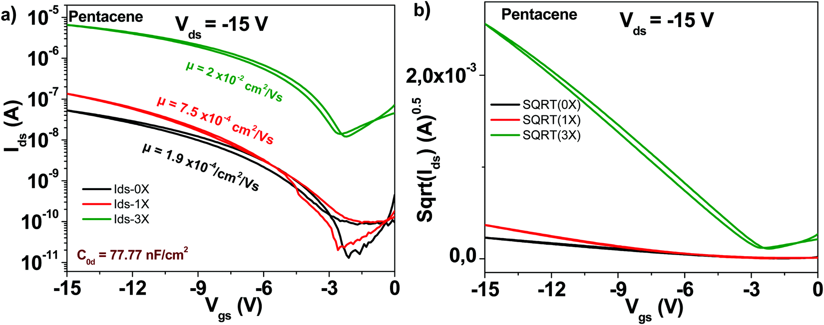 | ||
| Fig. 6 (a) Comparison of OFET devices with three different purity grades of pentacene semiconductor: unpurified (0× in graph legend), one time purified (1× in graph legend) and three times purified respectively (3× in graph legend); (b) the sqrt(Ids) vs. Vgs of the three purity grades presented in panel (a). | ||
3.4 Copper phthalocyanine
The schematic of the copper phthalocyanine molecule is displayed in Fig. 4. OFET devices employing the “as received” grade showed as in the case of fullerene and pentacene a modest mobility value, in the range of 2 × 10⁻⁵ cm2 V−1 s−1 (see Fig. 7). However, one single step of purification resulted in a charge mobility increase of 35-fold, to 9 × 10⁻⁴ cm2 V−1 s−1. Two more purification steps made possible attaining a mobility of 2 × 10⁻³ cm2 V−1 s−1, in other words an 80-fold increase from the original, unpurified material. Notably, the subthreshold swing decreased from 4.1 V dec−1 to 1.6 V dec−1 after three sublimation steps. Full details of the subthreshold parameters as well as the ON/OFF ratios and threshold voltages for the OFETs featuring the three purity grades of copper phthalocyanine OFETs are presented in Table 1.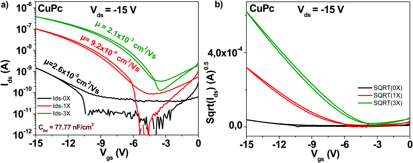 | ||
| Fig. 7 (a) Comparison of OFET devices with three different purity grades of copper phthalocyanine semiconductor: unpurified (0× in graph legend), one time purified (1× in graph legend) and three times purified, respectively (3× in graph legend); (b) the sqrt(Ids) vs. Vgs of the three purity grades presented in panel (a). | ||
3.5 Indanthrene blue RS
Indanthrene blue RS (vat blue 4) employed in this study has the chemical structure presented in Fig. 4. Different from the previously described materials in this study, indanthrene blue RS is an ambipolar semiconductor when it is deposited on top of aliphatic dielectrics (TTC in this study). Transistor characteristic results of OFETs with indanthrene blue RS semiconductor are displayed in Fig. 8. As in the case of other organic semiconductors employed in this study, three steps of sublimation proved beneficial for the generation of superior transistor characteristics. Starting from an unpurified material with electron and hole mobilities in the range of ∼10−4 cm2 V−1 s−1, three purification steps increased the respective values to ∼2 × 10⁻² cm2 V−1 s−1 for the hole channel and 2 × 10⁻³ cm2 V−1 s−1 for the electron channel, respectively. Notably, the subthreshold swing also decreased from 3.6 to 2.4 V dec−1 for the electron channel and from 2.7 to 1.6 V dec−1 for the hole channel, and full details of the indanthrene blue RS based OFET performance are presented in Table 1.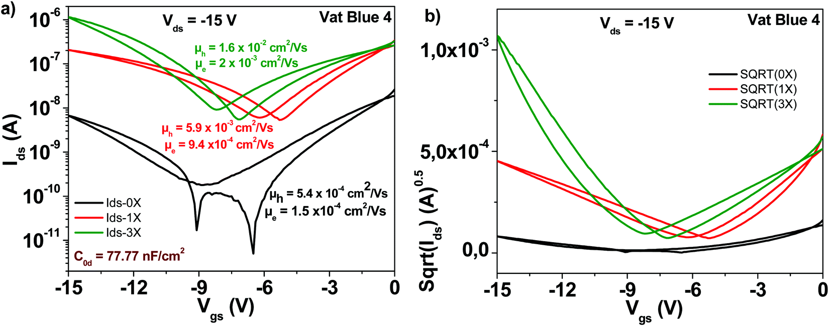 | ||
| Fig. 8 (a) Comparison of OFET devices with three different purity grades of vat blue 4 semiconductor: unpurified (0× in graph legend), one time purified (1× in graph legend) and three times purified, respectively (3× in graph legend); (b) the sqrt(Ids) vs. Vgs of the three purity grades presented in panel (a). | ||
3.6 Quinacridone
The chemical structure of the quinacridone molecule is displayed in Fig. 4. In line with the findings for the previously described semiconductors, also quinacridone displayed a tremendous increase in mobility and decrease of subthreshold swing after three purification steps, see Fig. 9. Starting from a field effect mobility of ∼5 × 10⁻⁵ cm2 V−1 s−1 for an unpurified, “as received” grade, quinacridone's field effect mobility reached ∼1 × 10⁻² cm2 V−1 s−1 for the three times purified grade. At the same time, the subthreshold swing decreased from 3.2 to 1.2 V dec−1 respectively, accompanied by an increase in the ON/OFF ratio from 87 to 2800. Full details of the transistor characteristic parameters are offered in Table 1.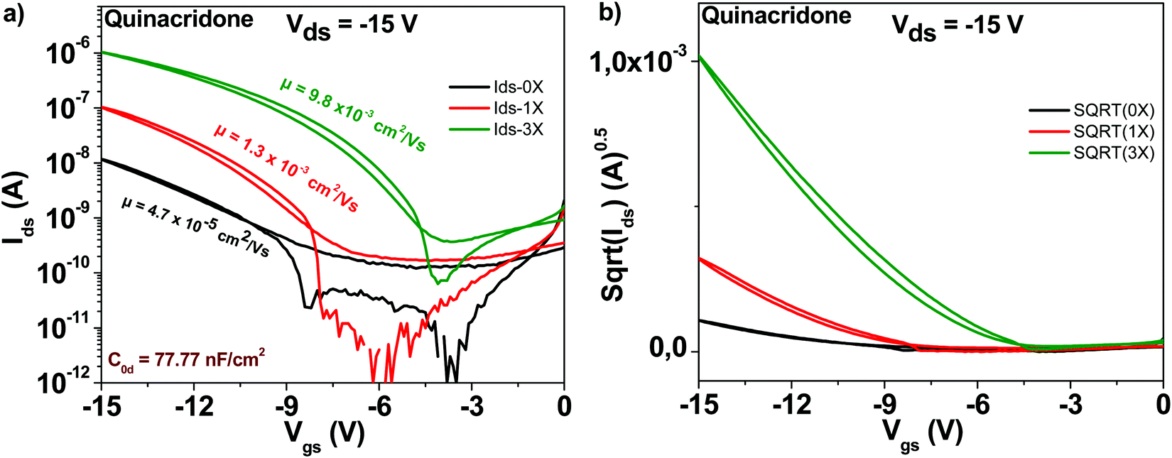 | ||
| Fig. 9 (a) Comparison of OFET devices with three different purity grades of quinacridone semiconductor: unpurified (0× in graph legend), one time purified (1× in graph legend) and three times purified, respectively (3× in graph legend); (b) the sqrt(Ids) vs. Vgs of the three purity grades presented in panel (a). | ||
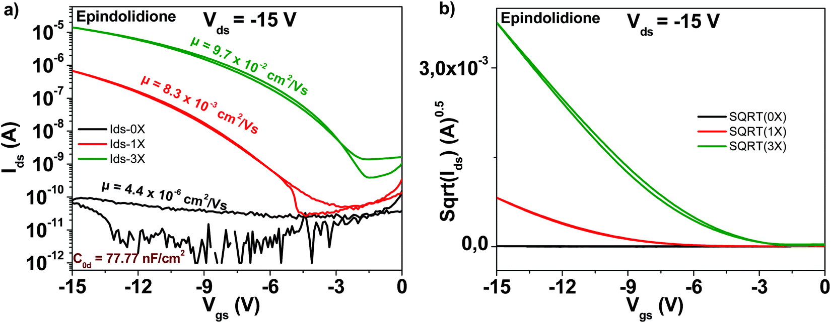
3.7 Epindolidione
The chemical structure of the epindolidione molecule is displayed in Fig. 4. Among the studied materials in this work, epindolidione was the one that produced the most remarkable improvement after being subjected to three steps of purification. Indeed, starting from very low field effect mobility of the “as received” material of 4.4 × 10⁻⁶ cm2 V−1 s−1, epindolidione based OFETs almost reached the mobility of 0.1 cm2 V−1 s−1 after being subjected to three steps of scrupulous purification, or in other words an improvement in excess of 22000. This tremendous mobility improvement was accompanied by a decrease of the subthreshold swing from 11.3 to 1.9 V dec−1 and an increase of the ON/OFF ratio from 3.5 to 3.5 × 10⁴, literally a 10000-fold improvement (Fig. 10). Full details of the transistor characteristics for epindolidione based OFETs with the three grades of analyzed purity are offered in Table 1.
 | ||
| Fig. 10 (a) Comparison of OFET devices with three different purity grades of epindolidione semiconductor: unpurified (0× in graph legend), one time purified (1× in graph legend) and three times purified, respectively (3× in graph legend); (b) the sqrt(Ids) vs. Vgs of the three purity grades presented in panel (a). | ||
3.8 Tyrian purple
A schematic of the Tyrian purple molecule (6,6′-Br-Indigo) is presented in Fig. 4. The results with OFETs carrying the three grades of pure Tyrian purple are displayed in Fig. 11. Given the good purity of Tyrian purple to start with (1×) in this study, it makes full sense that this material displayed the lowest improvement among all the other organic semiconductors analyzed in this study. After three sublimation steps, the electron channel improved by a little bit over one order of magnitude in field effect mobility (i.e. ∼6 × 10⁻⁵ to ∼6 × 10⁻⁴ cm2 V−1 s−1), whereas the hole channel improved by a factor of 4 only (i.e. from ∼9 × 10⁻⁴ to ∼4 × 10⁻³ cm2 V−1 s−1). However, the successive purification steps did indeed improve the material performance, a fact that is obvious in the obtained transistor parameters displayed in Table 1, i.e. the subthreshold swing decreased for the electron channel from 4.6 to 2.8 V dec−1, while for the hole channel from 2 to 1 V dec−1, when comparing the 1× and 3× purity grades.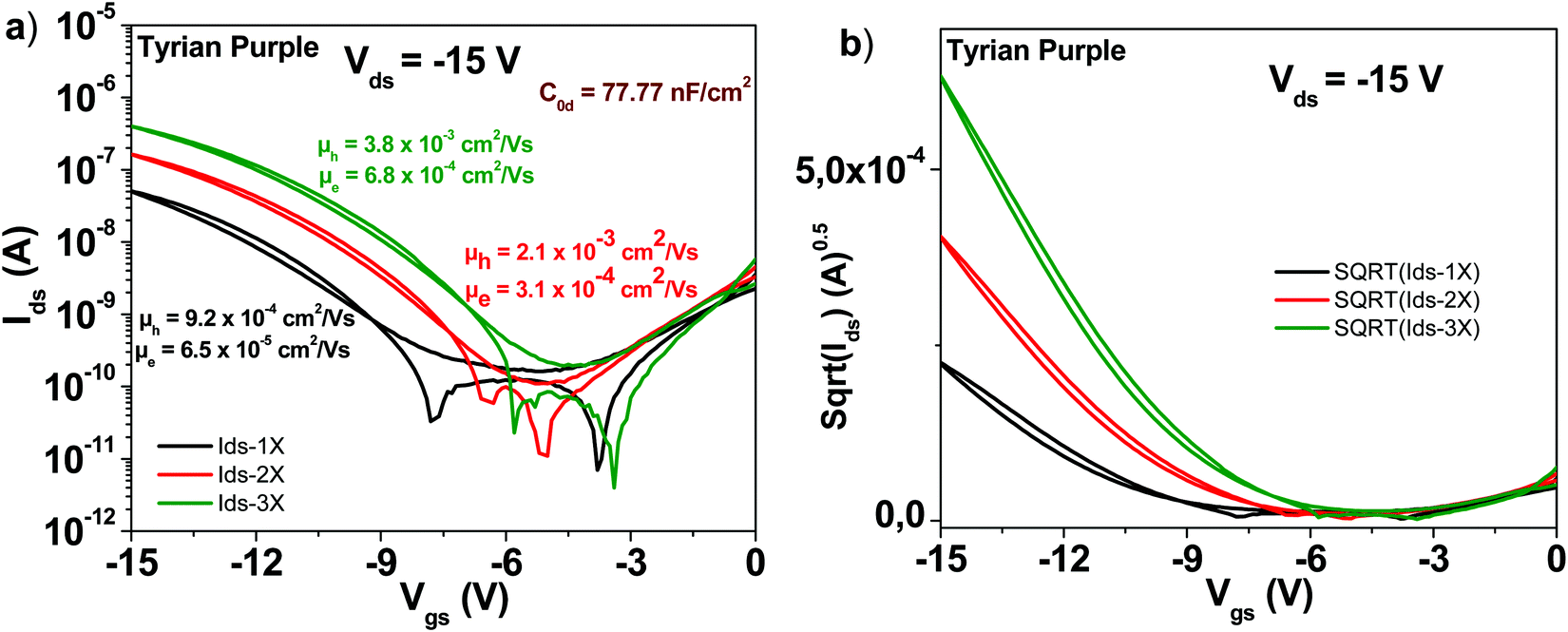 | ||
| Fig. 11 (a) Comparison of OFET devices with three different purity grades of Tyrian purple semiconductor: one-time purified (1× in graph legend), two times purified (2× in graph legend) and three times purified, respectively (3× in graph legend); (b) the sqrt(Ids) vs. Vgs of the three purity grades presented in panel (a). | ||
3.9 Indigo
A schematic of an indigo molecule is presented in Fig. 4. Indigo employed in this study was reported in our previous publication (ref. 46). In this work we present in addition, the tabulated values of the transistor parameters. It is obvious that performing three rounds of purification not only increases the mobility of the semiconductor but also decreases the subthreshold swing from ∼2.7 to 1.2 V dec−1 for the electron channel and from ∼1.9 to 1.3 V dec−1 for the hole channel respectively (see Fig. 12). Full details of the recorded/calculated values of the indigo transistor performance are presented in Table 1.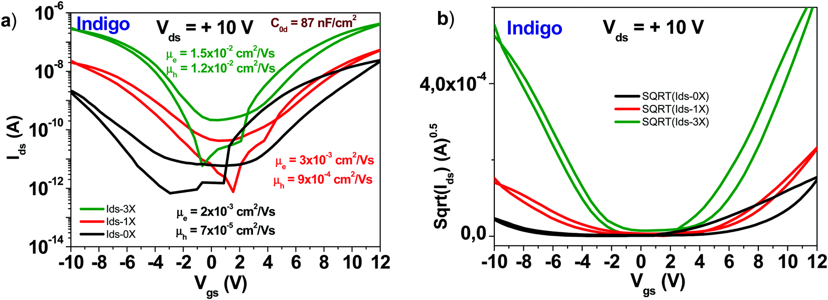 | ||
| Fig. 12 (a) Comparison of OFET devices with three different purity grades of indigo semiconductor: an unpurified grade (0× in graph legend), a one-time purified grade (1× in graph legend) and a three times purified grade, respectively (3× in graph legend). The specific capacitance of Indigo OFETs is 87 nF cm−2; (b) the sqrt(Ids) vs. Vgs of the three purity grades presented in panel (a). Adapted with permission from ref. 46, M. Irimia-Vladu, et al., Chem. Mater., 2019, 31(17), 6315–6346. | ||
4. Discussion and conclusions
We showed here that scrupulous purification of the organic semiconductor is a critical parameter in improving the performance of the organic field effect transistors. We should point out here that each semiconductor material has itself a designated (specific) purification recipe, that differ from one another in the temperature ramping, the differential heating of the vacuum tube, and mostly the flow rate of the carrier gas and its type (Ar, N2, or even no carrier gas, etc.). All these factors are material specific and cannot be generalized. In this work we demonstrated that by pursuing several purification steps starting from the pristine material, all the transistor parameters (apart from for some few exceptions, the threshold voltage, Vth) consistently improved alongside the purity of the organic semiconductors. In several cases (see Table 1) the mobility improvement surpassed three orders of magnitude, whereas the subthreshold swing decreased to values close to 1 V dec−1.Inspecting Fig. 5–12 presenting transistor measurements in this manuscript, as well as Fig. 3 which displayed a high purity C60-based OFET scrupulously optimized for high mobility values, it is interesting to note that for all the analyzed materials, always the highly purified semiconductor grade displays a much higher OFF level on the transfer characteristics as compared to the pristine, non-purified material. This is in a way counterintuitive, since a higher OFF level of the drain current is usually given by impurities (high doping levels). We consider that the change in morphology of the deposited semiconductor has also a significant influence when comparing various purity grades; and also the fact that we measured all the transistors in the accumulation regime (from zero Vgs to negative Vgs values for p-type materials and from zero Vgs to positive Vgs for the n-type semiconductors, C60), a fact of significant influence on the OFF level of the drain current, observed also by Horowitz et al.61 We went on and measured our devices also in the depletion mode, and observed indeed a tendency of Ioff to move towards lower values, as pointed out by Horowitz et al. This trend is shown by all purity grades of each material and by all materials in this study. It seems plausible to assume then that the change of the morphology of the deposited film due to the increased purity level of the evaporated material generates a film of increased bulk conductivity, which more than offsets the decrease of the Ioff level due to the lower impurity content of the film. More studies will be necessary to elucidate this observed event.
Also, it looks obvious that the identical recipe utilized in this work with respect to the semiconductor deposition is not beneficial for all of them in extracting the maximum performance (i.e. charge mobility value or charge mobility balance of the electron and hole channels, as it is the case for Tyrian purple or indanthrene blue RS). For all materials, a specific deposition method has to be implemented for rendering the high performance.52,56,57,60 In this respect, several factors need to be carefully considered and optimized for maximum performance of each material in OFETs, like for example: the deposition rate; the substrate temperature during deposition (ideal for the growth of larger crystals which minimizes the number of grain boundaries and the afferent charge trapping sites); the distance from the crucible to the substrate holder, the semiconductor layer thickness, etc. As it is visible in Fig. 3 of our already published device,60 a thicker layer of C60 (300 nm in the respective case), carried out in a very deep vacuum of ∼10−9 bar, at a very low rate of deposition, significantly below 1 Å s−1 and a constant substrate temperature of 150 °C seems to be an ideal recipe to obtain high semiconductor mobility performance, in spite of the poor transistor geometry of a large channel of 80 μm utilized there. It is important to mention that this study focused on showing the trend of improvement in the OFET performance via increasing level of purity of organic semiconductors, and not to engineer record values of charge mobility. This is valid also in our choice of the organic dielectric capping layer, i.e. the thin TTC deposited on top of the aluminum oxide dielectric, which does not afford a substrate heating in excess of 65 °C, whereas typical values of substrate heating in excess of 100 °C are required for obtaining high mobility semiconductors, as we showed already in one of our previous studies.60 Obviously, particular deposition recipes can be made available for each semiconductor to extract high charge carrier mobility, as we proved earlier in the case of epindolidione,56 quinacridone,56 indigo58 and Tyrian purple.52 Nevertheless, even though all these factors shall be considered, one will always observe that record values are obtained when the level of cross contamination is minimized, i.e. the vacuum deposition instrument is dedicated for a single material only or cleaned rigorously in-between the change of materials and subsequently utilized for a single material for an extended time. This was indeed the case of C60 deposition in our study in ref. 60, where the organic evaporator instrument was dedicated to handling one material only, i.e. C60 for a very long period of time.
In conclusion, we showed through this study that the purification of organic semiconductors is a critical parameter, resulting in fabricated devices of superior performance. Therefore, we propose that setting a “materials’ purity standard” in different labs worldwide will make the results much more reproducible, comparable and competitive. This could bring a leap forward for organic electronics science and technology.
Conflicts of interest
There are no conflicts to declare.Acknowledgements
We gratefully acknowledge the financial support of the Austrian Science Foundation (FWF) within the Wittgenstein Prize for Prof. Sariciftci (Z222-N19).References
- M. Irimia-Vladu, E. D. Glowacki, N. S. Sariciftci and S. Bauer, Green Materials for Electronics, Wiley-VCH, 2018, ISBN: 978-3-527-33865-8 Search PubMed.
- X. Wu, et al., Thermally stable, biocompatible, and flexible organic field-effect transistors and their application in temperature sensing arrays for artificial skin, Adv. Funct. Mater., 2015, 25, 2138–2146 CrossRef CAS.
- B. Stadlober, M. Zirlk and M. Irimia-Vladu, Route towards sustainable smart sensors: ferroelectric polyvinylidene fluoride-based materials and their integration in flexible electronics, Chem. Soc. Rev., 2019, 48(6), 1787–1825 RSC.
- Handbook of Organic Electronics and Photonics, ed. H. S. Nalwa, ASP Publishers, 2008, ISBN: 1-58883-095-0 Search PubMed.
- Organic Eletronics, ed. H. Klauk, Wiley-VCH, 2006, ISBN: 978-3-527-31264-1 Search PubMed.
- Optoelectronics of Molecules and Polymers, ed. A. Moliton, Springer, Berlin, 2006, ISBN: 0-387-23710-0 Search PubMed.
- Introduction to Organic Electronic and Optoelectronic Materials and Devices, ed. S.-S. Sun and L. R. Dalton, Taylor and Francis, 2008, ISBN: 978-0-8493-9284-9 Search PubMed.
- Flexible Electronics, ed. W. S. Wong and A. Salleo, Springer Berlin, 2009, ISBN: 978-0-387-74362-2 Search PubMed.
- Organic Electronics in Sensors and Biotechnology, ed. R. Shinar and J. Shinar, McGraw Hill, 2009, ISBN: 978-0-07-159675-6 Search PubMed.
- Organic Field Effect Transistors, ed. Z. Bao and J. Locklin, Taylor and Francis, 2007, ISBN: 978-0-8493-8080-8 Search PubMed.
- J. C. Martins and L. A. Sousa, Bioelectronic Vision World Scientific, 2009, ISBN: 978-981-279-430-7 Search PubMed.
- Organic Light Emitting Materials and Devices, ed. Z. Li and H. Meng, Taylor and Francis, 2007, ISBN: 978-1-57444-574-9 Search PubMed.
- Organic Photovoltaics, ed. C. Brabec, V. Dyakonov, J. Parisi and N. S. Sariciftci, Springer Verlag, 2003, ISBN: 3-540-00405 Search PubMed.
- Organic Photovoltaics: Mechanisms, Materials and Devices, ed. S.-S. Sun and N. S. Sariciftci, CRC Press (Taylor & Francis Group), 2005, ISBN: 0-8247-5963-X Search PubMed.
- Physics of Organic Semiconductors, ed. W. Brütting, Wiley VCH, 2005, ISBN: 978-3-527-40550-3 Search PubMed.
- L. Sun, Y. A. Diaz-Fernandez, T. A. Gschneidtner, F. Westerlund, S. Lara-Avila and K. Moth-Poulsen, Single-molecule electronics: from chemical design to functional devices, Chem. Soc. Rev., 2014, 43, 7378–7411 RSC.
- A. Facchetti, π-Conjugated polymers for organic electronics and photovoltaic cell applications, Chem. Mater., 2011, 23, 733–758 CrossRef CAS.
- V. R. Feig, H. Tran and Z. Bao, Biodegradable polymeric materials in degradable electronic devices, ACS Cent. Sci., 2018, 4(3), 337–348 CrossRef CAS.
- C. Wang, H. Dong, W. Hu, Y. Liu and D. Zhu, Semiconducting π-conjugated systems in field-effect transistors: a material odyssey of organic electronics, Chem. Rev., 2012, 112, 2208–2267 CrossRef CAS.
- J. Mei, Y. Diao, A. L. Appleton, L. Fang and Z. Bao, Integrated materials design of organic semiconductors for field-effect transistors, J. Am. Chem. Soc., 2013, 135(18), 6724 CrossRef CAS.
- H. Sirringhaus, Organic field-effect transistors: the path beyond amorphous silicon, Adv. Mater., 2014, 26, 1319–1335 CrossRef CAS.
- S. Z. Bisri, C. Piliego, J. Gao and M. A. Loi, Outlook and emerging semiconducting materials for ambipolar transistors, Adv. Mater., 2014, 26, 1176 CrossRef CAS.
- P. Bujak, I. Kulszewicz-Bajer, M. Zagorska, V. Maurel, I. Wielgus and A. Pron, Polymers for electronics and spintronics, Chem. Soc. Rev., 2013, 42, 8895–8999 RSC.
- H. Dong, X. Fu, J. Liu, Z. Wang and W. Hu, Key points for high-mobility organic field-effect transistors, Adv. Mater., 2013, 25, 6158–6183 CrossRef CAS.
- C. Di, F. Zhang and D. Zhu, Multi-functional integration of OFETs: advances and perspectives, Adv. Mater., 2013, 25, 313–330 CrossRef CAS.
- M. Nikolka, I. Nasrallah, B. Rose, M. K. Ravva, K. Broch, A. Sadhanala, D. Harkin, J. Charmet, M. Hurhangee, A. Brown, S. Illig, P. Too, J. Jongman, I. McCulloch, J.-L. Bredas and H. Sirringhaus, High operational and environmental stability of high-mobility conjugated polymer field-effect transistors through the use of molecular additives, Nat. Mater., 2017, 16, 356–362 CrossRef CAS.
- Organic Electronics, ed. G. Meller and T. Grasser, Springer Berlin, 2010 Search PubMed.
- Semiconducting and Conducting Polymers, ed. A. Heeger, N. S. Sariciftci and E. Namdas, Oxford University Press, 2010 Search PubMed.
- F. C. Grozema and L. D. A. Siebbeles, Mechanism of charge transport in self-organizing organic materials, Int. Rev. Phys. Chem., 2008, 27, 87–138 Search PubMed.
- M. E. Gershenson, V. Podzorov and A. F. Morpurgo, Electronic transport in single-crystal organictransistors, Rev. Mod. Phys., 2006, 78, 973–989 CrossRef CAS.
- H. Klauk, Will we see gigahertz organic transistors?, Adv. Electron. Mater., 2018, 4(10), 1700474 CrossRef.
- J. Zaumseil and H. Sirringhaus, Electron and ambipolar transport in organic field-effect transistors, Chem. Rev., 2007, 107, 1296–1323 CrossRef CAS.
- M. Irimia-Vladu and J. W. Fergus, Impedance spectroscopy of thin films of emeraldine base polyaniline and its implications for chemical sensing, Synth. Met., 2006, 156(21–24), 1396–1400 CrossRef CAS.
- E. F. Gomez, V. Venkatraman, J. G. Grote and A. J. Steckl, DNA bases thymine and adenine in bio-organic light emitting diodes, Sci. Rep., 2014, 4, 7105 CrossRef CAS.
- U. Zschieschang, T. Yamamoto, K. Takimiya, H. Kuwabara, M. Ikeda, T. Sekitani, T. Someya and H. Klauk, Organic electronics on banknotes, Adv. Mater., 2011, 23, 654–658 CrossRef CAS.
- T. R. Ray, J. Choi, A. J. Bandodkar, S. Krishnan, P. Gutruf, L. Tian, R. Ghaffari and J. A. Rogers, Bio-integrated wearable systems: a comprehensive review, Chem. Rev., 2019, 119(8), 5461–5533 CrossRef CAS.
- R. W. I. de Boer, M. E. Gershenson, A. F. Morpurgo and V. Podzorov, Organic single-crystal field-effect transistors, Phys. Status Solidi A, 2004, 201(6), 1302–1331 CrossRef CAS.
- N. Karl, K.-H. Kraft, J. Marktanner, M. Münch, F. Schatz, R. Stehle and H.-M. Uhde, Fast electronic transport in organic molecular solids?, J. Vac. Sci. Technol., A, 1999, 17, 2318 CrossRef CAS.
- A. R. McGhie, A. F. Garito and A. J. Heeger, A gradient sublimer for purification and crystal growth of organic donor and acceptor molecules, J. Cryst. Growth, 1974, 22, 295–297 CrossRef CAS.
- H. J. Wagner, R. O. Loutfy and C.-K. Hsiao, Purification and characterization of phthalocyanines, J. Mater. Sci., 1982, 17, 2781–2791 CrossRef CAS.
- C. D. Dimitrakopoulos, A. R. Brown and A. Pomp, Molecular beam deposited thin films of pentacene for organic field effect transistor applications, J. Appl. Phys., 1996, 80, 2501 CrossRef CAS.
- Y.-Y. Lin, D. J. Gundlach, S. F. Nelson and Th. N. Jackson, Pentacene-based organic thin-film transistors, IEEE Trans. Electron Devices, 1997, 44(8), 1325–1331 CrossRef CAS.
- R. A. Laudise, Ch Kloc, P. G. Simpkins and T. Siegrist, Physical vapor growth of organic semiconductors, J. Cryst. Growth, 1998, 187, 449–454 CrossRef CAS.
- J. Mizuguchi, An improved method for purification of copper phthalocyanine, Cryst. Res. Technol., 1981, 16, 695–700 CAS.
- G. Voss and H. Gerlach, Regioselektiver brom/lithium-Austausch bei 2,5-dibrom-1-nitrobenzol. – Eine einfache synthese von 4-Brom-2-nitrobenzaldehyd und 6,6′-Dibromindigo, Chem. Ber., 1989, 122, 1199–1201 CrossRef CAS.
- M. Irimia-Vladu, Y. Kanbur, F. Camaioni, C. Yumusak, A. A. Vlad, C. V. Irimia, A. Operamolla, G. Farinola, G. Romanazzi, G. P. Suranna, N. González, M. C. Molina, L. F. Bautista, H. Langhals, E. D. Glowacki and N. S. Sariciftci, Stability of selected hydrogen-bonded semiconductors in organic electronic devices, Chem. Mater., 2019, 31(17), 6315–6346 CrossRef CAS.
- L. A. Majewski, M. Grell, S. D. Ogier and J. Veres, A novel gate insulator for flexible electronics, Org. Electron., 2003, 4, 27–32 CrossRef CAS.
- M. Irimia-Vladu, P. A. Troshin, M. Reisinger, G. Schwabegger, M. Ullah, R. Schwoediauer, A. Mumyatov, M. Bodea, J. W. Fergus, V. F. Razumov, H. Sitter, S. Bauer and N. S. Sariciftci, Environmentally sustainable organic field effect transistors, Org. Electron., 2010, 11, 1974–1990 CrossRef CAS.
- A. I. Mardare, M. Kaltenbrunner, N. S. Sariciftci, S. Bauer and A. W. Hassel, Ultra-thin anodic alumina capacitor films for plastic electronics, Phys. Status Solidi A, 2012, 209(5), 813–818 CrossRef CAS.
- M. Kaltenbrunner, T. Sekitani, J. Reeder, T. Yokota, K. Kuribara, T. Tokuhara, M. Drack, R. Schwödiauer, I. Graz, S. Bauer-Gogonea, S. Bauer and T. Someya, An ultra-lightweight design for imperceptible plastic electronics, Nature, 2013, 499, 458–463 CrossRef CAS.
- E. D. Glowacki, L. N. Leonat, G. Voss, M. Badea, Z. Bozkurt, M. Irimia-Vladu, S. Bauer and N. S. Sariciftci, Ambipolar organic field effect transistors and inverters with the natural material tyrian purple, AIP Adv., 2011, 1, 042132 CrossRef.
- Y. Kanbur, M. Irimia-Vladu, E. D. Glowacki, M. Baumgartner, G. Schwabegger, L. N. Leonat, M. Ullah, H. Sitter, R. Schwödiauer, Z. Kücükyavuz, S. Bauer and N. S. Sariciftci, Vacuum processed polyethylene as a dielectric for low voltage operating organic field effect transistors, Org. Electron., 2012, 13, 919–924 CrossRef CAS.
- M. Irimia-Vladu, N. Marjanovic, M. Bodea, G. Hernandez-Sosa, A. Montaigne Ramil, R. Schwödiauer, S. Bauer, N. S. Sariciftci and F. Nüesch, Small-molecule vacuum processed melamine-C60, organic field-effect transistors, Org. Electron., 2009, 10(3), 408–415 CrossRef CAS.
- A. Petritz, A. Fian, E. D. Głowacki, N. S. Sariciftci, B. Stadlober and M. Irimia-Vladu, Ambipolar inverters with natural origin organic materials as gate dielectric and semiconducting layer, Phys. Status Solidi RRL, 2015, 9, 358–361 CrossRef CAS.
- Y. Kanbur, H. Coskun, E. D. Głowacki, M. Irimia-Vladu, N. S. Sariciftci and C. Yumusak, High temperature stability of organic thin-film transistors based on quinacridone pigments, Org. Electron., 2019, 66, 53–57 CrossRef CAS.
- E. D. Glowacki, M. Irimia-Vladu, M. Kaltenbrunner, J. Gąsiorowski, M. S. White, G. Romanazzi, G. P. Suranna, P. Mastrorilli, T. Sekitani, S. Bauer, T. Someya, L. Torsi and N. S. Sariciftci, Hydrogen-bonded semiconducting pigments for air-stable field-effect transistors, Adv. Mater., 2013, 25, 1563–1569 CrossRef CAS.
- A. Petritz, A. Wolfberger, A. Fian, T. Griesser, M. Irimia-Vladu and B. Stadlober, Cellulose derivative based gate dielectric for high performance organic complementary inverters, Adv. Mater., 2015, 27, 7645–7656 CrossRef CAS.
- M. Irimia-Vladu, E. D. Glowacki, P. A. Troshin, D. K. Susarova, O. Krystal, G. Schwabegger, M. Ullah, Y. Kanbur, M. A. Bodea, V. F. Razumov, H. Sitter, S. Bauer and N. S. Sariciftci, Indigo-a natural pigment for high performance ambipolar organic field effect transistors and circuits, Adv. Mater., 2012, 24(3), 375–380 CrossRef CAS.
- C. R. Newman, C. D. Frisbie, D. A. da Silva Filho, J. L. Bredas, P. C. Ewbank and K. R. Mann, Introduction to organic thin film transistors and design of n-channel organic semiconductors, Chem. Mater., 2004, 16, 4436–4451 CrossRef CAS.
- G. Schwabegger, M. Ullah, M. Irimia-Vladu, M. Reisinger, Y. Kanbur, R. Ahmed, P. Stadler, S. Bauer, N. S. Sariciftci and H. Sitter, High mobility, low voltage operating C60 based n-type organic field effect transistors, Synth. Met., 2011, 161, 2058–2062 CrossRef CAS.
- G. Horowitz, R. Hajlaoui and F. Kouki, An analytical model for the organic field-effect transistor in the depletion mode. Application to sexithiophene films and single crystals, Eur. Phys. J.: Appl. Phys., 1998, 1, 36–367 CrossRef.
Footnote |
| † This paper is dedicated to Prof. Fred Wudl on the occasion of his oncoming 80th birthday. |
| This journal is © the Partner Organisations 2020 |