
Recent advances in organic light-emitting diodes: toward smart lighting and displays
Shi-Jie
Zou†
a,
Yang
Shen†
a,
Feng-Ming
Xie†
a,
Jing-De
Chen
a,
Yan-Qing
Li
*ab and
Jian-Xin
Tang
 *ac
*ac
aJiangsu Key Laboratory for Carbon-Based Functional Materials & Devices, Institute of Functional Nano & Soft Materials (FUNSOM), Soochow University, Suzhou, 215123, Jiangsu, P. R. China. E-mail: yqli@suda.edu.cn; jxtang@suda.edu.cn
bSchool of Physics and Electronics Science, Ministry of Education Nanophotonics & Advanced Instrument Engineering Research Center, East China Normal University, Shanghai, 200062, China
cInstitute of Organic Optoelectronics (IOO), JITRI, Wujiang, Suzhou 215215, China
First published on 17th December 2019
Abstract
Organic light-emitting diodes (OLEDs) have rapidly grown as one of the leading technologies for full-color display panels and eco-friendly lighting sources due to their outstanding features including superior color quality, wide viewing angle, mercury-free manufacture, fascinating flexibility, etc. A variety of materials, device architectures, as well as processing techniques have been investigated for optimizing device performance in order to fulfill the requirements of lighting and display applications. In this review, we first summarize the light emission mechanisms of electroluminescent materials. Then, the designed device architectures aiming at the realization of various light emission mechanisms are reviewed. An overview of recent advances in light extraction strategies is presented since all efficient OLEDs have a multi-thin-film structure, which leads to severe light trapping in devices. In addition, the progress of flexible OLEDs is reviewed from the aspect of flexible transparent electrodes because of their great potential in flexible displays. Most recent breakthroughs of solid-state lighting and displays are briefly addressed as well. A brief perspective on future research is also proposed for pursuing the commercialization of OLEDs.
 Shi-Jie Zou | Shi-Jie Zou received his BSc degree (2016) from the School of Science at Hebei University of Science and Technology, China. He is now a PhD candidate at the Institute of Functional Nano & Soft Materials (FUNSOM) of Soochow University. His research interests focus mainly on the device physics of organic light-emitting diodes. |
 Yang Shen | Yang Shen received his BSc degree (2017) in Materials Science in Physics from Soochow University, China. He is now a master's degree student in Materials Science and Engineering at Soochow University, China. His research interests mainly include flexible transparent conductive electrodes, light manipulation for light-emitting diodes, and interfacial engineering for perovskite optoelectronic applications. |
 Feng-Ming Xie | Feng-Ming Xie received his MSc degree (2019) in Applied Chemistry from Suzhou University of Science and Technology, China. He is now a PhD student in Chemistry at Soochow University, China. He is mainly engaged in the design and synthesis of organic luminescence molecules and their applications in OLEDs. |
 Jing-De Chen | Jing-De Chen received his BS degree in physics from Zhejiang Normal University in 2012, and PhD degree in Materials Science from Soochow University in 2018. Then, he joined the Institute of Functional Nano & Soft Materials (FUNSOM) as a research assistant professor. His research interests focus mainly on energy conversion mechanisms in organic and perovskite solar cells and development of flexible transparent conductive substrates. |
 Yan-Qing Li | Yan-Qing Li received her BSc degree in physics from Zhejiang University, MPhil. degree and PhD degree in Materials Science from City University of Hong Kong. She is now a professor at the Institute of Nano Functional & Soft Materials (FUNSOM), Soochow University. Her main research interests lie in organic and inorganic/organic hybrid materials and devices with a focus on flexible electronics, involving the synthesis, characterization, and device integration of metal and semiconductor nanostructures and thin-films for a range of device applications including light-emitting diodes, solar cells, and smart windows. |
 Jian-Xin Tang | Jian-Xin Tang received his BSc degree in physics from Zhejiang University, and PhD degree in Physics and Materials Science from City University of Hong Kong. In 2008, he was appointed a professor at the Institute of Nano Functional & Soft Materials (FUNSOM), Soochow University. His research areas/interests span device physics and surface science of organic and perovskite light-emitting diodes for flat panel displays and solid-state lighting, and organic/perovskite photovoltaic cells for renewable energy, including localized electronic state and charge barrier formation at organic interfaces, and novel device architectures with interface modification for carrier transport and light manipulation. |
1. Introduction
Organic light-emitting diodes (OLEDs) have attracted considerable interest owing to their amazing applications in full-color display panels and eco-friendly lighting sources since the pioneering work of Tang and Van Slyke in 1987.1 Great efforts in both academia and industry have been made towards the development of high-performance OLEDs in terms of luminance efficiency, color gamut, device stability, and fabrication techniques.2–4 Recently, OLEDs have been commercialized as indoor lighting and displays in various consumer electronics, such as cell phones, digital cameras, and ultra-high-definition televisions. However, further optimization of OLED performance is still extremely challenging for competitive lighting sources and displays with desirable standards.5,6One challenging factor for realizing high-performance OLEDs is the design and synthesis of advanced polymeric and small molecular emitting materials with appropriate electrical and optical properties to fully use the singlet and triplet excitons for energy conversion.7,8 Besides, the utilization of charges is also affected by the charge injection process, which is mainly determined by the electric properties of the transporting materials and the device architecture.9 At the same time, due to the concomitant influence of the device architecture on the operating voltage and luminance efficiency of OLEDs, the design of an appropriate architecture is another major challenge. However, despite the variant device architecture, all efficient OLEDs have a multi-thin-film structure, which results in the noteworthy drawback of OLEDs that a large fraction of generated photons are trapped within the device due to the refractive index mismatch between the flat functional films.10–12 As a result, only 20–30% of energy flow can radiate outside the device, which limits the development of highly efficient OLEDs. Therefore, the proposal of strategies for efficient extraction of emitted light is one of the main challenges for achieving high-performance devices. Furthermore, since OLEDs hold great potential in flexible displays and lighting, numerous efforts have been devoted to the research of flexible OLEDs, especially flexible transparent conductive electrodes (TCEs).13,14 Notably, the presented ITO-free electrodes play an important role in boosting the light extraction as well. In this regard, integrating light extraction strategies and flexible electrodes by using appropriate device architectures benefits the realization of highly efficient OLEDs, and thus fulfills the requirement of the real application scenarios.
In this review article, a brief summary of the emission mechanisms of organic electroluminescent materials and devices is first given for a better understanding of the background of device structure design. Subsequently, various device architectures and their characteristics are systematically reviewed along with a brief discussion of the fabrication technologies. We also overview the progress of light extraction strategies and simply classify them by two kinds of affecting mechanisms, the geometric optics and wave optics. Afterward, the development of flexible TCEs is also presented to illustrate the potential of OLEDs in flexible displays and lighting. Accordingly, the most recent breakthroughs of OLED technologies in the applications of displays and lighting are mentioned as well.
2. Emission mechanisms of organic materials and devices
2.1. Singlet emission
The emissions of conventional fluorescent emitters and up-conversion fluorescent emitters all originate from singlet excitons. The difference between these two emitters is that the up-conversion fluorescent emitters have a higher exciton utilization ratio than conventional fluorescent emitters. This is because the up-conversion fluorescent emitter possesses an up-conversion process from the triplet to the singlet state which harvests 75% of triplet excitons for luminescence. Thus developing an efficient up-conversion fluorescent emitter is a way to realize high efficiency and low-cost OLEDs. At present, there are three kinds of up-conversion emitters: triplet–triplet annihilation (TTA), hybrid local and charge transfer (HLCT), and thermally activated delayed fluorescence (TADF) (Fig. 1). Particularly, TADF emitters have attracted major attention in recent years due to their outstanding performance. The details of conventional fluorescent emitters and up-conversion fluorescent emitters (TTA, HLCT, and TADF) will be discussed below.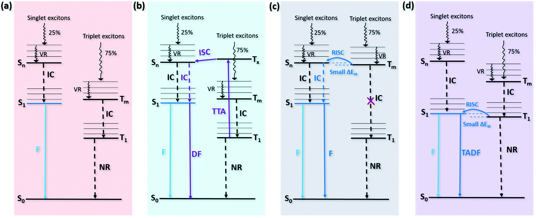 | ||
| Fig. 1 Schematic diagrams of singlet emission mechanisms for (a) conventional fluorescence. (b) Triplet–triplet annihilation (TTA), (c) hybridized local and charge-transfer (HLCT) excited state, and (d) thermally activated delayed fluorescence (TADF). | ||
![[thin space (1/6-em)]](https://www.rsc.org/images/entities/char_2009.gif) :3 as charges are injected according to the spin statistical limit.15,16 The upper limit of the internal quantum efficiency (IQE, the ratio of the number of generated photons to the number of injected charges) of OLEDs using conventional fluorescent emitters is around 25% because of the radiative decay of singlet excitons and the non-radiative decay of triplet excitons (Fig. 1a). And the maximum external quantum efficiency (EQE) of such devices can only reach roughly 5%, which can be described by the following equation:
:3 as charges are injected according to the spin statistical limit.15,16 The upper limit of the internal quantum efficiency (IQE, the ratio of the number of generated photons to the number of injected charges) of OLEDs using conventional fluorescent emitters is around 25% because of the radiative decay of singlet excitons and the non-radiative decay of triplet excitons (Fig. 1a). And the maximum external quantum efficiency (EQE) of such devices can only reach roughly 5%, which can be described by the following equation:| EQEmax = ηr × ηST × ΦPL × ηout = IQEmax × ηout |
| T1 + T1 → Tx + S0 → Sn + S0 → S1 + S0 |
| S1 + S0 → 2S0 + hν |
 | ||
| Fig. 2 The schematic energy transfer routes of the TTA process. Reproduced with permission from ref. 21. Copyright 2014 The Royal Society of Chemistry. | ||
The accumulation of triplet excitons is an essential condition for efficient TTA-OLEDs. However, the concentrated triplet excitons may result in serious efficiency roll-off. One recent work points out that the efficiency roll-off in TTA-OLEDs can be suppressed.22 They reported a highly efficient blue-emitting material, phenanthroimidazole–anthracene (PIAnCN), and obtained non-doped system-based OLED devices with a low efficiency-roll-off. By combining rigid planar π-conjugated phenanthroimidazole with cyano substituted anthracene, the expectant molecule can utilize the non-emissive triplet excitons through a triplet fusion process. The non-doped blue device exhibits a high EQE of 9.44% at 1000 cd m−2 and the efficiency remains at 8.09% even the brightness reaches 10000 cd m−2. The results imply that the quenching of triplet excitons is suppressed in such a non-doped system. For device stability, it is also necessary to suppress the quenching of triplet excitons in the TTA process so as to prolong the lifetime of TTA-OLEDs. In 2016, Hsin and co-workers found that the addition of a 10% assistant host (volume concentration) into the EML could reduce the quenching of triplet excitons and block the diffusion of triplet pairs.23 Thus, the operation lifetime (T95) of blue TTA-OLEDs was increased by 89.3% from 28 to 53 hours at an initial luminance of 2000 cd m−2. In 2017, the same group developed a commercial blue TTA-OLED structure used for mass production.24 The standard structure had a T90 lifetime of 34 hours at 2000 cd m−2 and the T50 lifetime could reach 8000 hours at 1000 cd m−2. The commercial blue TTA-OLED structure exhibited an extended operation lifetime (T90) of 550 hours at an initial luminance of 2000 cd m−2 since a new ETL material, layer structure optimization and double EML structures were adopted in the structure.
In addition to the synthesis of materials with TTA properties, changing a fluorescent material to a TTA material is also a way to pursue efficient OLEDs.25,26 This strategy requires exciplexes or sensitizers to assist the accumulation of triplet excitons in the luminescent layer.
Due to the exact demands on energy level, the design and the synthesis of an HLCT molecule are very challenging. HLCT molecules should ideally contain intercrossed local excited (LE) states (for efficient fluorescence emission) and charge transfer (CT) states (for efficient RISC), which means after the molecule is excited, orbital overlap and orbital spatial separation are satisfied at the same time. A molecule with a twisting donor unit and acceptor unit may possess such HLCT excited states. Notably, the appropriate twisting angle and the appropriate ratio of these two excited states are crucial.29 The non-linear relationship between the solvent polarity and Stokes shift, along with the single-exponential curve of PL lifetime, indicates that this type of molecule possesses HLCT states but not a mixture of LE and CT states.28,29 Different from TTA and TADF materials, neither delayed PL nor delayed EL lifetime was measured in HLCT materials. The short exciton lifetime is attributed to the faster rate of RISC (kRISC) compared to the radiative rate, which is caused by the high-lying triplet energy transfer. Meanwhile the fast RISC process from the high-lying triplet to singlet state can suppress triplet–triplet and singlet–triplet quenching caused by the accumulated triplet excitons in the device, which further reduces efficiency roll-off and increases device stability.27 But there is a lack of direct experimental evidence for the proposed hot exciton RISC process. In addition, although the HLCT emitters have shown a high ηST of 93%, the overall EQE is still limited by the low PLQY.28
In addition, Tang and co-workers reported several aggregation-induced emission-assisted hybrid local and charge transfer (AIE-HLCT) molecules, which consist of an AIE moiety and an HLCT-type core. The corresponding non-doped OLED devices exhibited a small efficiency roll-off and a maximum EQE of 7.16%.33
where kB is the Boltzmann constant and T is the temperature in centigrade. It is obvious that a small ΔEST is required for fast RISC.

The first pure organic TADF molecule (PIC-TRZ) was reported by Adachi and co-workers in 2011.41 They found that the twisted donor–acceptor structure of PIC-TRZ can lead to a reduced orbital overlap between the HOMO and LUMO. The calculated ΔEST is as low as 0.11 eV. A high EQE of 5.3% was obtained by using PIC-TRZ as an emitter while the theoretical EQE was only 2% for a conventional fluorescent emitter with a PLQY of 39%. They attributed the results to the efficient up-conversion of the RISC process. Afterward, a series of pure organic TADF emitters with both small ΔEST and high PLQY were reported by Adachi and co-workers.35 An OLED with the green TADF emitter (4CzIPN) exhibited an outstanding EQE of 19.3%, and the values were 11.2% and 8.0% for orange and sky-blue OLEDs, respectively. These results indicate that TADF is a feasible strategy for achieving high-efficiency OLEDs. Up to now, the highest EQE values of ∼38% for blue, ∼37% for green, and ∼28% for red OLEDs have been achieved by using various TADF-based emitters, which are far beyond the device efficiency of conventional fluorescent OLEDs and even comparable with phosphorescent OLEDs.38–40
However, the stability of TADF-OLEDs cannot meet the requirements of mass production, especially blue TADF devices. We summarize several blue TADF devices based on the stability reported in recent years. In 2015, the operation lifetime (T80) of blue TADF devices is only 52 hours at an initial luminance of 500 cd m−2 reported by Lee and co-workers.42 In 2016, a T50 of 770 hours at an initial luminance of 500 cd m−2 was reported by adopting a sterically shielded sky-blue TADF emitter.43 In 2017, Adachi and co-workers reported a stable blue TADF-OLED with an operation lifetime of 454 hours at an initial luminance of 1000 cd m−2 by employing an n-type material as the host.44 In 2018, Adachi and co-workers synthesized a stable sky-blue TADF emitter, namely 3Ph2CzCzBN.45 To the best of our knowledge, the device showed the longest T80 of 118 hours at an initial luminance of 1000 cd m−2. Therefore, the poor stability of blue TADF-OLEDs is still a problem to be solved.
2.2. Doublet emission
Radical-based emitters, whose emission originates from doublet excited states, have attracted more attention and obtained efficiency breakthrough in recent years.46,47 Unlike fluorescence and phosphorescence emitting molecules, radical-based emitter molecules have odd electrons and are in open-shell states due to unpaired outer orbital electrons. Fig. 3 is the spin configurations of closed-shell and open-shell molecules.46 When a closed-shell molecule (fluorescent or phosphorescent molecule) is excited, one electron will be transferred to the LUMO, and the other will remain at the HOMO. In this case, the spin quantum number obtained from these two electrons can be 0 or 1, corresponding to the singlet and triplet states respectively (Fig. 3a).48 However, the triplet excitons of pure organic fluorescent molecules can’t transit to the ground state for emission as a result of the Pauli exclusion principle.15 For an open-shell molecule, the excited state is called a doublet because the spin quantum number is 1/2. And when the only ground-state electron at the singly occupied molecular orbital (SOMO) is excited to the lowest singly unoccupied molecular orbital (SUMO), it can jump back to the SOMO without any forbidden rules (Fig. 3b). Thus the IQE of the radical emitter based on an open-shell structure is theoretically 100%. | ||
| Fig. 3 The spin configurations of (a) closed-shell molecules and (b) open-shell molecules. Reproduced with permission from ref. 46. Copyright 2015 Wiley-VCH Verlag GmbH & Co. KGaA, Weinheim. | ||
Although stable emission radicals have been reported since 2006,49–51 the first radical OLED was fabricated in 2015.46 Nonetheless, radical OLEDs got a big breakthrough in 2018.47 Ai and co-workers fabricated OLEDs using a stable radical molecule (TTM-3NCz) and obtained almost 100% IQE, as well as an excellent EQE of 27% in the deep red/near-infrared spectral range. By combining the radical TTM moiety with the donor group of 3NCz, the radical molecule can selectively control the injection of holes and electrons to the HOMO and SOMO, respectively. Doublet excitons with a small band gap are formed based on the HOMO and SOMO, therefore, the emission color is in the deep red/near-infrared spectral range. However, no stable blue light-emitting radical has been reported up to now, which limits the further development of radical OLEDs.
2.3. Triplet emission
In terms of device operation stability, the reported T95 (operational duration of the device till the luminance is decayed to 95% of the initial luminance, which is 1000 cd m−2) of green and red PhOLEDs is longer than 10000 hours.69 Nevertheless, long-lived blue PhOLEDs have not been realized since their first demonstration in 2001.70 To the best of our knowledge, the champion T80 of sky-blue PhOLEDs with a single emitting layer is only about 334 h with CIE coordinates of (0.16, 0.30).71 High energy excitons and polarons generated by exciton–exciton annihilation and exciton–polaron annihilation are considered as the main degradation mechanisms for PhOLED devices.72–74 The degradation probability of blue PhOLEDs is higher than that of red and green PhOLEDs since blue-emitting layers generate more high energy excitons and polarons through annihilation reactions, which will break the weak chemical bonds between the Ir core metal and organic ligands.75 Low abundance of precious metals and poor stability of blue devices are pushing scientists to research new solutions or provide alternatives to phosphorescent emitters.
3. Design of device structures
OLEDs typically have a multilayered device structure as shown in Fig. 4a, including an anode, hole injection layer (HIL), hole transport layer (HTL), light-emitting layer (LEL), electron transport layer (ETL), electron injection layer (EIL) and cathode. Electrons and holes are injected into the LEL from the two electrodes and then recombined on emitter molecules to emit light, while the emission color is determined by the emitter molecule. Obviously, the design and optimization of the device architecture are one of the key ways to obtaining highly efficient and stable OLEDs; thus, numerous strategies have been presented to boost the charge transport, promote the charge injection, as well as facilitate the radiative recombination.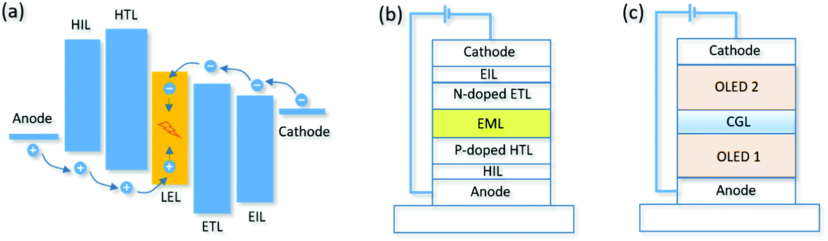 | ||
| Fig. 4 Representative device architectures of OLEDs. (a) The working mechanism of OLEDs, (b) charge injection and transport in OLEDs enhanced by p- and n-type electrical doping, and (c) tandem OLED structures with stacked emission units connected by a charge generation layer (CGL). | ||
3.1. Doping
To boost the efficiency output of OLEDs, strategies aiming at reducing the operation voltage have been proposed for enhancing the carrier conductivities of organic layers and matching the energy levels of functional layers. By introducing such a strategy, the energy loss during charge injecting and transporting processes is dramatically reduced. Molecular doping of organic layers is an effective strategy to overcome the intrinsic limitations of transport conductivity of organic layers and address the large carrier injection barriers at the organic/electrode interfaces.84,85 As the schematic architecture is shown in Fig. 4b, the device with a p-type doped HTL, an intrinsic emission layer, and an n-type doped ETL is generally regarded as an efficient OLED, which has highly reduced operating voltage at high luminance.86 To date, the representative p-type and n-type dopants used for electrical doping are transition metal oxides (TMOs) (e.g., MoO3, WO3, V2O5, ReO3, etc.) and alkali metal compounds (e.g., Cs2CO3, LiF, CsF, etc.), respectively.87–95 | ||
| Fig. 5 (a) Electrical characteristics of hole-only CBP devices (left), the energy difference between EF and HOMO edge (middle), and conductivity (right) as a function of MoO3 concentration. Reproduced with permission. Reproduced with permission from ref. 88. Copyright 2009 Elsevier. (b) Electrical characteristics of the OLED with a CsF-doped Alq3 ETL (left) and energy difference between EF and the HOMO edge (right) as a function of CsF concentration. Reproduced with permission. Reproduced with permission from ref. 93. Copyright 2013 Elsevier. | ||
Apart from the difference in electrical characteristics, the operational stability of organic devices with an n-type doped ETL is strongly affected by the doping mechanism of different alkali metal compounds.91 Without generating metallic Cs during the Cs2CO3 doping process, the diffusion of metal atoms through the ETLs into the adjacent emission layers can be suppressed, avoiding the consequential non-radiative recombination of excitons. As a comparison, the thermally evaporated CsN3 will be completely decomposed and the Cs atoms are simultaneously released in the organic ETLs, which result in the formation of non-radiative recombination centers and the quenching of the excitons, as well as degraded device performance.98 Therefore, the OLEDs using Cs2CO3 as the n-type dopant show advantages in both electrical properties and operational stability.
3.2. Tandem and multi-junction structures
OLEDs using tandem structures offer a highly attractive option for future general lighting due to the extremely high brightness and efficiency at a low driving current, along with the long operational lifetime.99,100 In a tandem OLED, vertically stacked emission units are electrically connected in series by a charge generation layer (CGL), and the brightness and current efficiency at a given current density can linearly scale with the number of emission units (Fig. 4c). Upon the application of an electric field, electrons and holes generated by the CGL would be injected into the neighboring ETL and HTL of the respective emission unit and subsequently recombine with holes injected from the anode side or electrons injected from the cathode side for light emission. Thus, the design of an efficient CGL is imperative to the high-performance electron-to-photon conversion process in tandem OLEDs.The requirements of an effective CGL mainly include high charge generation capacity, low optical absorption, low series resistance, and excellent operational stability.101 Typically, the CGLs in tandem OLEDs comprise bilayer structures, including metal/metal oxide, organic/metal oxide and organic/organic types.100–104 Following the discussion in Section 3.1., this section would focus on a representative CGL structure with an organic/metal oxide bilayer. In this CGL, TMO materials are often used adjacent to the HTL of the neighboring emission unit, while the organic layers commonly doped by n-type alkali metals or metal compounds are incorporated adjacent to the ETL of the neighboring emission unit. The functionality of MoO3-based CGL, for instance, is fully clarified, showing that the vacuum-deposited MoO3 layer is responsible for charge generation due to spontaneous electron transfer from various defect states to the conduction band via thermal diffusion.95 The external electric field induces charge separation through extraction of charge carriers into the neighboring charge transport layers. The n-doped organic layer can not only facilitate electron extraction into the neighboring ETL but also block the leakage of holes across the CGL into the HTL of the adjacent emission unit. From the perspective of long lifetime merit of tandem OLEDs, the influence of constituent materials and the operational stability of CGLs has also been illustrated. Taking different n-dopants including Mg, Cs2CO3, and CsN3 as an example, the stability of tandem devices is highly sensitive to the doping constituent materials used in the CGLs, in spite of the similar energy level barrier.105 The findings suggest that the operational stability of the n-doped layers in CGLs is the main factor responsible for device degradation due to the different doping mechanisms.
In addition to the mechanistic study, one of the most intriguing advantages of tandem OLEDs is the extremely high luminous efficiency. By employing efficient phosphorescent emitters, a triple-junction green OLED using HATCN-based CGLs exhibits a current efficiency of 256 cd A−1 at a luminance of 100 cd m−2.106 To unlock the full potential of tandem OLEDs, a phosphorescent OLED with a combination of triple emission units and a light outcoupling structure has achieved an ultrahigh current efficiency of 366 cd A−1 at 1000 cd m−2 together with a maximum EQE of 119.7%.107 Based on this strategy, microcavity-induced angle-dependent emission in tandem OLEDs can be alleviated, and the operational lifetime can be simultaneously enhanced by a factor of >10 when comparing the double junction device with the conventional device with a planar single-unit structure.108
3.3. Exciplex
Exciplexes are generated in a mixed film or an interface consisting of both a p-type donor material and an n-type acceptor material. Generally, the formation of an exciplex requires a large offset between the HOMO of the donor material and the LUMO of the acceptor material. Notably, the emission energy of the exciplex is smaller than that of each component. In recent years, exciplexes have been frequently investigated in OLEDs, since exciplexes can act as both an emitter and a host for fluorescent, TADF and phosphorescent emitters.40,109–119 Moreover, exciplex-based OLEDs exhibit prominent advantages, such as good carrier balance, low driving voltage, and high efficiency.Particularly for conventional fluorescent emitters, the exciton utilization can reach nearly 100% when exciplex hosts have TADF characteristics.114 As shown in Fig. 6a, two conditions should be satisfied for achieving high-efficiency fluorescent OLEDs. On the one hand, an efficient Förster energy transfer (FRET) process from S1 of the exciplex host to S1 of the fluorescent emitter is crucial, which requires an efficient RISC process of the exciplex host and a larger spectrum overlap between the absorption of the fluorescent dopant and the emission of the exciplex host.114,120 On the other hand, the triplet excitons formed directly on the fluorescent dopant or transferred indirectly to the fluorescent dopant should be minimized. To solve this problem, an extremely low fluorescent dopant concentration is required which can reduce the direct exciton trapping by the dopant and suppress the short-range Dexter energy transfer process from T1 of the exciplex host to T1 of the dopant. In addition, designing appropriate HOMO and LUMO of both the host and dopant can also restrain the dopant from trapping excitons.114 Therefore, full exciton utilization and high EQE can be achieved for fluorescent OLEDs by adopting an exciplex host strategy.
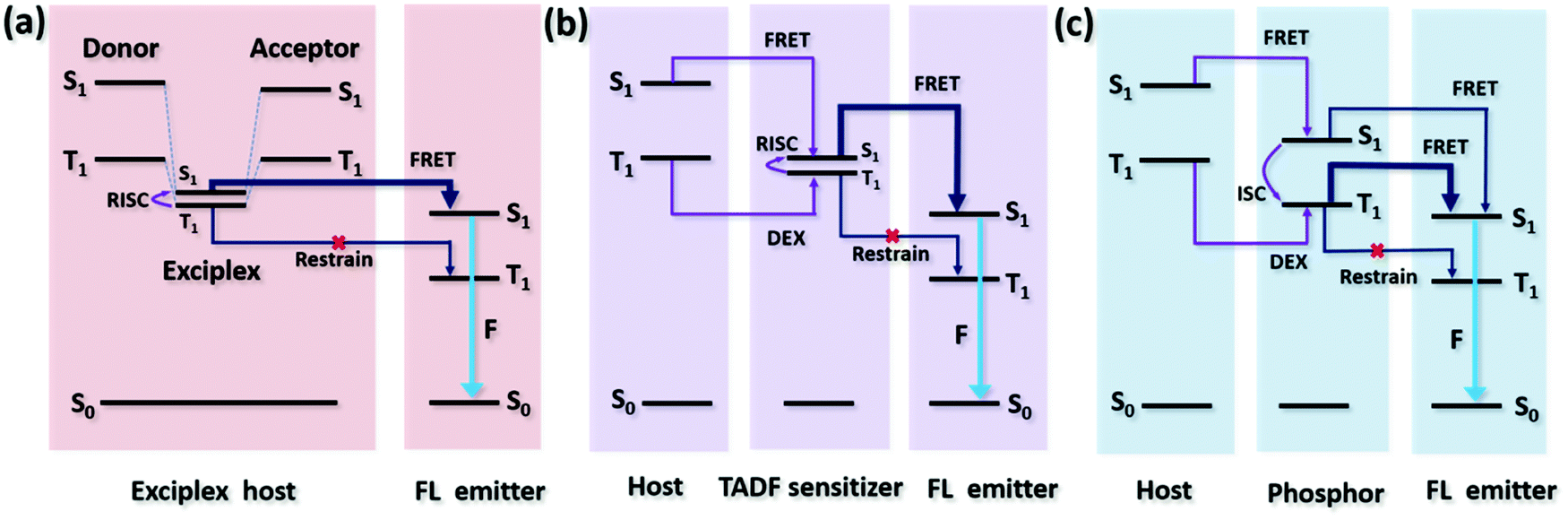 | ||
| Fig. 6 Schematic diagrams of sensitized fluorescent OLEDs. (a) Exciplex sensitized FOLEDs, (b) TADF sensitized FOLEDs and (c) phosphor sensitized FOLEDs. | ||
3.4. Sensitized fluorescence
High-EQE OLEDs can be obtained by using TADF and phosphorescent emitters. However, the poor stability of blue TADF and phosphorescent OLEDs is still an unsolved problem. Blue fluorescent OLEDs have long operational lifetime but the EQE is limited to about 5% due to low exciton utilization. Fortunately, the low exciton utilization of conventional fluorescent OLEDs can be enhanced by a sensitized approach.114,121–127Fig. 6 shows the schematic diagrams of sensitized fluorescent OLEDs; the sensitizer can be an exciplex, TADF emitter, and phosphor. In the previous section, we have discussed exciplex sensitized fluorescence OLEDs (Fig. 6a). However, blue OLEDs require a bluer emission spectrum of the exciplex. At the same time, the bluer exciplex requires a larger offset between the HOMO of the donor material and the LUMO of the acceptor material, and the emission energy of both the donor and acceptor should be larger. Therefore, this method is not suitable for blue OLEDs due to the rare blue exciplex.For TADF sensitized fluorescent OLEDs, the photophysical process and required conditions are similar to those of an exciplex. The FRET process of excitons from S1 of TADF to S1 of the fluorescent emitter is the main energy transfer channel and the Dexter energy transfer process should be restrained (Fig. 6b). In addition to the conditions mentioned in the previous section, the TADF emitter should be able to have a large doping concentration of 15 wt% to 100 wt%. By using this approach, Adachi and co-workers reported a series of high-efficiency fluorescent OLEDs with EQE from 13.4% to 18% in the full spectrum range. In particular, a sensitized orange OLED showed a longer operation time compared to a pure TADF OLED.121 Moreover, Duan and co-workers reported another approach to inhibit the short-range Dexter energy transfer by modifying traditional fluorescent dopants with electronically inert terminal-substituents. The sensitized OLED exhibited an excellent EQE of 24% and a low-efficiency roll-off by combining with an interfacial exciplex.125
Due to the strong spin–orbit coupling effect, phosphorescent materials can emit light by triplet excitons and promote the ISC process from S1 to T1. Therefore, unlike TADF sensitized fluorescent OLEDs, the energy transfer of phosphor sensitized OLEDs mainly follows the route from T1 of phosphor to S1 of the fluorescent emitter by FRET (Fig. 6c). Based on such a strategy, a high-efficiency sky-blue fluorescent OLED with a long T80 of 320 h was obtained by Lovrincic and co-workers in 2018.126 In summary, developing sensitized fluorescent OLEDs is a possible approach to obtain efficient and stable blue OLEDs.
4. Light extraction technologies
4.1. Light extraction losses
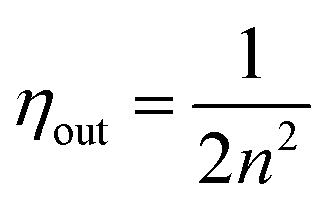
As mentioned above, significant progress has been made in improving the internal quantum efficiency (IQE) to a high level of ∼100% with the full use of both singlet and triplet states. Unfortunately, most of the emitted photons are trapped within the device due to the optical confinement and internal reflection by the mismatched refractive index of the multilayer structure.128,129 The fraction of the extracted light to the air ηout can be estimated based on ray optics according to Snell's law:Here n depicts the effective refractive index of the organic layer stack with respect to the air space. Thus, the calculated extraction of light to the free space is only about 17%.130,131 To gain further insight into optical loss channels, a more accurate treatment according to wave optical methods has been extensively investigated. As depicted in Fig. 7, an excited molecule can couple into different optical modes in such a flat stack structure. A significant portion of emitted photons are confined within the substrate (substrate mode, ∼23%),132 guided within the organic layers and transparent anode (waveguide mode, ∼15%)130,133 and dissipated at the organic–cathode interface (SPP mode, ∼40%),134,135 resulting in only ∼18% of energy flow being radiated outside the device as useful light. Thereby, the low-outcoupling efficiency limits highly efficient OLEDs. Accordingly, various advanced light out-coupling approaches have been extensively explored to recover the wasted photons for practical lighting and display applications in recent years, as will be discussed in detail.
 | ||
| Fig. 7 Schematic illustration of various kinds of optical loss channels in conventional flat architectures. | ||
4.2. Microscale structures
To date, various methods have been proposed to enhance the light extraction for OLEDs. For this purpose, particular structures are desirable to effectively decrease the incident angles at the interfaces, and thus avoid the total internal reflection of emitted light. From the point of view of ray optics, microscale structures constructed on device substrates can efficiently suppress the substrate mode loss. Möller and Forrest incorporated a poly-dimethyl-siloxane (PDMS) microlens array (MLA) film with a diameter of 10 μm onto a glass substrate as a light extraction film, which was produced by photolithographic techniques and a mold transfer process.136 The EQE of OLEDs with MLAs was enhanced by a factor of at least 1.5, and no color changes of the emission were observed. Later, Helander and co-workers reported a double layer green OLED with a maximum PE of 230 lm W−1 by combining a chlorinated ITO cathode and the MLAs.137 Yang and co-workers demonstrated an enhancement of the light extraction efficiency by incorporating three differently sized MLAs onto a glass substrate, which were fabricated with the employment of a roll-to-roll mold transfer process on polycarbonate (PC) films (Fig. 8a).138 Compared to the flat device, the light extraction enhancement ratios of devices with various MLAs were 1.52, 1.60, and 1.36 for D50, D50-20, and D50-10 (50 μm in diameter, referred to as D50, and 50 μm in diameter and 20 μm in transverse diameter, referred to as D50-20) in the normal direction, respectively. Similarly, a negligible color shift for OLEDs with the MLA film was observed in this device configuration. Thomschke and co-workers used a thick optical cavity with a refractive index matched microlens foil as an integrating element on top-emitting WOLEDs, yielding a 4-fold increase of spectral enhancement and a record high CRI of 93 for top-emitting WOLEDs (Fig. 8b).139 Theoretical and experimental investigations demonstrated the light out-coupling ability and the integrating ability of the microlens foils, which mix the optical modes to a broadband spectrum.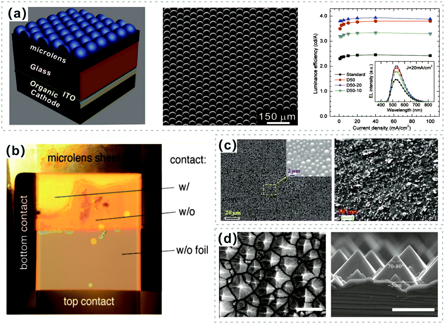 | ||
| Fig. 8 (a) (left) An OLED attached with MLAs on a glass substrate as a light extraction film, (middle) the 45° tilted view of the SEM image of MLAs with a hemispherical shape, and (right) luminance efficiency as a function of current density inserted with EL spectra of devices with and without MLAs. Reproduced with permission from ref. 138. Copyright 2010 American Institute of Physics. (b) Photography of a top-emission OLED that is only partially covered with a MLA film. Reproduced with permission from ref. 139. Copyright 2011 American Chemical Society. (c) Top-view and cross-section SEM images of a microscale sphere-based outcoupling layer. Reproduced with permission from ref. 140. Copyright 2014 Royal Society of Chemistry. (d) Top-view and cross-section SEM images of micro-pyramids of a PVA film. Reproduced with permission from ref. 141. Copyright 2005 Elsevier B.V. | ||
In addition, the introduced random-distributed microscale structures can also efficiently release the trapped photons in OLEDs. Liu and co-workers developed a flexible light extraction film, which consists of a polyethylene naphthalate (PEN) substrate and randomly distributed SiO2 spheres (refractive index of ∼1.5, an average particle size of 1.5 μm) in a SU-8 matrix (Fig. 8c).140 These embedded spheres can efficiently scatter and redirect the emitted light, thus leading to the efficiency improvement of the OLED devices. As a consequence, the fabricated flexible WOLED on the PEN substrate with a thin encapsulation film and a light extraction film exhibited a lifetime of 5.2 h at an initial luminance of 1000 cd m−2 and the maximum power efficiency exceeded 100 lm W−1 with negligible CIE variation. Except for commonly used MLAs and sphere particles, micro-pyramid structures were also investigated. Zhu and co-workers duplicated the microscale pyramid-based texture from a monocrystalline silicon surface to a polyvinyl alcohol (PVA) film using a printing process and applied it to the surface of OLEDs with the spires of pyramids facing the emitter (Fig. 8d).141 It was observed that this stratagem could effectively enhance light escape, while the CE and EQE got enhancement ratios of 37.3% and 36.6%, respectively, at a current density of 100 mA cm−2 without inducing any side effects. To sum up, the conventional substrate-mode light loss in OLEDs can be effectively weakened by means of microscale structure light extraction schemes.
4.3. Nanoscale structures
Another way of guiding the trapped light to air is the use of nanostructures based on the theory of wave optics, i.e. one-dimensional (1D) nanograting, random nanostructures, and nanoscale particles. A few representative structures will be discussed in this section.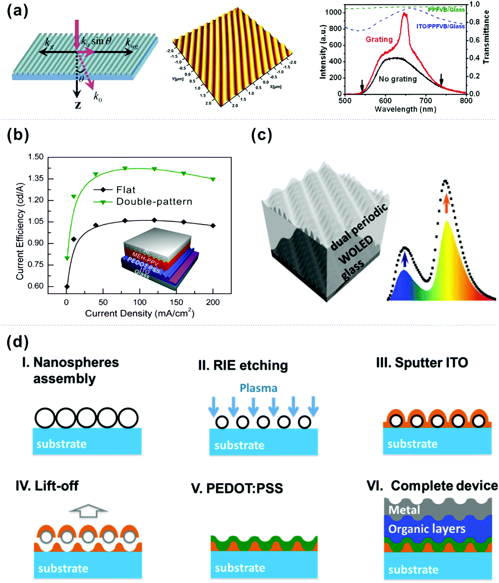 | ||
| Fig. 9 (a) (right) Schematic illustration of Bragg diffraction of waveguide light, (middle) AFM image of nanostructured azobenzene polymer, and (right) EL spectra within ±18° from the device with flat and nanostructured CYTOP layers. Reproduced with permission from ref. 146. Copyright 2008 American Institute of Physics. (b) The current efficiency of flat and double-patterned PLEDs. Reproduced with permission from ref. 147. Copyright 2014 American Chemical Society. (c) Schematic of the broadband light extraction by using dual-periodic grating. Reproduced with permission from ref. 150. Copyright 2013 Wiley-VCH Verlag GmbH & Co. KGaA, Weinheim. (d) Schematic fabrication steps of the ITO nanomesh OLED. Reproduced with permission from ref. 151. Copyright 2015 Wiley-VCH Verlag GmbH & Co. KGaA, Weinheim. | ||
Sun and co-workers illustrated broadband excitation and outcoupling of the trapped photons within the WOLEDs by introducing a two-dimensional (2D) grating with dual-periodic corrugation into the devices (Fig. 9c).150 This dedicatedly designed structure consisting of two sets of corrugations with different periods that can broaden the light was directly amenable to extracting light from the WOLEDs based on two complementary color strategies of blue and orange emission. As a consequence, a 48% enhancement of EQE was obtained compared to that of the conventional planar devices. Wu and co-workers reported a novel internal extraction structure toward high OLED efficiency by the formation of an ITO nanomesh and its filling of high-conductivity PEDOT:PSS.151 As depicted in Fig. 9d, such a structure can be readily fabricated by facile nanosphere lithography (of ITO) and spin-coating (of PEDOT:PSS), by which the EQE of OLEDs is enhanced by a factor of 41%. Considering the different refractive indices of ITO (n = 1.9–2.1) and PEDOT:PSS (n = 1.5), as well as the incomplete planarization of the ITO nanomesh, they suggested that such a significant enhancement of OLED efficiency originated from the synergetic effect of photonic crystals and surface corrugation. Therefore, employing the periodic nanograting/mesh in OLEDs has the potential to fabricate high-performance devices for commercial applications of lighting and displays.
000 cd m−2, without introducing angular or wavelength-dependent emission. Hence, aperiodic nanostructured OLEDs have the advantage of a broad distribution in periodicity and random directionality, allowing the modes guided in all azimuthal directions to be extracted over the entire emission wavelength range.
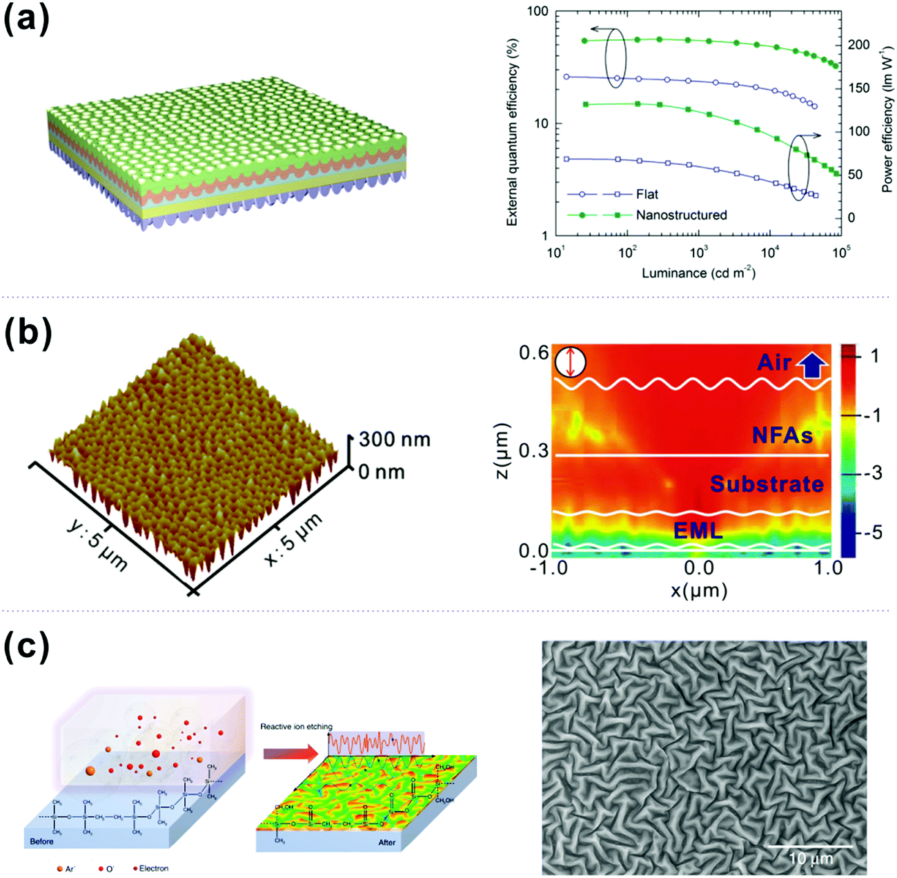 | ||
| Fig. 10 (a) Schematic of WOLEDs, in which both sides of the ITO glass substrate are patterned with MENs, along with EQE and PE as a function of luminance for the corresponding devices. Reproduced with permission from ref. 156. 2014 Wiley-VCH Verlag GmbH & Co. KGaA, Weinheim. (b) AFM images of patterned inverted MEN UV-resin on the glass surface, and calculated electric field distributions at 520 nm with a single perpendicular-oriented dipole located in the middle of the emission layer for the corrugated device. Reproduced with permission from ref. 157. 2015 Wiley-VCH Verlag GmbH & Co. KGaA, Weinheim. (c) Schematic illustrations of RIE-induced nanostructures and relevant SEM images. Reproduced with permission from ref. 158. Copyright 2019 Macmillan Publishers Limited. | ||
In addition, many studies concerning OLEDs utilizing nanoparticles (NPs) have been performed to enhance light escape. Yang et al. have demonstrated SPP-enhanced OLEDs by introducing silver NPs.159 As shown in Fig. 11a, Gu et al. reported a ∼123% enhancement of current efficiency (with a current density of 20 mA cm−2) by introducing platinum–cobalt (Pt3Co) alloy nanoparticles into devices.160 Grover and co-workers have proposed a light extracting method of incorporating a crystallized 4,7-diphenyl-1,10-phenanthroline (BPhen) film as a scattering layer at the backside of an ITO coated glass substrate.161 In Lee and co-worker's research, a 200% enhancement of PE has been achieved by using corrugated PEDOT:PSS cross-linked PS NPs as the HTL, which simultaneously reduces the optical loss and alleviate degradation of devices (Fig. 11b).162 Kim and co-workers reported performance enhancement of devices by utilizing a poly(4-butylphenyl-diphenyl-amine) (poly-TPD):dodecanethiol functionalized Au (DDT-Au) nanocomposite layer (Fig. 11c).163 Later, they observed that the enhanced EL intensity for the device with a nanocomposite layer was strongly related to the effective energy transfer between the radiated light and the LSPR excited by the DDT-Au NPs (Fig. 11d).164 Recently, a novel nanocomposite substrate consisting of a silver nanowire-based electrode, a high-index polymer layer, and a light-scattering layer has been demonstrated by Pei and co-workers (Fig. 11e).165 The high-index polymer (n = 1.7) was employed to improve the refractive index matching of the substrate and the organic layers (n = 1.7–1.8). The composite light scattering layer, comprising an acrylate admixed with high-index barium strontium titanate nanoparticles, is designed to extract waveguide-mode and substrate-mode light. Based on these versatile substrates, efficient white OLEDs with a PE of 107 lm W−1 and an EQE of 49% at 1000 cd m−2 have been subsequently fabricated. The influence of refractive indices of various components in OLEDs on light extraction will be discussed in the next section.
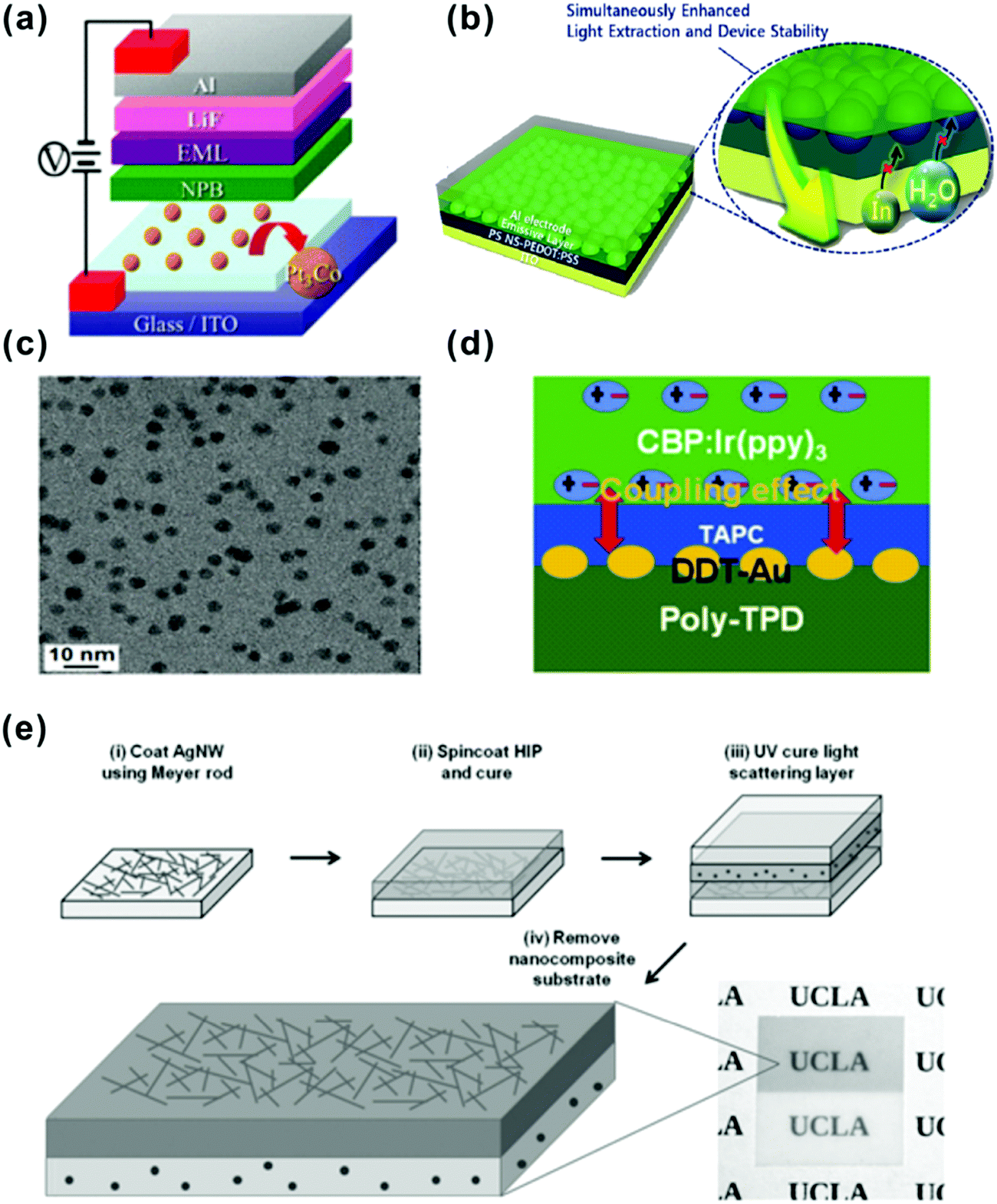 | ||
| Fig. 11 (a) Schematic device structure of an OLED incorporating Pt3Co ANPs on an ITO anode. Reproduced with permission from ref. 160. Copyright 2013 Royal Society of Chemistry. (b) Device structure with polystyrene (PS) nanospheres embedded in PEDOT:PSS films. Reproduced with permission from ref. 162. 2014 Wiley-VCH Verlag GmbH & Co. KGaA, Weinheim. (c) The TEM image of the poly-TPD:DDT-Au nanocomposite film. Reproduced with permission from ref. 163. Copyright 2015 Optical Society of America. (d) Device structure with a DDT-Au layer. Reproduced with permission from ref. 164. Copyright 2016 Elsevier B. V. (e) Fabrication process for a freestanding nanocomposite substrate containing silver nanowires embedded in the high-index polymer (HIP) layer and barium strontium titanate (BST) nanoparticles embedded in the light-scattering layer. Reproduced with permission from ref. 165. Copyright 2017 Wiley-VCH Verlag GmbH & Co. KGaA, Weinheim. | ||
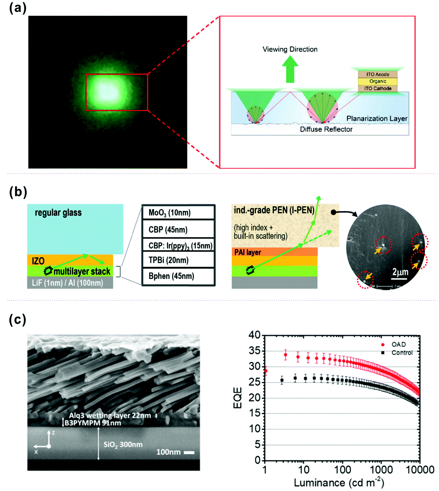 | ||
| Fig. 12 (a) Schematic illustration of the OLED on a diffuse reflector. Reproduced with permission from ref. 167. Copyright 2018 American Chemical Society. (b) Schematic diagrams of OLED structures on regular glass substrates (left) and on industrial-grade PEN (I-PEN) substrates (right). Reproduced with permission from the ref. 168. Copyright 2015 Wiley-VCH Verlag GmbH & Co. KGaA, Weinheim. (c) Cross-sectional SEM image of ∼600 nm of Alq3 deposited at 80° on top of 90 nm B3PYMPM deposited at 0° on top of 300 nm of SiO2 and EQE values of various OLEDs. Reproduced with permission from ref. 169. Copyright 2018 American Chemical Society. | ||
4.4. Multiscale structures
Recently, multiscale hierarchical structures have attracted much attention and inspired highly efficient light management approaches.170–173 As displayed in Fig. 13a, Zhou and co-workers fabricated multiscale micro-nano nested structures featuring a microlens and microtriangle array with built-in nanohole structures (MTNs) by combining the mask photolithography and controllable thermal reflow process.174 As a result, the device with MTNs constructed on glass substrates exhibited reduced reflection of 7.1% over the entire visible wavelength range, which is 3.5% lower than the bare substrate. The resulting CE and EQE were 1.60 and 1.63 times that of a flat architecture. Most recently, inspired by the multiscale structure of the firefly's cuticle, Jeong and co-workers developed a new method to fabricate this hierarchical ultrastructure using geometry-guided resist reflow, replica molding, and PDMS oxidation.175 These newly developed hierarchical structures were composed of longitudinal nanostructures and asymmetric microstructures (Fig. 13b), which can efficiently extract the photons confined in the OLED due to total internal reflection. The introduction of hierarchical structures leads to a 60% increase in the EQE and an illumination angle 16% wider than that of the flat device. As displayed in Fig. 13c, a glass-fabric reinforced siloxane hybrid (GFRH) substrate has been demonstrated as a facile substrate of OLEDs for extracting light trapped in substrate mode.176 In order to enhance light scattering inside the substrate, the refractive index of the siloxane hybrid was rationally modified to maximize the scattering of light at the interface of the matrix and the glass fabric, resulting in a film with high optical transmittance and haze. As a consequence, a high-performance OLED was successfully fabricated on the film and exhibited a 74% enhancement of EQE owing to the outstanding optical properties of the GFRH film. These newly emerging multiscale structures will set a new paradigm for light extraction engineering for commercial lighting applications.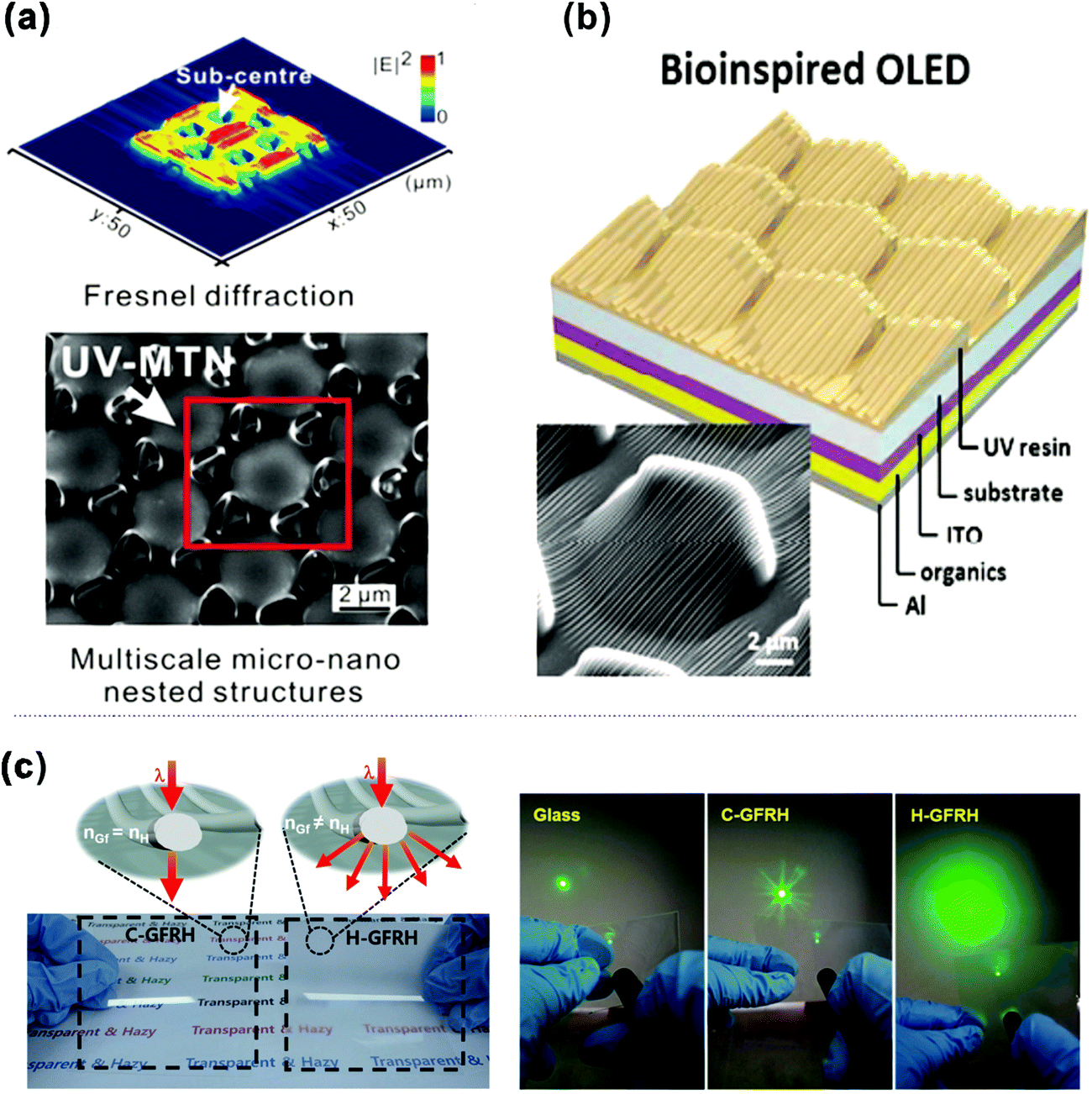 | ||
| Fig. 13 (a) (top) Calculated normalized intensity distribution of the Fresnel diffraction image for the pre-designed mask. (bottom) SEM image of micro-nano nested structures featuring a microlens and micro triangle array with built-in nanohole structures. Reproduced with permission from ref. 174. Copyright 2015 American Chemical Society. (b) The device structure of the bio-inspired OLED and the SEM image of the multiscale structures mimicking the hierarchical structures of a firefly lantern. Reproduced with permission from ref. 175. Copyright 2016 American Chemical Society. (c) Schematic illustration of the fabrication procedure for Ag-grid embedded GFRH films and light scattering by the refractive index contrast of the glass fiber and the hybrimer. The Ag grid was prepared by the gravure-offset printing method. Reproduced with permission from ref. 176. Copyright 2018 Wiley-VCH Verlag GmbH & Co. KGaA, Weinheim. | ||
4.5. Orientation of the molecular dipoles
The orientation of emitting dipoles has been demonstrated to be one of the most important properties of emitters influencing the efficiency of OLEDs. Particularly, horizontally oriented emitting dipoles in OLEDs lead to reduced light losses from surface plasmon modes and waveguide modes, hence increasing the outcoupling efficiency of OLEDs. In 2009, Adachi and co-workers demonstrated some molecular design guidelines for highly horizontally oriented materials by assessing optical properties of typical organic materials.177 They observed the fact that horizontal molecular orientation occurs on various underlying layers, implying the versatility of the horizontal orientation for various applications. Subsequently, Yokoyama and co-workers have systematically reviewed several factors of molecular orientation in vacuum deposited amorphous films of various OLED materials.178 The effect of the horizontal orientation on the light extraction of small-molecule OLEDs is schematically depicted in Fig. 14a. Since the photons were emitted mainly in the direction vertical to the transition dipole moment, the horizontal orientation was preferable for high light extraction efficiency. Frischeisen et al. presented an experimental method to straightforwardly determine dipole orientation in guest–host systems and found that light extraction was increased by around 45% when the majority of dipoles were horizontally orientated.179 It was observed that the typical green emitter of Ir(ppy)2(acac) exhibited nearly 19% higher EQE than its Ir(ppy)3 counterpart. This feature is directly attributed to the completely isotropic behavior of Ir(ppy)3 and 77% horizontally oriented aligned dipoles of Ir(ppy)2(acac).180 By using the same emitter, Lu et al. reported a high-efficiency green phosphorescent OLED adopting both the low-index ITO-free electrode and the preferentially horizontal dipole emitter of Ir(ppy)2(acac).181 The highest EQE of this proposed device at that time reached up to 64% with an MLA light extraction film (Fig. 14b). Though Ir-based complexes were reported having a horizontal orientation to improve light outcoupling, the internal mechanism had not been fully uncovered until Kim and co-workers’ report. They found that the substituents at the para-position of the pyridine in the main ligands of Ir-based complexes play a vital role in changing the orientation of Ir-based complexes.182 They concluded that horizontal emitting orientation is highly possible if Ir-based complexes are elongated by substituting aliphatic or aromatic functional moieties at the para-position of the pyridine in the main ligands. By using this scheme, stacked Ir-based complexes with orientation parallel to the film surface are formed (Fig. 14c). They benefit from the elongated and planar substituents with high electrostatic potential which enlarges the interacting surface region between the Ir-based complex and host molecules. Apart from Ir-based phosphorescent emitters, TADF-based OLEDs have also been reported showing elevated efficiencies based on horizontally orientated emitting dipoles. For instance, Lee and co-workers demonstrated that a near-perfect (100%) horizontal orientation of the TADF dipole moment can be induced by using triscarbazole donors (Fig. 14d).183 Furthermore, a triscarbazole-based emitting system possesses high PL quantum yield, which is due to the uniform distribution of the electron density in the HOMO of the donor. As a consequence, a high EQE of over 30% was obtained without any other light-extraction method. Until now, orientation engineering of emitting dipoles has attracted more and more attention for its simple and cost-effective characteristics.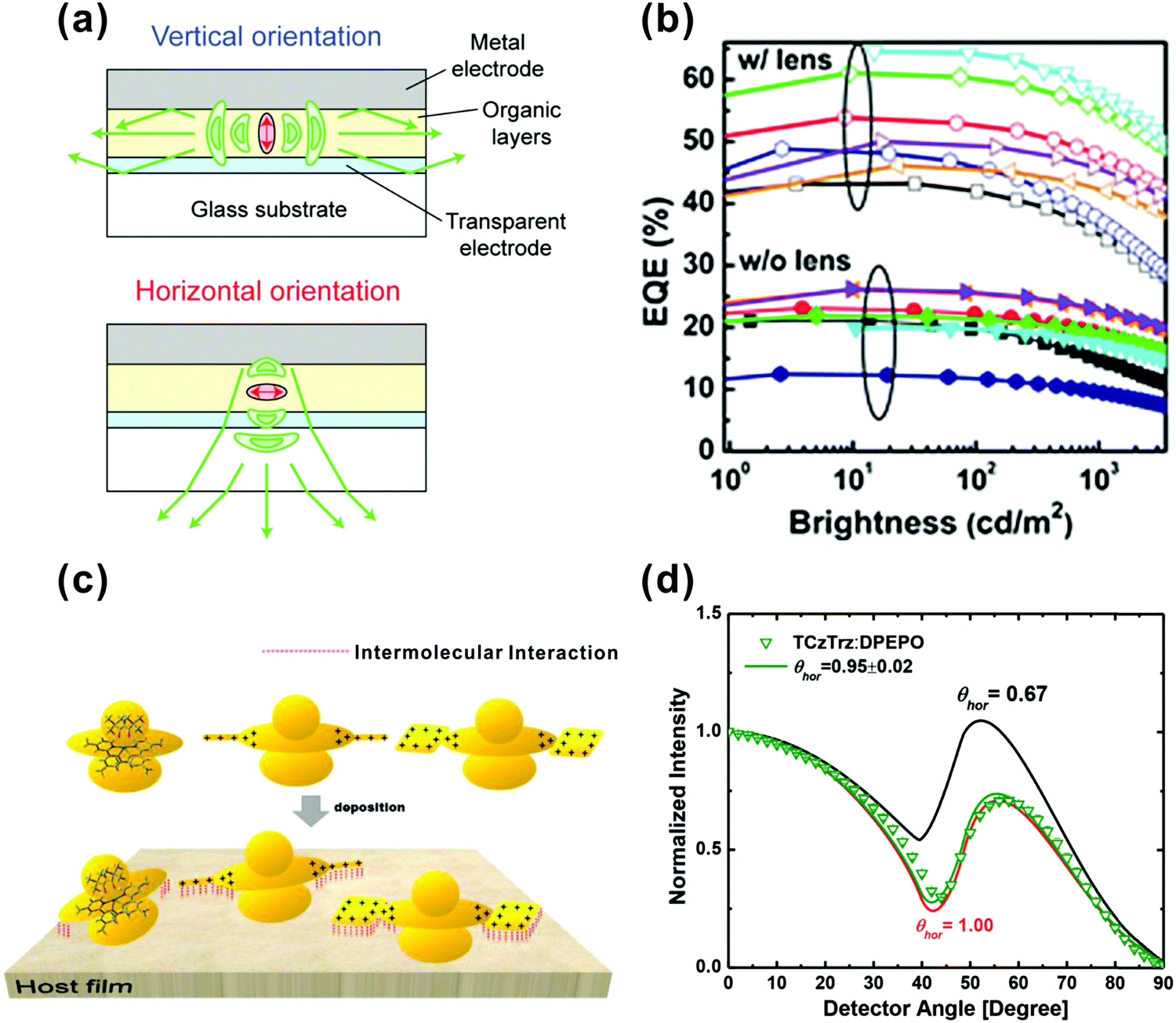 | ||
| Fig. 14 (a) Schematic of the enhancement of outcoupling efficiency of OLEDs by the horizontal orientation of the transition dipole moment of emitting molecules. Reproduced with permission from ref. 178. Copyright 2011 the Royal Society of Chemistry. (b) EQE as a function of the brightness of all Ir(ppy)2(acac) devices with and without MLAs. Reproduced with permission from ref. 181. 2016 Wiley-VCH Verlag GmbH & Co. KGaA, Weinheim. (c) Schematic of molecular orientation and intermolecular interaction of Ir complexes on a host film under vacuum deposition. Reproduced with permission from ref. 182. Copyright 2016 American Chemical Society. (d) Measured horizontal transition dipole moment ratios of TCzTrz (data points) obtained using angle-dependent PL data and calculated by optical simulation (lines). Reproduced with permission from ref. 183. Copyright 2018 Wiley-VCH Verlag GmbH & Co. KGaA, Weinheim. | ||
5. Flexible and stretchable configurations
5.1. Flexible OLEDs
Because of the compatibility with curvilinear and soft materials, mechanically flexible OLEDs are an emerging technology for flexible intelligent electronics with applications in bendable smartphones, curved displays, and flexible solid-state lighting devices.184,185 To fabricate high-performance flexible OLEDs, the key issue is to attain efficient flexible transparent conductive electrodes (TCEs) with excellent electrical, optical and mechanical properties. It is known that the most commonly used TCE of ITO cannot meet the requirements of flexible OLED technology due to several drawbacks including brittleness, material scarcity, and a low-throughput deposition process.186,187 Among all the alternative flexible TCEs, four types have very lately attracted great interest and shown promising progress for highly power-efficient flexible OLEDs. | ||
| Fig. 15 (a) Schematic of the fabrication procedure of the Ag fiber electrodes and OLEDs. Reproduced with permission from ref. 195. Copyright 2017 Wiley-VCH Verlag GmbH & Co. KGaA, Weinheim. (b) Scalable step-by-step composite electrode fabrication process. Reproduced with permission from ref. 196. Copyright 2013 Wiley-VCH Verlag GmbH & Co. KGaA, Weinheim. (c) The schematic diagram of an OLED prepared on the nanocomposite substrate and the optical mechanism for improving the out-coupling efficiency by means of periodic wrinkles. Reproduced with permission from ref. 197. Copyright 2018 Wiley-VCH Verlag GmbH & Co. KGaA, Weinheim. (d) Schematic illustration of the fabrication process for white flexible OLEDs, including the spin coating of AgNWs, the patterning of a sol–gel-derived ZnO layer, the spin coating of a PEDOT:PSS layer, and the subsequent deposition of organic layers. Reproduced with permission from ref. 198. Copyright 2019 Wiley-VCH Verlag GmbH & Co. KGaA, Weinheim. | ||
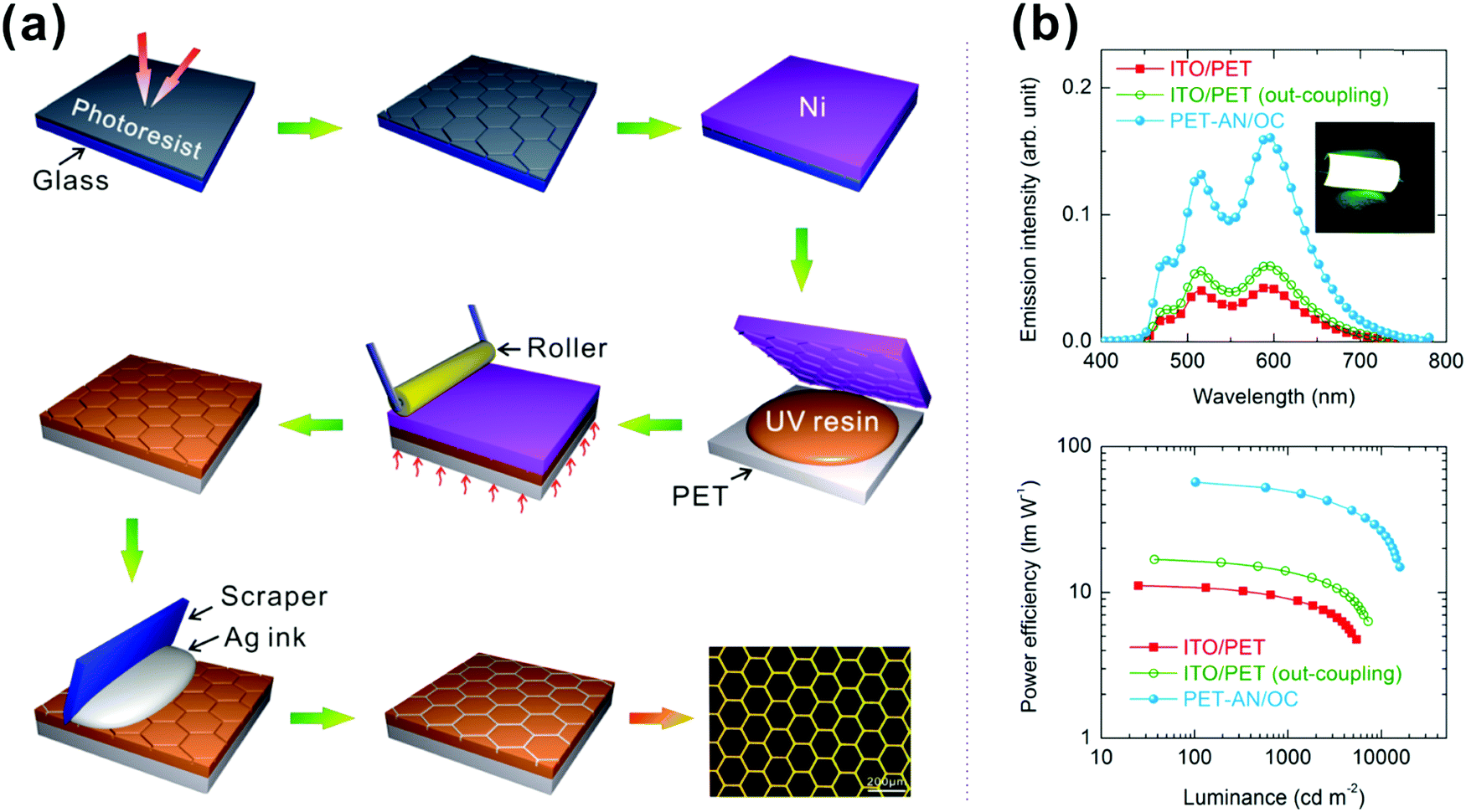 | ||
| Fig. 16 (a) Schematic illustration of the fabrication steps of an embedded Ag network on a PET substrate, including photolithography, electroforming, UV nanoimprinting lithography, plasma treating, silver-paste scratching, etc. Reproduced with permission from ref. 201. Copyright 2014 American Chemical Society. (b) EL spectra of various white FOLEDs at the same current density in the normal direction and power efficiency as a function of luminance. Reproduced with permission from ref. 202. Copyright 2015 American Chemical Society. | ||
000 cd m−2.204 Similarly, to alleviate the cavity issue induced by the flat metal thin film, an effective nanostructured metal/dielectric composite electrode in the form of MoO3/Ca/Ag/MoO3 was proposed for microcavity-free flexible OLEDs (Fig. 17a and b).205,206 In these devices, the quasi-random nanostructures for broadband and angle-independent light manipulation were integrated with an ultrathin Ca-doped Ag alloy film for electrical, optical and mechanical superiority. The fabricated large-area flexible white OLEDs yielded remarkably improved device performance, exhibiting a maximum power efficiency of 112.4 lm W−1.
 | ||
| Fig. 17 (a) Schematic illustration of flexible OLEDs using a nanostructured composite electrode and the AFM profile of imprinted UV-resin layer with quasi-random nanostructures. Reproduced with permission from ref. 205. Copyright 2016 Optical Society of America. (b) Flexible OLED structure with a nanopatterned metal-dielectric electrode on a plastic substrate and EQE values as a function of luminance. Reproduced with permission from ref. 206. Copyright 2015 American Chemical Society. | ||
000 cd m−2 with CRI of 85. Regardless of these previous electronic and electrical modifications, the photonic role of the graphene electrodes in OLEDs has recently been investigated with a synergetic interplay of high-index TiO2 layers and low-index hole injecting layers as depicted in Fig. 18b. The sandwiched graphene electrode enabled a light out-coupling enhancement through enhancing micro-cavity resonances and suppressing SPP, which further result in a maximum EQE of 33.8% and PE of 155.8 lm W−1 for flexible green OLEDs.209
 | ||
| Fig. 18 (a) Energy level diagram of the single-layer graphene (SLG) anode/PEDOT:PSS/MoO3/CBP structure. Reproduced with permission from ref. 208. Copyright 2013 Macmillan Publishers Limited. (b) Schematic device structure of the proposed OLEDs and electromagnetic field intensity distribution (dashed lines) of the OLEDs under study for their respective first-order cavity design. Reproduced with permission from ref. 209. Copyright 2016 Macmillan Publishers Limited. | ||
5.2. Stretchable OLEDs
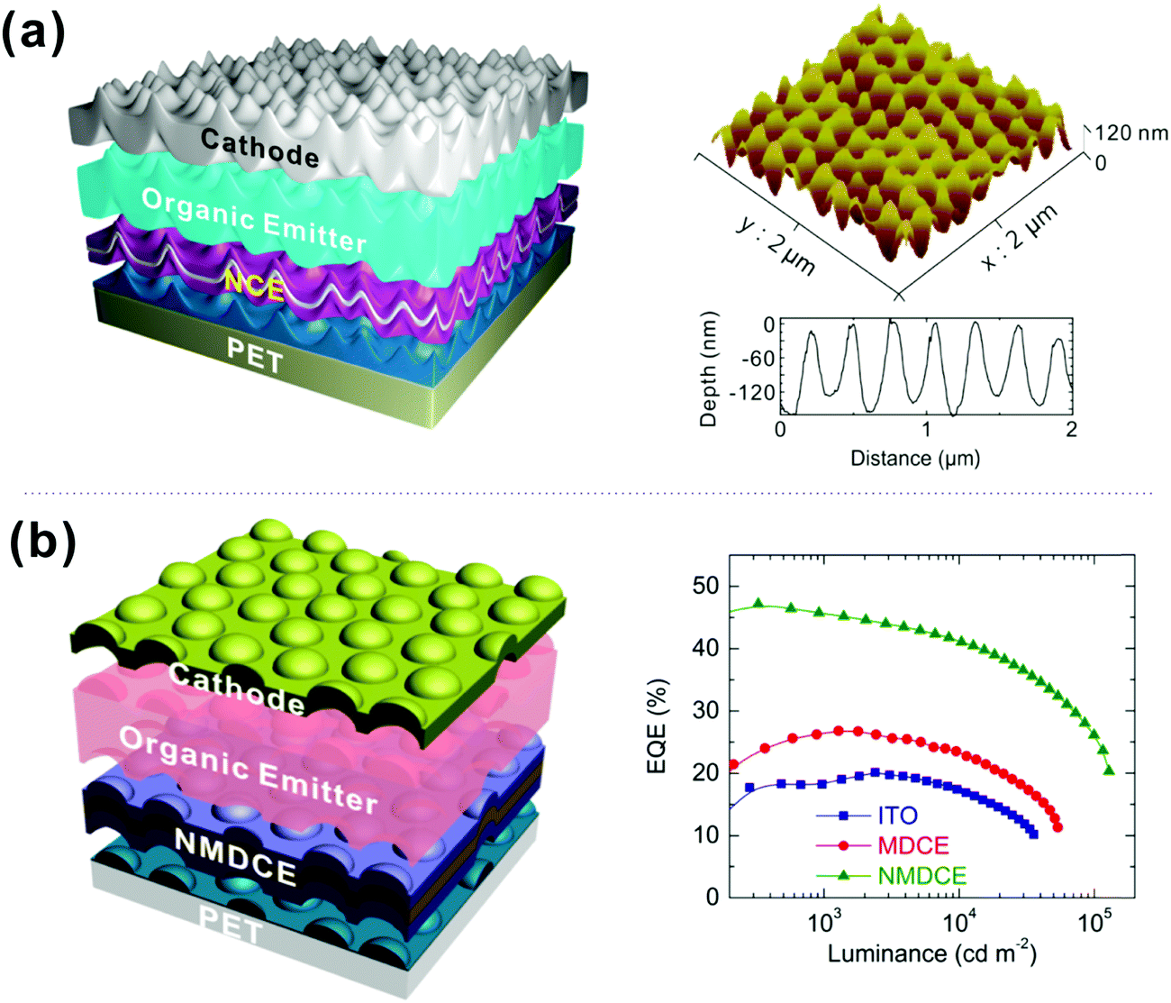
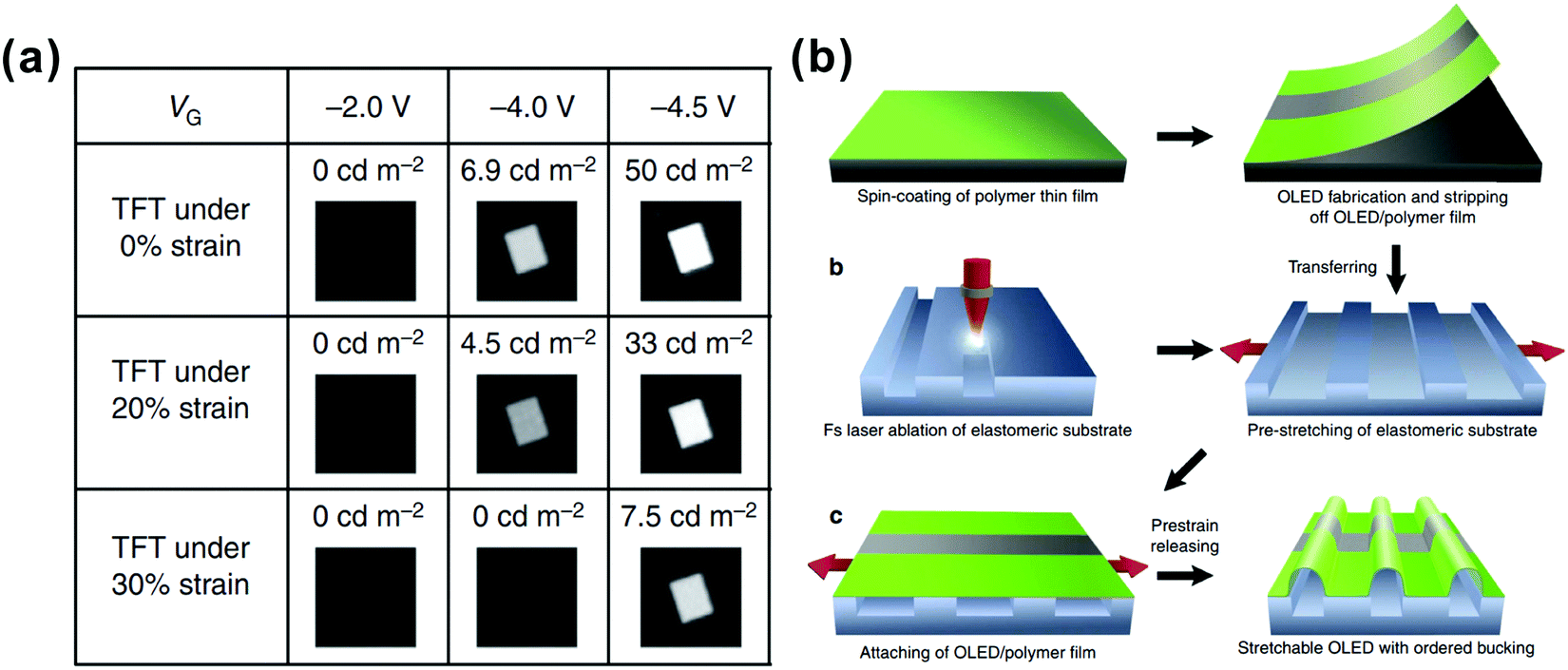
Stretchable light emission devices are becoming increasingly significant in the fast-growing fields of wearable display and lighting systems, as well as biomedical and health-monitoring technologies.210,211 The unique requirement of these devices imposed in this field is the high flexibility and stretchability, which aims at undergoing mechanical deformation at various degrees. To fabricate operational stretchable OLEDs, flexible TCEs and substrates are supposed to be prepared in advance. The intrinsically malleable polymer-based light-emitting systems are of great benefit for realizing stretchable OLED devices. For example, Sekitani and co-workers have demonstrated printable elastic conductors comprising single-walled carbon nanotubes (SWNTs) uniformly dispersed in a fluorinated rubber.212 They fabricated a rubber-like stretchable active-matrix display integrated with printed elastic conductors, organic transistors, and organic light-emitting diodes, which can be stretched by 30–50% and spread over a hemisphere without any mechanical or electrical damage. Interestingly, stretchable thin-film transistors (TFTs) have been reported by a solution printing process using a silver nanowire (AgNW)-PU acrylate (PUA) composite as the stretchable transparent electrode. Such facile TFTs were employed to drive OLEDs by controlling “on” and “off”, by which stretchable lighting was realized213 (Fig. 19a). Recently, a new efficient prototype of stretchable OLEDs has been released through a laser-programmable buckling process, showing a high efficiency of 70 cd A−1 under 70% strain and mechanical robustness with small performance fluctuations over 15000 stretch–release cycles214 (Fig. 19b). Another type of intrinsically stretchable OLED device is the utilization of polymer light-emitting electrochemical cells. In this elastomeric device, a pair of transparent composite electrodes using a thin percolation network of silver nanowires or carbon nanotubes are inlaid in the surface layer of the rubbery substrate, which allows the device to be collapsible and operable under repeated continuous stretching cycles.215 Significant progress has been made in producing fully stretchable OLEDs for practical applications in bendable and wearable electronics, especially in lighting and display applications where high luminescent performance and mechanical stability are both required. As two important roles in the architecture engineering of OLEDs, light outcoupling techniques and flexible TCEs can be synergistically employed to fabricate efficient flexible OLEDs. It is noteworthy that from the aspect of the light-extraction effect, most flexible TCEs can also be treated as an excellent light outcoupling scheme for their light-scattering or refractive-index engineering contributions.
 | ||
| Fig. 19 (a) Luminance of an OLED driven by stretchable TFT under different inputs. Reproduced with permission from ref. 213. Copyright 2015 Macmillan Publishers Limited. (b) Schematic illustration of the fabrication process of stretchable OLEDs, including OLED preparation, substrate preparation, and stretchable OLED assembly by attaching. Reproduced with permission from ref. 214. Copyright 2016 Macmillan Publishers Limited. | ||
6. Fabrication technologies
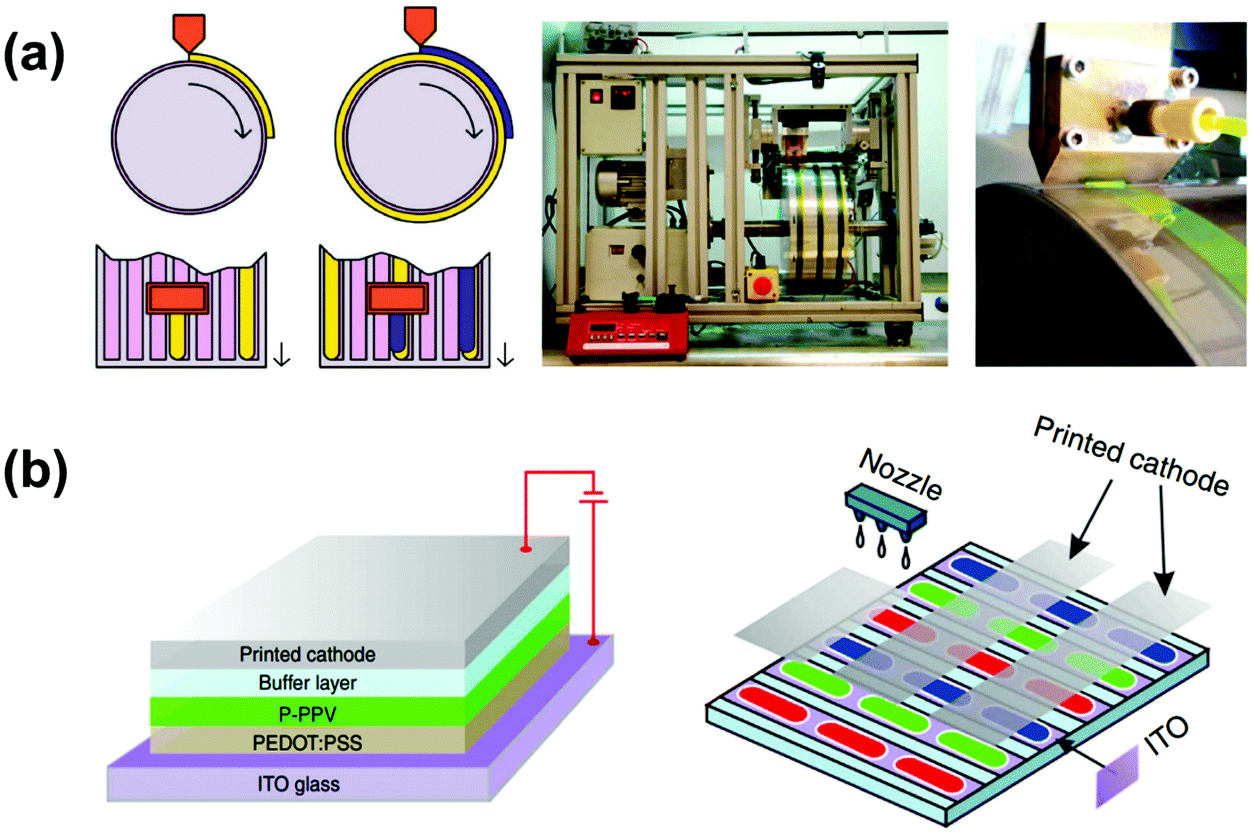
OLEDs can be typically fabricated in two ways, namely, the physical vapor deposition technique and solution techniques including screen printing, spin-coating, inkjet printing, photolithographic process, and micro-contact printing, etc. Physical vapor deposition technology is widely used in depositing various active layers for fabricating small molecular OLEDs. This technique is applicable only for low molecular weight materials and the thermally stable lanthanide complexes. The main advantage of this technique is that it is directly amenable to complicated multilayer device structures without any serious technical problems. However, this technology is time-consuming, energy-consuming, and of limited use for large-area devices especially emerging flexible and stretchable devices.216Compared with the vapor deposition technology, the solution process techniques are simpler and less expensive, which offer several advantages such as large-area coverage, low power consumption, and much easier device manufacture. Friend et al. developed the first polymer light-emitting diode (PLED) by a spin-coating technique using a conjugated polymer poly(phenylene-vinylene) (PPV) in 1990.2 The next year, Braun and Heeger introduced the insoluble polymer, PPV, to the soluble polymer, poly(2-methoxy-5-(2′-ethyl-hexoxy)-1,4-phenylene-vinylene) (MEH-PPV), and fabricated PLEDs by the spin-coating method.217 Hebner and co-workers fabricated OLEDs with low turn-on voltages using polyvinylcarbazole (PVK) luminescence films deposited by ink-jet printing technology.218 Müller et al. reported pixelated three-color OLED matrix displays by a spin-coating process using emitter polymers with photoresist properties.219 As depicted in Fig. 20a, Sandström et al. reported an all-solution-based flexible light-emitting electrochemical cell using a slot-die roll-coating apparatus.220 The entire manufacturing procedure was carried out in air, which is directly compatible with high-speed and low-cost roll-to-roll fabrication although the constituent processed needed to be further optimized. Lately, Zheng et al. produced a 1.5-inch all-solution-processed PLED display using ink-jet conducting nanoparticles as the cathode which is deposited on a multifunctional buffer layer (Fig. 20b).216
 | ||
| Fig. 20 (a) Schematic view of the slot-die coating of the active layer and the anode on top of the flexible cathode-coated substrate; photograph of the roll coater and close-up photograph of the slot-die head during coating of an active layer stripe. Reproduced with permission from ref. 220. Copyright 2012 Macmillan Publishers Limited. (b) The device structure of the all-solution-processed PLED single device with the printed nanoparticle cathode and schematic illustration of the display structure of the full-color display. Reproduced with permission from ref. 216. Copyright 2013 Macmillan Publishers Limited. | ||
Additionally, solution processing technology is not only used for those based on PLEDs but also extensively investigated for the fabrication of small molecule-based OLEDs (SMOLEDs). Cai et al. reported spin-coated electrophosphorescent SMOLEDs with 4,2′-bis(9-carbazolyl)-biphenyl (CBP) doped with the green-emitting tris[2-(p-tolyl)pyridine] iridium(III) (Ir(mppy)3), and obtained a high peak PE of 60 lm W−1.221 This high-performance device implied that the spin-coating technique was an attractive and alternative route to the fabrication of multi-component devices. Zhao et al. synthesized a series of small molecular hole transport materials, which were realized by connecting the flexible moieties of butadiene bridged triphenylamine (BTPA) to N,N,N′,N′-tetraphenyl-[1,1′-biphenyl]-4,4′-diamine (TPD) (TPD(BTPA))n (n = 1, 2, 3, 4). The spin-coated OLEDs with TPD(BTPA)4 exhibited a comparable CE to devices fabricated by physical vapor deposition.222 In 2015, Kido and co-workers reported tandem green emission OLEDs and WOLEDs comprising two phosphorescent light-emitting units using the spin-coating method.223 Here, the ZnO nanoparticle/polyethlyeneimine-ethoxylated (PEIE) bilayer acted as the electron injection layers and the PEDOT:PSS was adopted as the interconnecting conductive layer. The spin-coated green tandem-OLED and WOLED yielded a high CE of 94 cd A−1 and 69 cd A−1, respectively, at a current density of 5000 cd m−2.
Recently, some attractive progress has been made in transferring TADF technology to a solution processable platform, which offers a possible path to fabricating low-cost, large-area, high-performance TADF-OLEDs. In 2015, Nikolaenko et al. reported the first efficient spin-coated TADF-OLEDs with an EQE of 10% based on the formation of a single polymeric material containing intermonomer charge transfer state (namely intermonomer TADF) emitters.224 Chen et al. reported a non-doped and solution-processed blue OLED based on B-oTC, and obtained an EQE of 19.1% along with a CIE of (0.15, 0.26).225 Wada et al. realized a highly efficient solution-processable blue TADF-OLED with an EQE of 22.1% and CIE of (0.15, 0.19) by using their design strategy.226 Cho and co-workers synthesized blue TADF emitters and fabricated efficient blue TADF OLEDs using the spin-coating technique.227 This device exhibited a high EQE of 20% with color coordinates of (0.16, 0.26), which was comparable to that of a vapor deposited blue TADF device. Albrecht et al. reported an effective route for the synthesis of carbazole dendrons with a triphenyl-s-triazine core.228 It was the first solution-processable and non-doped high-molecular-weight TADF material. Verma et al. demonstrated TADF-OLEDs with an IQE of 13.9% by the inkjet-printing technique under atmospheric conditions based on the so-called NHetPHOS copper complex family.229 Most recently, Adachi's group reported a high efficiency, spin-coated TADF-OLED with an EQE of 9.3% using a new class of π-conjugated polymers (namely pCzBP and pAcBP).230 In short, there are three types of emitters that can be used in solution-processable OLEDs, including small molecules, dendrimers, and polymers. Compared with the conventional thermal evaporation technique, solution-processable methods are gaining more and more attention for their low cost and simple process. It is expected that the quality of solution-processed OLEDs may be greatly improved through the synergistic modification of the fluid properties and printing techniques for organic solutions, which are thus probable to win a place in the future lighting and display markets.
7. Solid-state lighting (SSL) and display technologies
7.1. Development and progress of WOLEDs for SSL
Solid-state lighting (SSL), defined as the use of semiconductor electroluminescence to produce visible light for illumination, will make greener buildings that use less electricity, making life less dependent on fossil fuels. In the coming decade, SSL will become key to constructing low-cost and high-performance buildings that consume less energy and produce fewer greenhouse gas emissions than their counterparts. SSL sources based on WOLEDs have gained considerable attention of academic and industrial research communities as the next-generation lighting sources since the first report of a WOLED by Kido in 1994.231 Compared to existing light sources, such as incandescent light bulbs, fluorescent lamps, and inorganic LEDs, WOLEDs offer extreme light-weight, flexibility, light uniformity, glare-free display and thin profiles that are more comfortable for human perception.232–235 There are several key performance factors of WOLEDs for SSL, including efficiency, lifetime, and color quality. In the previous sections, we have discussed some strategies for obtaining OLEDs with high efficiency and long lifetime. As for color quality, two critical sub-factors are required for achieving a high-quality WOLED, including a limited CIE chromaticity coordinate close to the black-body curve with a correlated color temperature (CCT) between 2500 K and 6500 K, and a CRI above 80.3 Over the past two decades, great advances of WOLEDs in lighting technology have been made.000 h at 1000 cd m−2 with the utilization of a high-refractive-index microlens array.240 In addition, a white Ph-OLED with a PE of 105 lm W−1 without light extraction structure was reported by Fung et al. in 2017.117 In 2018, Kim et al. reported a high-efficiency WOLED with an excellent EQE of 78% and a PE of 164 lm W−1 by employing both internal (random vacuum nanohole array) and external light extraction structures (half-spherical lens).241 In the same year, Tang et al. reported a transparent flexible WOLED with a nano-patterned metal-dielectric composite electrode, and the WOLED exhibited an excellent EQE of 72.4% and an extremely high PE of 168.5 lm W−1 with a CRI of above 84.242
In the industry field, considerable efforts have been devoted so far to realizing high-performance WOLEDs for SSL applications. In 2005, GE Global Research fabricated a 2 ft × 2 ft white OLED panel with a PE of 15 lm W−1, a CCT of 4400 K and a CRI of 88 (Fig. 21a).243 In 2008, Research Institute of Organic Electronics in Japan demonstrated 14 cm × 14 cm prototyping WOLED panels with a PE of 20 lm W−1 (@5000 cd m−2).244 In 2010, Panasonic company reported high-quality WOLED panels with PE > 30 lm W−1, CRI > 90 and half-decay lifetime >40000 h (@1000 cd m−2). Moreover, the lifetime was improved to 80000 h by using an efficient heat radiation thin encapsulation structure.245 In the same year, Universal Display Corporation developed two 15 cm × 15 cm OLED lighting panels: Panel 1 and Panel 2. Panel 1 exhibited a PE of 58 lm W−1, CRI of 86 and CCT of 2790 (see Fig. 21b), while Panel 2 showed a PE of 50 lm W−1, CRI of 87, CCT of 3055 and LT70 of 10000 h.246 In 2018, OLED Works company used thin glass substrates to fabricate a bendable OLED lighting panel, and the bending radius of the panel can be decreased to 10 cm as shown in Fig. 21c.247 In addition to the plane lighting panel, the kirigami-based 3D OLED lighting has also been reported by Kim et al. in 2018.248
 | ||
| Fig. 21 Commerical and potential applications of WOLEDs for solid-state lighting. (a–c) WOLED lighting panels developed by commercial companies. Reproduced with permission from ref. 243, 246 and 247. Copyright 2005–2018 SID. (d) OLED tulip illumination. Reproduced with permission from ref. 249. Copyright 2017 John Wiley & Sons, Inc. | ||
OLED lighting panels have many advantages, such as extreme lightweight, thin profile, glare-free display, flexibility and light uniformity, allowing various attractive designs and innovative applications. For example, beautiful tulip lighting flowers can be fabricated by using flexible plane OLEDs as light sources, while conventional point, linear and circular light sources could not make it possible (Fig. 21d).249 In addition, Philips fabricated an interactive OLED mirror, which can be applied in the hallway or next to the cloakroom.250 Moreover, WOLEDs can be used as portable lighting, which is ideal for use during plant ‘shutdowns’ for maintenance and installation requirements. Alkilu developed a portable OLED light panel, which is about 10 × 10 cm in size and has a color temperature of 3000 K. More importantly, this apparatus has a Li-polymer battery that can last for more than 30 hours.251 Japan-based Stanley Electric developed an OLED tail light prototype and aimed to commercialize such a tail lamp by 2020.252 Therefore, it is doubtless that high-performance novelty OLED products with low material loss and higher added values will boost the potential lucrative niche markets of SSL.
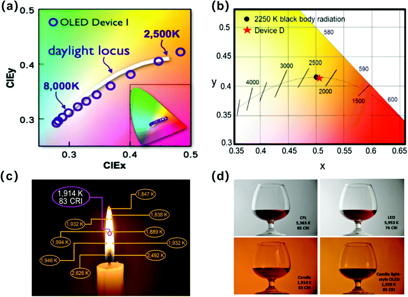 | ||
| Fig. 22 Optimized physiologically friendly light sources. (a) Chromaticity and color-temperature characteristics of the sunlight-style OLED. Reproduced with permission from ref. 255. Copyright 2009 American Institute of Physics. (b) CIE chromaticity coordinates of WOLEDs with the solar spectrum. Reproduced with permission from ref. 257. Copyright 2016 Elsevier. (c) Candle shows different color temperatures at different flame positions. Reproduced with permission. Reproduced with permission from ref. 259. Copyright 2013 Wiley-VCH Verlag GmbH & Co. KGaA, Weinheim. (d) Lighting color temperature effect on the photographic results of a wine containing glass illuminated by different light sources. Reproduced with permission. Reproduced with permission from ref. 259. Copyright 2013 Wiley-VCH Verlag GmbH & Co. KGaA, Weinheim. | ||
7.2. Development and progress of OLED displays
OLED displays have appeared on the flat-panel display market to compete against conventional cathode-ray tubes (CRTs) and liquid-crystal displays (LCDs) since the mid-1980s.260,261 The main feature is that OLED displays can perfectly control the variations of brightness and generate color within subpixels of red, green, and blue colors inside a panel, whereas LCD displays are transmissive devices which can’t fully block the backlight. Compared with an LCD display, an OLED display has a thinner body, higher color contrast, faster response speed, potentially lower power consumption and even lower cost since the latter does not require a backlight.262 And the OLED can achieve a flexible display, which is difficult for the LCD. However, there are still some urgent problems to be solved in OLEDs. For example, the relatively faster decay of commercial blue emitters than green and red emitters during the operation led to a color deviation, especially in large size display screens. Although some strategies were proposed to compensate for the deficiency of blue emission, developing commercial blue emitters with high efficiency and good stability is still necessary.263,264 For now, at least in small-size display screens, such as smartwatches and smartphones, OLEDs have obvious advantages over LCDs.Nowadays, OLED displays have already been extensively used in Audio/Video players, digital cameras, wearable devices, mobile phones, laptops, and OLED TV displays. For example, in 2010, Sony Corporation fabricated an Audio player with a 2.8-inch OLED display and a resolution of 240 × 240 pixels.265 In 2016, Sony also introduced a new type of digital camera with 3K OLED viewfinder.266 At the same time, various digital camera manufacturers (e.g., Panasonic, Fujifilm, Nikon) have introduced new high-quality products with OLED displays. In addition, the worldwide wearable device market will continue to grow in the future. Various stylish wearable devices have begun to adopt OLED displays for superior color quality, such as fitness bands and head-mounted displays. For instance, the Apple Watch Series 2 as the 2nd-generation smartwatch has adopted an OLED display with 272 × 340 pixels. In particular, the Apple Watch Series 5 as all-weather retina OLED display adopted low-temperature polycrystalline oxide (LTPO) backplane technology.267 Simultaneously, OLED displays can be used in virtual reality (VR) displays for 3D viewing because of the high resolution and high degree of comfort. The OLED technology is also used in many smartphones today, for instance, the iPhone X has adopted a 5.8′′ 1125 × 2436 AMOLED display.268 For OLED TVs, since 2010, LG developed a 15-inch 1366 × 768 HD TV and has been constantly developing large-size high resolution OLED TVs that can compete with high-end LED/LCD TVs (Fig. 23).263,269–273 By 2015 LG developed 55′′, 65′′, 77′′ flexible 4K ultra high definition (UHD) TVs.271–273 In 2016, LG display demonstrated a 55′′ full high definition (FHD) transparent OLED TV.263 Moreover, OLED display technology is also widely adopted in computer products (e.g., Dell Computer Corporation, Hewlett-Packard Development Company), digital recording binoculars, and portable video magnifiers. Alienware developed and commercialized the latest gaming laptop with 13-inch 2560 × 1440 OLED displays.274 This laptop is similar to the previous product (LCD Alienware 13 R2), just with an OLED instead of the LCD display. Similarly, in some other commercial products, OLED displays have gradually been adopted. For instance, Sony introduced a binocular-camera that stands alone in the digital binocular market – it records 2D and 3D video in full high definition and features a 5-inch touch OLED display.275 If this trend continues, we might conclude that the OLED display technology would become mainstream in a couple of years.
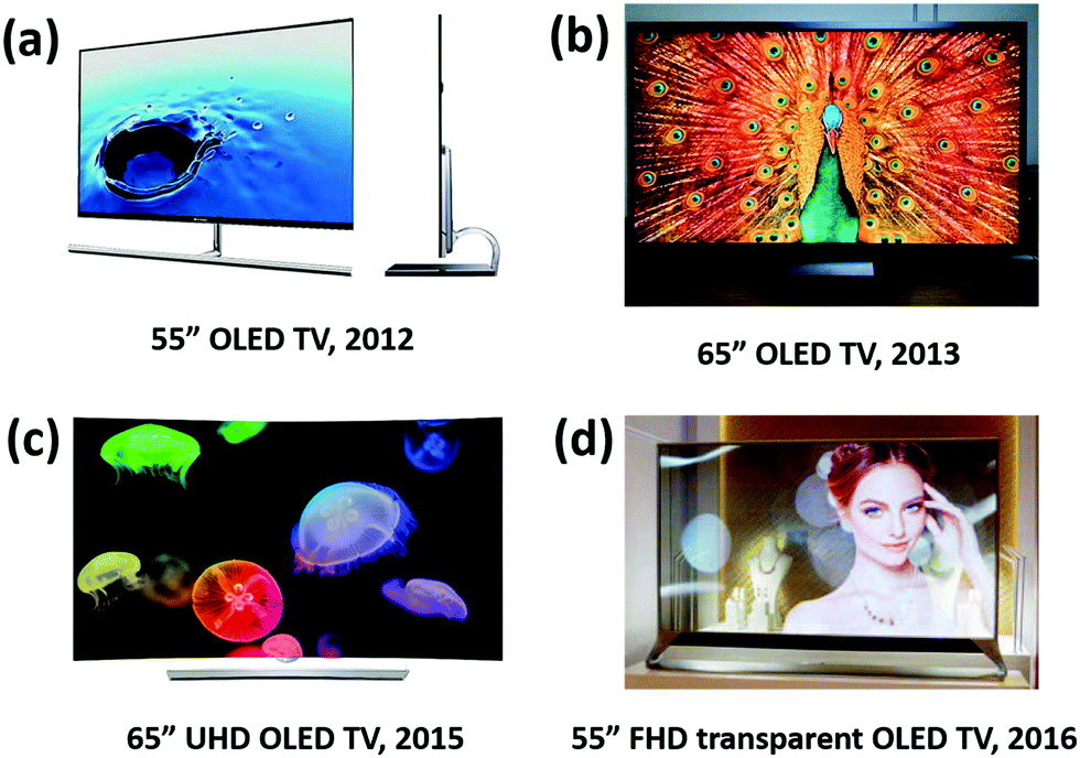 | ||
| Fig. 23 The OLED TVs developed by LG displays. Reproduced with permission from ref. 263, 269, 270 and 272. Copyright 2012–2017 SID. | ||
8. Summary and perspectives
In this paper, we have systematically reviewed recent advances in OLED materials, device architectures, light extraction approaches, fabrication techniques, as well as breakthroughs in organic SSL and displays. Different materials and the corresponding emission principle have been firstly summarized. Some advanced mechanisms, such as TADF and TTA, might unlock the theoretical limit of OLED devices. A variety of light extraction schemes with the implementation of micro-nano structures have been demonstrated to contribute to release the trapped photons of the devices. The rapid development techniques of flexible and stretchable OLEDs provide attractive prospects for future flexible or foldable OLED-based applications. Meanwhile, solution-processed fabrication approaches, such as spin-coating and ink-jet printing, could efficiently reduce the manufacturing cost. These scientific efforts have improved the performance of OLEDs and accelerated their commercial application.However, it is noteworthy that major technological challenges need to be overcome for OLEDs to become a success in the future. First, affordability might be a critical challenging goal, although OLEDs have already been commercialized as organic SSL and displays in numerous consumer electronics. The manufacturing costs have to be reduced significantly so that they can compete with the existing technologies and gradually dominate the display and SSL market. An alternative way to reduce the cost is through the roll-to-roll (reel-to-reel) fabrication technologies with high throughput.
Second, the significant progress in inorganic light-emitting diodes (LEDs) as backlight sources of liquid crystal displays (LCDs) with a dramatic decrease in power consumption is weakening the competitiveness of OLEDs over LCDs. Although advanced optical light extraction engineering has made attractive progress, an important challenge for these techniques is to directly transfer the structures over a large area at a very low cost.
Thirdly, recently emerged colloidal quantum dot LEDs (QLEDs) have attracted great interest both in scientific and industry domains. QLEDs generally exhibit superior color purity compared with OLEDs, although QLED technologies are not yet mature enough to be used in SSL and displays. However, combined with blue LED-based backlight solutions, QLEDs have been successfully incorporated into today's advanced LCD displays, which might bring unexpected challenges for OLEDs' future applications.
Last, one of the disadvantages of OLEDs is their individual lifetime. The lifetime of blue devices is relatively shorter than other colored devices. The reported T95 of the red and green devices has already exceeded 10000 hours at 1000 cd m−2.69 TADF offers many possibilities for stable blue OLEDs, but this technology is not mature enough to provide answers yet. It remains an urgent task to prevent aging of the devices.
Although the challenges facing OLEDs are significant, rapid progress in the development of OLEDs in recent years provides significant confidence in this promising technology for future lighting and displays. We believe that scientific research in OLEDs is vibrant and expanding, and OLEDs will enter our everyday life with an exciting new form-factor in the near future.
Conflicts of interest
There are no conflicts to declare.Acknowledgements
This work was financially supported by the National Natural Science Foundation of China (No. 61520106012, 61905171, 61722404, 51873138, 91633301), the National Key R&D Program of China (No. 2016YFB0401002, 2016YFB0400700), the Natural Science Foundation of Jiangsu Province of China (BK20190815), the 333 Program (No. BRA2019061), and the Collaborative Innovation Center of Suzhou Nano Science & Technology.References
- C. W. Tang and S. A. VanSlyke, Appl. Phys. Lett., 1987, 51, 913 CrossRef CAS.
- J. H. Burroughes, D. D. C. Bradley, A. R. Brown, R. N. Marks, K. Mackay, R. H. Friend, P. L. Burns and A. B. Holmes, Nature, 1990, 347, 539 CrossRef CAS.
- B. W. D’Andrade and S. R. Forrest, Adv. Mater., 2004, 16, 1585 CrossRef.
- G. Schwartz, S. Reineke, T. C. Rosenow, K. Walzer and K. Leo, Adv. Funct. Mater., 2009, 19, 1319 CrossRef CAS.
- J. Lee, H. F. Chen, T. Batagoda, C. Coburn, P. I. Djurovich, M. E. Thompson and S. R. Forrest, Nat. Mater., 2015, 15, 92 CrossRef PubMed.
- C. Y. Kuei, W. L. Tsai, B. Tong, M. Jiao, W. K. Lee, Y. Chi and P. T. Chou, Adv. Mater., 2016, 28, 2795 CrossRef CAS PubMed.
- Y. J. Cho, K. S. Yook and J. Y. Lee, Adv. Mater., 2014, 26, 4050 CrossRef CAS PubMed.
- M. Kim, S. K. Jeon, S. H. Hwang and J. Y. Lee, Adv. Mater., 2015, 27, 2515 CrossRef CAS PubMed.
- L. S. Hung and C. H. Chen, Mater. Sci. Eng., R, 2002, 39, 143 CrossRef.
- C. Lee and J. J. Kim, Small, 2013, 9, 3858 CrossRef CAS PubMed.
- T. Yamasaki, K. Sumioka and T. Tsutsui, Appl. Phys. Lett., 2000, 76, 1243 CrossRef CAS.
- K. Meerholz and D. C. Müller, Adv. Funct. Mater., 2001, 11, 251 CrossRef CAS.
- D. Zhang, K. Ryu, X. Liu, E. Polikarpov, J. Ly, M. E. Tompson and C. Zhou, Nano Lett., 2006, 6, 1880 CrossRef CAS PubMed.
- D. S. Hecht, L. Hu and G. Irvin, Adv. Mater., 2011, 23, 1482 CrossRef CAS PubMed.
- M. Pope and C. E. Swenberg, Electronic processes in organic crystals and polymers, Oxford University Press on Demand, 1999 Search PubMed.
- M. A. Baldo, D. F. O’brien and S. R. Forrest, Phys. Rev. B: Condens. Matter Mater. Phys., 1999, 60, 14422 CrossRef CAS.
- T. Arakane, M. Funahashi, H. Kuma, K. Fukuoka, K. Ikeda, H. Yamamoto, F. Moriwaki and C. Hosokawa, SID Symp. Dig. Tech. Pap., 2006, 37, 37 CrossRef.
- C.-J. Chiang, A. Kimyonok, M. K. Etherington, G. C. Griffiths, V. Jankus, F. Turksoy and A. P. Monkman, Adv. Funct. Mater., 2013, 23, 739 CrossRef CAS.
- D. Y. Kondakov, Philos. Trans. R. Soc., A, 2015, 373, 2014032 Search PubMed.
- Y. Luo and H. Aziz, Adv. Funct. Mater., 2010, 20, 1285 CrossRef CAS.
- J. Zhou, P. Chen, X. Wang, Y. Wang, Y. Wang, F. Li, M. Yang, Y. Huang, J. Yu and Z. Lu, Chem. Commun., 2014, 50, 7586 RSC.
- X. Tang, Q. Bai, T. Shan, J. Li, Y. Gao, F. Liu, H. Liu, Q. Peng, B. Yang, F. Li and P. Lu, Adv. Funct. Mater., 2018, 28, 1705813 CrossRef.
- M. H. Hsin, C. Y. Lee, Y. C. Chen, P. Y. Chen, Y. H. Chen, H. H. Lu, Y. H. Lin, B. Y. Lin, M. Z. Lee, T. L. Chiu, C. F. Lin and J. H. Lee, SID Symp. Dig. Tech. Pap., 2016, 47, 1727 CrossRef CAS.
- B. Y. Lin, M. Z. Lee, P. C. Tseng, J. H. Lee, T. L. Chiu, C. F. Lin, J. Hsieh and S. Chen, SID Symp. Dig. Tech. Pap., 2017, 48, 1928 CrossRef CAS.
- B. Y. Lin, C. J. Easley, C. H. Chen, P. C. Tseng, M. Z. Lee, P. H. Sher, J. K. Wang, T. L. Chiu, C. F. Lin, C. J. Bardeen and J. H. Lee, ACS Appl. Mater. Interfaces, 2017, 9, 10963 CrossRef CAS PubMed.
- C. H. Chen, N. T. Tierce, M. K. Leung, T. L. Chiu, C. F. Lin, C. J. Bardeen and J. H. Lee, Adv. Mater., 2018, 30, e1804850 CrossRef PubMed.
- D. Hu, L. Yao, B. Yang and Y. Ma, Philos. Trans. R. Soc., A, 2015, 373, 20140318 CrossRef PubMed.
- W. Li, Y. Pan, R. Xiao, Q. Peng, S. Zhang, D. Ma, F. Li, F. Shen, Y. Wang, B. Yang and Y. Ma, Adv. Funct. Mater., 2014, 24, 1609 CrossRef CAS.
- W. Li, D. Liu, F. Shen, D. Ma, Z. Wang, T. Feng, Y. Xu, B. Yang and Y. Ma, Adv. Funct. Mater., 2012, 22, 2797 CrossRef CAS.
- L. Yao, S. Zhang, R. Wang, W. Li, F. Shen, B. Yang and Y. Ma, Angew. Chem., Int. Ed., 2014, 53, 2119 CrossRef CAS PubMed.
- X. Tang, Q. Bai, Q. Peng, Y. Gao, J. Li, Y. Liu, L. Yao, P. Lu, B. Yang and Y. Ma, Chem. Mater., 2015, 27, 7050 CrossRef CAS.
- B. Liu, Z.-W. Yu, D. He, Z.-L. Zhu, J. Zheng, Y.-D. Yu, W.-F. Xie, Q.-X. Tong and C.-S. Lee, J. Mater. Chem. C, 2017, 5, 5402 RSC.
- H. Zhang, J. Zeng, W. Luo, H. Wu, C. Zeng, K. Zhang, W. Feng, Z. Wang, Z. Zhao and B. Z. Tang, J. Mater. Chem. C, 2019, 7, 6359 RSC.
- M. Kasha, Discuss. Faraday Soc., 1950, 9, 14, 10.1039/DF9500900014.
- H. Uoyama, K. Goushi, K. Shizu, H. Nomura and C. Adachi, Nature, 2012, 492, 234 CrossRef CAS PubMed.
- S. Y. Lee, T. Yasuda, Y. S. Yang, Q. Zhang and C. Adachi, Angew. Chem., Int. Ed., 2014, 53, 6402 CrossRef CAS PubMed.
- Y. Shu and B. G. Levine, J. Chem. Phys., 2015, 142, 104104 CrossRef PubMed.
- D. H. Ahn, S. W. Kim, H. Lee, I. J. Ko, D. Karthik, J. Y. Lee and J. H. Kwon, Nat. Photonics, 2019, 13, 540 CrossRef CAS.
- T.-L. Wu, M.-J. Huang, C.-C. Lin, P.-Y. Huang, T.-Y. Chou, R.-W. Chen-Cheng, H.-W. Lin, R.-S. Liu and C.-H. Cheng, Nat. Photonics, 2018, 12, 235 CrossRef CAS.
- Y. L. Zhang, Q. Ran, Q. Wang, Y. Liu, C. Hanisch, S. Reineke, J. Fan and L. S. Liao, Adv. Mater., 2019, 31, e1902368 CrossRef PubMed.
- A. Endo, K. Sato, K. Yoshimura, T. Kai, A. Kawada, H. Miyazaki and C. Adachi, Appl. Phys. Lett., 2011, 98, 083302 CrossRef.
- M. Kim, S. K. Jeon, S. H. Hwang and J. Y. Lee, Adv. Mater., 2015, 27, 2515 CrossRef CAS PubMed.
- D. Zhang, M. Cai, Y. Zhang, D. Zhang and L. Duan, Mater. Horiz., 2016, 3, 145 RSC.
- L. S. Cui, S. B. Ruan, F. Bencheikh, R. Nagata, L. Zhang, K. Inada, H. Nakanotani, L. S. Liao and C. Adachi, Nat. Commun., 2017, 8, 2250 CrossRef PubMed.
- C. Y. Chan, M. Tanaka, H. Nakanotani and C. Adachi, Nat. Commun., 2018, 9, 5036 CrossRef PubMed.
- Q. Peng, A. Obolda, M. Zhang and F. Li, Angew. Chem., Int. Ed., 2015, 54, 7091 CrossRef CAS PubMed.
- X. Ai, E. W. Evans, S. Dong, A. J. Gillett, H. Guo, Y. Chen, T. J. H. Hele, R. H. Friend and F. Li, Nature, 2018, 563, 536 CrossRef CAS PubMed.
- N. J. Turro, Modern Molecular Photochemistry, University science books, 1991 Search PubMed.
- V. Gamero, D. Velasco, S. Latorre, F. López-Calahorra, E. Brillas and L. Juliá, Tetrahedron Lett., 2006, 47, 2305 CrossRef CAS.
- A. Heckmann, S. Dümmler, J. Pauli, M. Margraf, J. Köhler, D. Stich, C. Lambert, I. Fischer and U. Resch-Genger, J. Phys. Chem. C, 2009, 113, 20958 CrossRef CAS.
- Y. Hattori, T. Kusamoto and H. Nishihara, Angew. Chem., Int. Ed., 2014, 53, 11845 CrossRef CAS PubMed.
- Y. Ma, H. Zhang, J. Shen and C. Che, Synth. Met., 1998, 94, 245 CrossRef CAS.
- M. A. Baldo, D. F. O'brien, Y. You, A. Shoustikov, S. Sibley, M. E. Thompson and S. R. Forrest, Nature, 1998, 395, 151 CrossRef CAS.
- X. Yang, G. Zhou and W. Y. Wong, Chem. Soc. Rev., 2015, 44, 8484 RSC.
- A. J. Huckaba and M. K. Nazeeruddin, Comments Inorg. Chem., 2016, 37, 117 CrossRef.
- K. Li, G. S. M. Tong, Q. Wan, G. Cheng, W. Y. Tong, W. H. Ang, W. L. Kwong and C. M. Che, Chem. Sci., 2016, 7, 1653 RSC.
- M. C. Tang, A. K. W. Chan, M. Y. Chan and V. W. W. Yam, Top. Curr. Chem., 2016, 374, 46 CrossRef PubMed.
- J.-L. Liao, Y. Chi, C.-C. Yeh, H.-C. Kao, C.-H. Chang, M. A. Fox, P. J. Low and G.-H. Lee, J. Mater. Chem. C, 2015, 3, 4910 RSC.
- T. Yu, D. P. K. Tsang, V. K. M. Au, W. H. Lam, M. Y. Chan and V. W. W. Yam, Chem. – Eur. J., 2013, 19, 13418 CrossRef CAS PubMed.
- S. Ranjan, S. Y. Lin, K. C. Hwang, Y. Chi, W. L. Ching, C. S. Liu, Y. T. Tao, C. H. Chien, S. M. Peng and G. H. Lee, Inorg. Chem., 2003, 42, 1248 CrossRef CAS PubMed.
- Y. L. Tung, S. W. Lee, Y. Chi, L. S. Chen, C. F. Shu, F. I. Wu, A. J. Carty, P. T. Chou, S. M. Peng and G. H. Lee, Adv. Mater., 2005, 17, 1059 CrossRef CAS.
- Z. Liu, J. Qiu, F. Wei, J. Wang, X. Liu, M. G. Helander, S. Rodney, Z. Wang, Z. Bian, Z. Lu, M. E. Thompson and C. Huang, Chem. Mater., 2014, 26, 2368 CrossRef CAS.
- F. Wu, J. Li, H. Tong, Z. Li, C. Adachi, A. Langlois, P. D. Harvey, L. Liu, W.-Y. Wong, W.-K. Wong and X. Zhu, J. Mater. Chem. C, 2015, 3, 138 RSC.
- Q. Wei, N. Fei, A. Islam, T. Lei, L. Hong, R. Peng, X. Fan, L. Chen, P. Gao and Z. Ge, Adv. Opt. Mater., 2018, 6, 1800512 CrossRef.
- R. Hamze, J. L. Peltier, D. Sylvinson, M. Jung, J. Cardenas, R. Haiges, M. Soleilhavoup, R. Jazzar, P. I. Djurovich, G. Bertrand and M. E. Thompson, Science, 2019, 363, 601 CrossRef CAS PubMed.
- M. Osawa, M. Hoshino, M. Hashimoto, I. Kawata, S. Igawa and M. Yashima, Dalton Trans., 2015, 44, 8369 RSC.
- Y. Liu, S.-C. Yiu, C.-L. Ho and W.-Y. Wong, Coord. Chem. Rev., 2018, 375, 514 CrossRef CAS.
- M. Wallesch, D. Volz, C. Fléchon, D. M. Zink, S. Bräse and T. Baumann, Proc. SPIE, 2014, 9183, 918309 CrossRef.
- M. Hack, J. J. Brown, M. S. Weaver and M. Premutico, Lifetime OLED display, US Pat., 2016, 9257665 B2 Search PubMed.
- C. Adachi, R. C. Kwong, P. Djurovich, V. Adamovich, M. A. Baldo, M. E. Thompson and S. R. Forrest, Appl. Phys. Lett., 2001, 79, 2082 CrossRef CAS.
- J. Lee, C. Jeong, T. Batagoda, C. Coburn, M. E. Thompson and S. R. Forrest, Nat. Commun., 2017, 8, 15566 CrossRef CAS PubMed.
- N. C. Giebink, B. W. D’Andrade, M. S. Weaver, P. B. Mackenzie, J. J. Brown, M. E. Thompson and S. R. Forrest, J. Appl. Phys., 2008, 103, 044509 CrossRef.
- N. C. Giebink, B. W. D’Andrade, M. S. Weaver, J. J. Brown and S. R. Forrest, J. Appl. Phys., 2009, 105, 124514 CrossRef.
- Q. Wang and H. Aziz, ACS Appl. Mater. Interfaces, 2013, 5, 8733 CrossRef CAS PubMed.
- W. Song and J. Y. Lee, Adv. Opt. Mater., 2017, 5, 1600901 CrossRef.
- R. Kabe, N. Notsuka, K. Yoshida and C. Adachi, Adv. Mater., 2016, 28, 655 CrossRef CAS PubMed.
- W. Zhao, Z. He, J. W. Y. Lam, Q. Peng, H. Ma, Z. Shuai, G. Bai, J. Hao and B. Z. Tang, Chem, 2016, 1, 592 CAS.
- S. Reineke, N. Seidler, S. R. Yost, F. Prins, W. A. Tisdale and M. A. Baldo, Appl. Phys. Lett., 2013, 103, 093302 CrossRef.
- J. Chen, T. Yu, E. Ubba, Z. Xie, Z. Yang, Y. Zhang, S. Liu, J. Xu, M. P. Aldred and Z. Chi, Adv. Opt. Mater., 2019, 7, 1801593 CrossRef.
- S. Scypinski and L. C. Love, Anal. Chem., 1984, 56, 322 CrossRef CAS.
- K. Horie, K. Morishita and I. Mita, Macromolecules, 1984, 17, 1746 CrossRef CAS.
- G. Oster, N. Geacintov and A. U. Khan, Nature, 1962, 196, 1089 CrossRef CAS.
- H. A. Al-Attar and A. P. Monkman, Adv. Funct. Mater., 2012, 22, 3824 CrossRef CAS.
- I. Salzmann, G. Heimel, M. Oehzelt, S. Winkler and N. Koch, Acc. Chem. Res., 2016, 49, 370 CrossRef CAS PubMed.
- B. Lüssem, M. Riede and K. Leo, Phys. Status Solidi A, 2013, 210, 9 CrossRef.
- K. Walzer, B. Maennig, M. Pfeiffer and K. Leo, Chem. Rev., 2007, 107, 1233 CrossRef CAS PubMed.
- J. Meyer, S. Hamwi, M. Kroger, W. Kowalsky, T. Riedl and A. Kahn, Adv. Mater., 2012, 24, 5408 CrossRef CAS PubMed.
- M. Kröger, S. Hamwi, J. Meyer, T. Riedl, W. Kowalsky and A. Kahn, Org. Electron., 2009, 10, 932 CrossRef.
- C. C. Chang, M. T. Hsieh, J. F. Chen, S. W. Hwang and C. H. Chen, Appl. Phys. Lett., 2006, 89, 253504 CrossRef.
- S. J. Yoo, J. H. Chang, J.-H. Lee, C. K. Moon, C. I. Wu and J. J. Kim, Sci. Rep., 2014, 4, 3902 CrossRef PubMed.
- Y. H. Deng, Y. Q. Li, Q. D. Ou, Q. K. Wang, F. Z. Sun, X. Y. Chen and J. X. Tang, Org. Electron., 2014, 15, 1215 CrossRef CAS.
- K. S. Yook, S. O. Jeon, S. Y. Min, J. Y. Lee, H. J. Yang, T. Noh, S. K. Kang and T. W. Lee, Adv. Funct. Mater., 2010, 20, 1797 CrossRef CAS.
- H. X. Wei, Q.-D. Ou, Z. Zhang, J. Li, Y. Q. Li, S. T. Lee and J. X. Tang, Org. Electron., 2013, 14, 839 CrossRef CAS.
- Y. Cai, H. Wei, J. Li, Q. Bao, X. Zhao, S. T. Lee, Y. Q. Li and J. X. Tang, Appl. Phys. Lett., 2011, 98, 113304 CrossRef.
- J. P. Yang, Y. Xiao, Y. H. Deng, S. Duhm, N. Ueno, S. T. Lee, Y. Q. Li and J. X. Tang, Adv. Funct. Mater., 2012, 22, 600 CrossRef CAS.
- A. L. Shi, Y. Q. Li, Z. Q. Xu, F. Z. Sun, J. Li, X. B. Shi, H. X. Wei, S. T. Lee, S. Kera, N. Ueno and J. X. Tang, Org. Electron., 2013, 14, 1844 CrossRef CAS.
- Z. Q. Xu, J. P. Yang, F. Z. Sun, S. T. Lee, Y. Q. Li and J. X. Tang, Org. Electron., 2012, 13, 697 CrossRef CAS.
- G. He, O. Schneider, D. Qin, X. Zhou, M. Pfeiffer and K. Leo, J. Appl. Phys., 2004, 95, 5773 CrossRef CAS.
- H. Sasabe and J. Kido, J. Mater. Chem. C, 2013, 1, 1699 RSC.
- L. S. Liao, W. K. Slusarek, T. K. Hatwar, M. L. Ricks and D. L. Comfort, Adv. Mater., 2008, 20, 324 CrossRef CAS.
- Q. D. Ou, C. Li, Y. Q. Li and J. X. Tang, J. Electron Spectrosc. Relat. Phenom., 2015, 204, 186 CrossRef CAS.
- J. X. Tang, M. K. Fung, C. S. Lee and S. T. Lee, J. Mater. Chem., 2010, 20, 2539 RSC.
- L. S. Liao, K. P. Klubek and C. W. Tang, Appl. Phys. Lett., 2004, 84, 167 CrossRef CAS.
- T. Matsumoto, T. Nakada, J. Endo, K. Mori, N. Kawamura, A. Yokoi and J. Kido, SID Symp. Dig. Tech. Pap., 2003, 34, 979 CrossRef CAS.
- Y. H. Deng, Q. D. Ou, Q. K. Wang, H. X. Wei, Y. Q. Li, S. T. Lee and J. X. Tang, J. Mater. Chem. C, 2014, 2, 1982 RSC.
- T. Chiba, Y. J. Pu, R. Miyazaki, K.-i. Nakayama, H. Sasabe and J. Kido, Org. Electron., 2011, 12, 710 CrossRef CAS.
- L. Zhou, Q. D. Ou, J. D. Chen, S. Shen, J. X. Tang, Y. Q. Li and S. T. Lee, Sci. Rep., 2014, 4, 4040 CrossRef PubMed.
- Q. D. Ou, L. Zhou, Y. Q. Li, J. D. Chen, C. Li, S. Shen and J. X. Tang, Adv. Opt. Mater., 2015, 3, 87 CrossRef CAS.
- K. Goushi and C. Adachi, Appl. Phys. Lett., 2012, 101, 023306 CrossRef.
- Z. Chen, X. K. Liu, C. J. Zheng, J. Ye, C. L. Liu, F. Li, X. M. Ou, C. S. Lee and X. H. Zhang, Chem. Mater., 2015, 27, 5206 CrossRef CAS.
- X. K. Liu, Z. Chen, C. J. Zheng, C. L. Liu, C. S. Lee, F. Li, X. M. Ou and X. H. Zhang, Adv. Mater., 2015, 27, 2378 CrossRef CAS PubMed.
- W. Y. Hung, G. C. Fang, Y. C. Chang, T. Y. Kuo, P. T. Chou, S. W. Lin and K. T. Wong, ACS Appl. Mater. Interfaces, 2013, 5, 6826 CrossRef CAS PubMed.
- D. Graves, V. Jankus, F. B. Dias and A. Monkman, Adv. Funct. Mater., 2014, 24, 2343 CrossRef CAS.
- X. K. Liu, Z. Chen, C. J. Zheng, M. Chen, W. Liu, X. H. Zhang and C. S. Lee, Adv. Mater., 2015, 27, 2025 CrossRef CAS PubMed.
- J. W. Sun, J. H. Lee, C. K. Moon, K. H. Kim, H. Shin and J. J. Kim, Adv. Mater., 2014, 26, 5684 CrossRef CAS PubMed.
- X. Lin, Y. Zhu, B. Zhang, X. Zhao, B. Yao, Y. Cheng, Z. Li, Y. Qu and Z. Xie, ACS Appl. Mater. Interfaces, 2018, 10, 47 CrossRef CAS PubMed.
- S.-F. Wu, S.-H. Li, Y.-K. Wang, C.-C. Huang, Q. Sun, J.-J. Liang, L.-S. Liao and M.-K. Fung, Adv. Funct. Mater., 2017, 27, 1701314 CrossRef.
- J. Zhao, S. Yuan, X. Du, W. Li, C. Zheng, S. Tao and X. Zhang, Adv. Opt. Mater., 2018, 6, 1800825 CrossRef.
- Y.-S. Park, S. Lee, K.-H. Kim, S.-Y. Kim, J.-H. Lee and J.-J. Kim, Adv. Funct. Mater., 2013, 23, 4914 CrossRef CAS.
- Y. Seino, H. Sasabe, Y. J. Pu and J. Kido, Adv. Mater., 2014, 26, 1612 CrossRef CAS PubMed.
- H. Nakanotani, T. Higuchi, T. Furukawa, K. Masui, K. Morimoto, M. Numata, H. Tanaka, Y. Sagara, T. Yasuda and C. Adachi, Nat. Commun., 2014, 5, 4016 CrossRef CAS PubMed.
- D. Zhang, L. Duan, C. Li, Y. Li, H. Li, D. Zhang and Y. Qiu, Adv. Mater., 2014, 26, 5050 CrossRef CAS PubMed.
- W. Song, I. Lee and J. Y. Lee, Adv. Mater., 2015, 27, 4358 CrossRef CAS PubMed.
- T. Furukawa, H. Nakanotani, M. Inoue and C. Adachi, Sci. Rep., 2015, 5, 8429 CrossRef CAS PubMed.
- D. Zhang, X. Song, M. Cai and L. Duan, Adv. Mater., 2018, 30, 1705250 CrossRef PubMed.
- P. Heimel, A. Mondal, F. May, W. Kowalsky, C. Lennartz, D. Andrienko and R. Lovrincic, Nat. Commun., 2018, 9, 4990 CrossRef PubMed.
- S. Y. Byeon, D. R. Lee, K. S. Yook and J. Y. Lee, Adv. Mater., 2019, 31, e1803714 CrossRef PubMed.
- G. Gu, D. Z. Garbuzov, P. E. Burrows, S. Venkatesh, S. R. Forrest and M. E. Thompson, Opt. Lett., 1997, 22, 396 CrossRef CAS PubMed.
- N. C. Greenham, R. H. Friend and D. D. C. Bradley, Adv. Mater., 1994, 6, 491 CrossRef CAS.
- V. Bulović, V. B. Khalfin, G. Gu, P. E. Burrows, D. Z. Garbuzov and S. R. Forrest, Phys. Rev. B: Condens. Matter Mater. Phys., 1998, 58, 3730 CrossRef.
- Y.-J. Lee, S.-H. Kim, J. Huh, G.-H. Kim, Y.-H. Lee, S.-H. Cho, Y.-C. Kim and Y. R. Do, Appl. Phys. Lett., 2003, 82, 3779 CrossRef CAS.
- A. Chutinan, K. Ishihara, T. Asano, M. Fujita and S. Noda, Org. Electron., 2005, 6, 3 CrossRef CAS.
- J. Hauss, T. Bocksrocker, B. Riedel, U. Lemmer and M. Gerken, Opt. Express, 2011, 19, A851 CrossRef CAS PubMed.
- L. H. Smith, J. A. E. Wasey, I. D. W. Samuel and W. L. Barnes, Adv. Funct. Mater., 2005, 15, 1839 CrossRef CAS.
- S. Nowy, B. C. Krummacher, J. Frischeisen, N. A. Reinke and W. Brütting, J. Appl. Phys., 2008, 104, 123109 CrossRef.
- S. Möller and S. R. Forrest, J. Appl. Phys., 2002, 91, 3324 CrossRef.
- M. G. Helander, Z. B. Wang, J. Qiu, M. T. Greiner, D. P. Puzzo, Z. W. Liu and Z. H. Lu, Science, 2011, 332, 944 CrossRef CAS PubMed.
- J. P. Yang, Q. Y. Bao, Z. Q. Xu, Y. Q. Li, J. X. Tang and S. Shen, Appl. Phys. Lett., 2010, 97, 223303 CrossRef.
- M. Thomschke, S. Reineke, B. Lussem and K. Leo, Nano Lett., 2012, 12, 424 CrossRef CAS PubMed.
- B. Liu, L. Wang, M. Xu, H. Tao, D. Gao, J. Zou, L. Lan, H. Ning, J. Peng and Y. Cao, J. Mater. Chem. C, 2014, 2, 9836 RSC.
- W. Zhu, X. Wu, W. Sun, L. Sun, K. Guo, M. Tang and P. Zhou, Org. Electron., 2014, 15, 1113 CrossRef CAS.
- J. M. Lupton, B. J. Matterson, I. D. W. Samuel, M. J. Jory and W. L. Barnes, Appl. Phys. Lett., 2000, 77, 3340 CrossRef CAS.
- B. J. Matterson, J. M. Lupton, A. F. Safonov, M. G. Salt, W. L. Barnes and I. D. W. Samuel, Adv. Mater., 2001, 13, 123 CrossRef CAS.
- J. M. Ziebarth and M. D. McGehee, J. Appl. Phys., 2005, 97, 064502 CrossRef.
- J. M. Ziebarth, A. K. Saafir, S. Fan and M. D. McGehee, Adv. Funct. Mater., 2004, 14, 451 CrossRef CAS.
- S. M. Jeong, F. Araoka, Y. Machida, K. Ishikawa, H. Takezoe, S. Nishimura and G. Suzaki, Appl. Phys. Lett., 2008, 92, 083307 CrossRef.
- L. Zhou, X. Jiang, Y. Li, A. Shi, J. Chen, Q. Ou, H. Liu and J. Tang, ACS Appl. Mater. Interfaces, 2014, 6, 18139 CrossRef CAS PubMed.
- X.-L. Zhang, J. Feng, J.-F. Song, X.-B. Li and H.-B. Sun, Opt. Lett., 2011, 36, 3915 CrossRef CAS PubMed.
- Y. Bai, J. Feng, Y.-F. Liu, J.-F. Song, J. Simonen, Y. Jin, Q.-D. Chen, J. Zi and H.-B. Sun, Org. Electron., 2011, 12, 1927 CrossRef CAS.
- Y. G. Bi, J. Feng, Y. F. Li, X. L. Zhang, Y. F. Liu, Y. Jin and H. B. Sun, Adv. Mater., 2013, 25, 6969 CrossRef CAS PubMed.
- C. Y. Chen, W. K. Lee, Y. J. Chen, C. Y. Lu, H. Y. Lin and C. C. Wu, Adv. Mater., 2015, 27, 4883 CrossRef CAS PubMed.
- W. H. Koo, S. M. Jeong, F. Araoka, K. Ishikawa, S. Nishimura, T. Toyooka and H. Takezoe, Nat. Photonics, 2010, 4, 222 CrossRef CAS.
- P. F. Little, B. E. Avis and R. B. Turner, Plasma Phys., 1970, 12, 565 CrossRef.
- M. Fujita, T. Ueno, K. Ishihara, T. Asano, S. Noda, H. Ohata, T. Tsuji, H. Nakada and N. Shimoji, Appl. Phys. Lett., 2004, 85, 5769 CrossRef CAS.
- Y. H. Kim, J. Lee, W. M. Kim, C. Fuchs, S. Hofmann, H.-W. Chang, M. C. Gather, L. Müller-Meskamp and K. Leo, Adv. Funct. Mater., 2014, 24, 2553 CrossRef CAS.
- Q. D. Ou, L. Zhou, Y. Q. Li, S. Shen, J.-D. Chen, C. Li, Q. K. Wang, S. T. Lee and J. X. Tang, Adv. Funct. Mater., 2014, 24, 7249 CrossRef CAS.
- L. Zhou, Q. D. Ou, Y. Q. Li, H. Y. Xiang, L. H. Xu, J. D. Chen, C. Li, S. Shen, S. T. Lee and J. X. Tang, Adv. Funct. Mater., 2015, 25, 2660 CrossRef CAS.
- Y. Li, M. Kovacic, J. Westphalen, S. Oswald, Z. Ma, C. Hanisch, P. A. Will, L. Jiang, M. Junghaehnel, R. Scholz, S. Lenk and S. Reineke, Nat. Commun., 2019, 10, 2972 CrossRef PubMed.
- K. Y. Yang, K. C. Choi and C. W. Ahn, Appl. Phys. Lett., 2009, 94, 173301 CrossRef.
- Y. Gu, D. D. Zhang, Q. D. Ou, Y. H. Deng, J. J. Zhu, L. Cheng, Z. Liu, S. T. Lee, Y. Q. Li and J. X. Tang, J. Mater. Chem. C, 2013, 1, 4319 RSC.
- R. Grover, R. Srivastava, M. N. Kamalasanan and D. S. Mehta, Phys. Status Solidi RRL, 2014, 8, 81 CrossRef CAS.
- C. Lee, D. J. Kang, H. Kang, T. Kim, J. Park, J. Lee, S. Yoo and B. J. Kim, Adv. Energy Mater., 2014, 4, 1301345 CrossRef.
- D. H. Kim and T. W. Kim, Opt. Express, 2015, 23, 11211 CrossRef CAS PubMed.
- D. H. Kim and T. W. Kim, Org. Electron., 2016, 34, 262 CrossRef CAS.
- K. Tong, X. Liu, F. Zhao, D. Chen and Q. Pei, Adv. Opt. Mater., 2017, 5, 1700307 CrossRef.
- Y. Sun and S. R. Forrest, Nat. Photonics, 2008, 2, 483 CrossRef CAS.
- J. Kim, Y. Qu, C. Coburn and S. R. Forrest, ACS Photonics, 2018, 5, 3315 CrossRef.
- E. Kim, H. Cho, K. Kim, T. W. Koh, J. Chung, J. Lee, Y. Park and S. Yoo, Adv. Mater., 2015, 27, 1624 CrossRef CAS PubMed.
- A. Salehi, Y. Chen, X. Fu, C. Peng and F. So, ACS Appl. Mater. Interfaces, 2018, 10, 9595 CrossRef CAS PubMed.
- A. Ingenito, O. Isabella and M. Zeman, Prog. Photovoltaics, 2015, 23, 1649 CAS.
- K. Liu and L. Jiang, Nano Today, 2011, 6, 155 CrossRef CAS.
- A. Bay, N. André, M. Sarrazin, A. Belarouci, V. Aimez, L. A. Francis and J. P. Vigneron, Opt. Express, 2013, 21, A179 CrossRef CAS PubMed.
- R. J. Martín-Palma, A. E. Miller, D. P. Pulsifer and A. Lakhtakia, Appl. Phys. Lett., 2014, 105, 103703 CrossRef.
- L. Zhou, X. Dong, Y. Zhou, W. Su, X. Chen, Y. Zhu and S. Shen, ACS Appl. Mater. Interfaces, 2015, 7, 26989 CrossRef CAS PubMed.
- J. J. Kim, J. Lee, S. P. Yang, H. G. Kim, H. S. Kweon, S. Yoo and K. H. Jeong, Nano Lett., 2016, 16, 2994 CrossRef CAS PubMed.
- Y.-W. Lim, O. E. Kwon, S.-M. Kang, H. Cho, J. Lee, Y.-S. Park, N. S. Cho, W.-Y. Jin, J. Lee, H. Lee, J.-W. Kang, S. Yoo, J. Moon and B.-S. Bae, Adv. Funct. Mater., 2018, 28, 1802944 CrossRef.
- D. Yokoyama, A. Sakaguchi, M. Suzuki and C. Adachi, Org. Electron., 2009, 10, 127 CrossRef CAS.
- D. Yokoyama, J. Mater. Chem., 2011, 21, 19187 RSC.
- J. Frischeisen, D. Yokoyama, A. Endo, C. Adachi and W. Brütting, Org. Electron., 2011, 12, 809 CrossRef CAS.
- P. Liehm, C. Murawski, M. Furno, B. Lüssem, K. Leo and M. C. Gather, Appl. Phys. Lett., 2012, 101, 253304 CrossRef.
- C.-Y. Lu, M. Jiao, W.-K. Lee, C.-Y. Chen, W.-L. Tsai, C.-Y. Lin and C.-C. Wu, Adv. Funct. Mater., 2016, 26, 3250 CrossRef CAS.
- K.-H. Kim, E. S. Ahn, J.-S. Huh, Y.-H. Kim and J.-J. Kim, Chem. Mater., 2016, 28, 7505 CrossRef CAS.
- S. Y. Byeon, J. Kim, D. R. Lee, S. H. Han, S. R. Forrest and J. Y. Lee, Adv. Opt. Mater., 2018, 6, 1701340 CrossRef.
- S. Kwon, H. Kim, S. Choi, E. G. Jeong, D. Kim, S. Lee, H. S. Lee, Y. C. Seo and K. C. Choi, Nano Lett., 2018, 18, 347 CrossRef CAS PubMed.
- T. Kim, J. S. Price, A. Grede, S. Lee, G. Choi, W. Guan, T. N. Jackson and N. C. Giebink, Adv. Mater. Technol., 2018, 3, 1800067 CrossRef.
- K. Ellmer, Nat. Photonics, 2012, 6, 809 CrossRef CAS.
- A. Kumar and C. Zhou, ACS Nano, 2010, 4, 11 CrossRef CAS PubMed.
- S. De, T. M. Higgins, P. E. Lyons, E. M. Doherty, P. N. Nirmalraj, W. J. Blau, J. J. Boland and J. N. Coleman, ACS Nano, 2009, 3, 1767 CrossRef CAS PubMed.
- E. C. Garnett, W. Cai, J. J. Cha, F. Mahmood, S. T. Connor, M. Greyson Christoforo, Y. Cui, M. D. McGehee and M. L. Brongersma, Nat. Mater., 2012, 11, 241 CrossRef CAS PubMed.
- J. H. Yim, S.-y. Joe, C. Pang, K. M. Lee, H. Jeong, J.-Y. Park, Y. H. Ahn, J. C. de Mello and S. Lee, ACS Nano, 2014, 8, 2857 CrossRef CAS PubMed.
- J.-Y. Lee, S. T. Connor, Y. Cui and P. Peumans, Nano Lett., 2008, 8, 689 CrossRef CAS PubMed.
- C.-H. Liu and X. Yu, Nanoscale Res. Lett., 2011, 6, 75 CrossRef PubMed.
- R. Zhu, C.-H. Chung, K. C. Cha, W. Yang, Y. B. Zheng, H. Zhou, T.-B. Song, C.-C. Chen, P. S. Weiss, G. Li and Y. Yang, ACS Nano, 2011, 5, 9877 CrossRef CAS PubMed.
- V. Scardaci, R. Coull, P. E. Lyons, D. Rickard and J. N. Coleman, Small, 2011, 7, 2621 CrossRef CAS PubMed.
- J. Choi, Y. S. Shim, C. H. Park, H. Hwang, J. H. Kwack, D. J. Lee, Y. W. Park and B. K. Ju, Small, 2018, 14, 1702567 CrossRef PubMed.
- W. Gaynor, S. Hofmann, M. G. Christoforo, C. Sachse, S. Mehra, A. Salleo, M. D. McGehee, M. C. Gather, B. Lüssem, L. Müller-Meskamp, P. Peumans and K. Leo, Adv. Mater., 2013, 25, 4006 CrossRef CAS PubMed.
- Y. Huang, Y. Liu, K. Youssef, K. Tong, Y. Tian and Q. Pei, Adv. Opt. Mater., 2018, 6, 1801015 CrossRef.
- W. Li, Y. Q. Li, Y. Shen, Y. X. Zhang, T. Y. Jin, J. D. Chen, X. H. Zhang and J. X. Tang, Adv. Opt. Mater., 2019, 7, 1900985 CrossRef CAS.
- C. Zhang, A. Khan, J. Cai, C. Liang, Y. Liu, J. Deng, S. Huang, G. Li and W. D. Li, ACS Appl. Mater. Interfaces, 2018, 10, 21009 CrossRef CAS PubMed.
- S. Han, Y. Chae, J. Y. Kim, Y. Jo, S. S. Lee, S.-H. Kim, K. Woo, S. Jeong, Y. Choi and S. Y. Lee, J. Mater. Chem. C, 2018, 6, 4389 RSC.
- L. Zhou, H. Y. Xiang, S. Shen, Y. Q. Li, J. D. Chen, H. J. Xie, I. A. Goldthorpe, L. S. Chen, S. T. Lee and J. X. Tang, ACS Nano, 2014, 8, 12796 CrossRef CAS PubMed.
- H. Y. Xiang, Y. Q. Li, L. Zhou, H. J. Xie, C. Li, Q. D. Ou, L. S. Chen, C. S. Lee, S. T. Lee and J. X. Tang, ACS Nano, 2015, 9, 7553 CrossRef CAS PubMed.
- T. Schwab, S. Schubert, L. Müller-Meskamp, K. Leo and M. C. Gather, Adv. Opt. Mater., 2013, 1, 921 CrossRef.
- Z. B. Wang, M. G. Helander, J. Qiu, D. P. Puzzo, M. T. Greiner, Z. M. Hudson, S. Wang, Z. W. Liu and Z. H. Lu, Nat. Photonics, 2011, 5, 753 CrossRef CAS.
- Q. D. Ou, L. H. Xu, W. Y. Zhang, Y. Q. Li, Y. B. Zhang, X. D. Zhao, J. D. Chen and J. X. Tang, Opt. Express, 2016, 24, A674 CrossRef CAS PubMed.
- L. H. Xu, Q. D. Ou, Y. Q. Li, Y. B. Zhang, X. D. Zhao, H. Y. Xiang, J. D. Chen, L. Zhou, S. T. Lee and J. X. Tang, ACS Nano, 2016, 10, 1625 CrossRef CAS PubMed.
- T.-H. Han, Y. Lee, M.-R. Choi, S.-H. Woo, S.-H. Bae, B. H. Hong, J.-H. Ahn and T.-W. Lee, Nat. Photonics, 2012, 6, 105 CrossRef CAS.
- N. Li, S. Oida, G. S. Tulevski, S. J. Han, J. B. Hannon, D. K. Sadana and T. C. Chen, Nat. Commun., 2013, 4, 2294 CrossRef PubMed.
- J. Lee, T. H. Han, M. H. Park, D. Y. Jung, J. Seo, H. K. Seo, H. Cho, E. Kim, J. Chung, S. Y. Choi, T. S. Kim, T. W. Lee and S. Yoo, Nat. Commun., 2016, 7, 11791 CrossRef CAS PubMed.
- J. Liang, L. Li, X. Niu, Z. Yu and Q. Pei, Nat. Photonics, 2013, 7, 817 CrossRef CAS.
- Z. Yu, X. Niu, Z. Liu and Q. Pei, Adv. Mater., 2011, 23, 3989 CrossRef CAS PubMed.
- T. Sekitani, H. Nakajima, H. Maeda, T. Fukushima, T. Aida, K. Hata and T. Someya, Nat. Mater., 2009, 8, 494 CrossRef CAS PubMed.
- J. Liang, L. Li, D. Chen, T. Hajagos, Z. Ren, S.-Y. Chou, W. Hu and Q. Pei, Nat. Commun., 2015, 6, 7647 CrossRef CAS PubMed.
- D. Yin, J. Feng, R. Ma, Y. F. Liu, Y. L. Zhang, X. L. Zhang, Y. G. Bi, Q. D. Chen and H. B. Sun, Nat. Commun., 2016, 7, 11573 CrossRef CAS PubMed.
- S. Jung, S. Lee, M. Song, D.-G. Kim, D. S. You, J.-K. Kim, C. S. Kim, T.-M. Kim, K.-H. Kim, J.-J. Kim and J.-W. Kang, Adv. Energy Mater., 2014, 4, 1300474 CrossRef.
- H. Zheng, Y. Zheng, N. Liu, N. Ai, Q. Wang, S. Wu, W. Xu, F. Hung, J. B. Peng and Y. Cao, Nat. Commun., 2013, 4, 1971 CrossRef PubMed.
- D. Braun and A. J. Heeger, Appl. Phys. Lett., 1991, 58, 1982 CrossRef CAS.
- T. R. Hebner, C. C. Wu, D. Marcy, M. H. Lu and J. C. Sturm, Appl. Phys. Lett., 1998, 72, 519 CrossRef CAS.
- C. D. Müller, A. Falcou, N. Reckefuss, M. Rojahn, V. Wiederhirn, P. Rudati and K. Meerholz, Nature, 2003, 421, 829 CrossRef PubMed.
- A. Sandström, H. F. Dam, F. C. Krebs and L. Edman, Nat. Commun., 2012, 3, 1002 CrossRef PubMed.
- M. Cai, T. Xiao, E. Hellerich, Y. Chen, R. Shinar and J. Shinar, Adv. Mater., 2011, 23, 3590 CrossRef CAS PubMed.
- X. Zhao, S. Wang, J. You, Y. Zhang and X. Li, J. Mater. Chem. C, 2015, 3, 11377 RSC.
- T. Chiba, Y. J. Pu and J. Kido, Adv. Mater., 2015, 27, 4681 CrossRef CAS PubMed.
- A. E. Nikolaenko, M. Cass, F. Bourcet, D. Mohamad and M. Roberts, Adv. Mater., 2015, 27, 7236 CrossRef CAS PubMed.
- X. L. Chen, J. H. Jia, R. Yu, J. Z. Liao, M. X. Yang and C. Z. Lu, Angew. Chem., Int. Ed., 2017, 56, 15006 CrossRef CAS PubMed.
- Y. Wada, S. Kubo and H. Kaji, Adv. Mater., 2018, 30, 1705641 CrossRef PubMed.
- Y. J. Cho, B. D. Chin, S. K. Jeon and J. Y. Lee, Adv. Funct. Mater., 2015, 25, 6786 CrossRef CAS.
- K. Albrecht, K. Matsuoka, K. Fujita and K. Yamamoto, Angew. Chem., Int. Ed., 2015, 54, 5677 CrossRef CAS PubMed.
- A. Verma, D. M. Zink, C. Fléchon, J. L. Carballo, H. Flügge, J. M. Navarro and D. Volz, Appl. Phys. A: Mater. Sci. Process., 2016, 122, 191 CrossRef.
- S. Y. Lee, T. Yasuda, H. Komiyama, J. Lee and C. Adachi, Adv. Mater., 2016, 28, 4019 CrossRef CAS PubMed.
- J. Kido, K. Hongawa, K. Okuyama and K. Nagai, Appl. Phys. Lett., 1994, 64, 815 CrossRef CAS.
- Y. Yin, M. U. Ali, W. Xie, H. Yang and H. Meng, Mater. Chem. Front., 2019, 3, 970 RSC.
- T. L. Dawson, Color. Technol., 2010, 126, 1 CAS.
- S. Beaupré, P. L. T. Boudreault and M. Leclerc, Adv. Mater., 2010, 22, E6 CrossRef PubMed.
- S. Reineke, Nat. Mater., 2015, 14, 459 CrossRef CAS PubMed.
- V. Adamovich, J. Brooks, A. Tamayo, A. M. Alexander, P. I. Djurovich, B. W. D’Andrade, C. Adachi, S. R. Forrest and M. E. Thompson, New J. Chem., 2002, 26, 1171 RSC.
- B. W. D'Andrade, R. J. Holmes and S. R. Forrest, Adv. Mater., 2004, 16, 624 CrossRef.
- G. Schwartz, M. Pfeiffer, S. Reineke, K. Walzer and K. Leo, Adv. Mater., 2007, 19, 3672 CrossRef CAS.
- S. Reineke, F. Lindner, G. Schwartz, N. Seidler, K. Walzer, B. Lussem and K. Leo, Nature, 2009, 459, 234 CrossRef CAS PubMed.
- K. Yamae, H. Tsuji, V. Kittichungchit, N. Ide and T. Komoda, SID Symp. Dig. Tech. Pap., 2013, 44, 916 CrossRef CAS.
- S. Jeon, S. Lee, K.-H. Han, H. Shin, K.-H. Kim, J.-H. Jeong and J.-J. Kim, Adv. Opt. Mater., 2018, 6, 1701349 CrossRef.
- H. Y. Xiang, Y. Q. Li, S. S. Meng, C. S. Lee, L. S. Chen and J. X. Tang, Adv. Opt. Mater., 2018, 6, 1800831 CrossRef.
- A. R. Duggal, J. J. Shiang, D. F. Foust, L. G. Turner, W. F. Nealon and J. C. Bortscheller, SID Symp. Dig. Tech. Pap., 2005, 36, 28 CrossRef.
- F. So, J. Kido and P. Burrows, MRS Bull., 2008, 33, 663 CrossRef CAS.
- T. Komoda, H. Tsuji, N. Ito, T. Nishimori and N. Ide, SID Symp. Dig. Tech. Pap., 2010, 41, 993 CrossRef.
- P. A. Levermore, V. Adamovich, K. Rajan, W. Yeager, C. Lin, S. Xia, G. S. Kottas, M. S. Weaver, R. Kwong, R. Ma, M. Hack and J. J. Brown, SID Symp. Dig. Tech. Pap., 2010, 41, 786 CrossRef.
- J. Spindler, M. Kondakova, M. Boroson, M. Büchel, J. Eser and J. Knipping, SID Symp. Dig. Tech. Pap., 2018, 49, 1135 CrossRef CAS.
- T. Kim, J. S. Price, A. Grede, S. Lee, G. Choi, W. Guan, T. N. Jackson and N. C. Giebink, Adv. Mater. Technol., 2018, 3, 1800067 CrossRef.
- T. Tsujimura, OLED Display Fundamentals and Applications, 2nd edn, 2017, vol. 9, p. 255, DOI:10.1002/9781119187493.ch9.
- Philips interactive OLED mirror. http://www.osadirect.com/news/article/821/philips-launches-livingshapes-an-interactive-oled-mirror/.
- Alkilu portable OLED light panel. http://www.alkilu.com/.
- Japan-based Stanley Electric developed an OLED tail light prototype. http://www.talkoled.com/tag/automotive/page/2/.
- K. Thapan, J. Arendt and D. J. Skene, J. Physiol., 2001, 535, 261 CrossRef CAS PubMed.
- M. Sato, T. Sakaguchi and T. Morita, Biol. Rhythm Res., 2005, 36, 287 CrossRef CAS.
- J. H. Jou, M. H. Wu, S. M. Shen, H. C. Wang, S. Z. Chen, S. H. Chen and Y. L. Hsieh, Appl. Phys. Lett., 2009, 95, 013307 CrossRef.
- J. Yu, H. Lin, F. Wang, Y. Lin, J. Zhang, H. Zhang, Z. Wang and B. Wei, J. Mater. Chem., 2012, 22, 22097 RSC.
- J. H. Wu, C. A. Chi, C. L. Chiang, G. Y. Chen, Y. P. Lin, C. C. Chen and J. Y. Li, Opt. Mater., 2016, 55, 90 CrossRef CAS.
- J. H. Jou, S. H. Chen, S. M. Shen, Y. C. Jou, C. H. Lin, S. H. Peng and C. C. Wang, J. Mater. Chem., 2011, 21, 17850 RSC.
- J. H. Jou, C. Y. Hsieh, J. R. Tseng, S. H. Peng, Y. C. Jou, J. H. Hong and C. H. Lin, Adv. Funct. Mater., 2013, 23, 2750 CrossRef CAS.
- C. Adachi, M. A. Baldo, S. R. Forrest and M. E. Thompson, Appl. Phys. Lett., 2000, 77, 904 CrossRef CAS.
- Q. Huang, R. Meerheim, K. Fehse, G. Schwartz, S. Reineke, K. Walzer and K. Leo, SID Symp. Dig. Tech. Pap., 2007, 38, 1282 CrossRef CAS.
- H. Jia, Natl. Sci. Rev., 2018, 5, 427 CrossRef.
- Y. K. Jung, H. S. Choi, S. Y. Ahn, S. Kim, H. Choi, C. W. Han, B. Kim, S. J. Kim, J. Kim, J. H. Choi, S. Yoon, Y. H. Tak, H. C. Choi, B. C. Ahn and I. B. Kang, SID Symp. Dig. Tech. Pap., 2016, 47, 707 CrossRef CAS.
- R. Tani, J.-S. Yoon, S.-I. Yun, W.-J. Nam, S. Takasugi, J.-M. Kim, J.-K. Park, S.-Y. Kwon, P.-Y. Kim, C.-H. Oh and B.-C. Ahn, SID Symp. Dig. Tech. Pap., 2015, 46, 950 CrossRef CAS.
- Sony Audio player. http://www.sony.jp/walkman/products/NW-A850_series/.
- Sony A99II digital camera. http://thenewcamera.com/tag/sony-a99-ii/.
- Apple watch series 5. https://www.apple.com/cn/apple-watch-series-5/.
- Apple iPhone X, https://www.oled-info.com/apple-announces-iphone-x-58-flexible-super-amoled, 2017.
- C. W. Han, K. M. Kim, S. J. Bae, H. S. Choi, J. M. Lee, T. S. Kim, Y. H. Tak, S. Y. Cha and B. C. Ahn, SID Symp. Dig. Tech. Pap., 2012, 43, 279 CrossRef.
- C. Y. Chen, L. F. Lin, J. Y. Lee, W. H. Wu, S. C. Wang, Y. M. Chiang, Y. H. Chen, C. C. Chen, Y. H. Chen, C. L. Chen, T. H. Shih, C. H. Liu, H. C. Ting, H. H. Lu, L. Tsai, H. S. Lin, L. H. Chang and Y. H. Lin, SID Symp. Dig. Tech. Pap., 2013, 44, 247 CrossRef CAS.
- H. J. Shin, S. Takasugi, K. M. Park, S. H. Choi, Y. S. Jeong, B. C. Song, H. S. Kim, C. H. Oh and B. C. Ahn, SID Symp. Dig. Tech. Pap., 2015, 46, 53 CrossRef CAS.
- C. W. Han, M. Y. Han, S. R. Joung, J. S. Park, Y. K. Jung, J. M. Lee, H. S. Choi, G. J. Cho, D. H. Kim, M. K. Yee, H. G. Kim, H. C. Choi, C. H. Oh and I. B. Kang, SID Symp. Dig. Tech. Pap., 2017, 48, 1 CrossRef CAS.
- H. J. Shin, S. Takasugi, K. M. Park, S. H. Choi, Y. S. Jeong, H. S. Kim, C. H. Oh and B. C. Ahn, SID Symp. Dig. Tech. Pap., 2014, 45, 720 CrossRef.
- Alienware 13 laptop. https://www.cnet.com/products/alienware-13-2016/.
- Sony DEV 50 binocular camcorder. http://hdvcam.net/sony/sony-dev-50-review/.
Footnote |
| † These authors contributed equally to this work. |
| This journal is © the Partner Organisations 2020 |