
Solid–solid interface growth of conductive metal–organic framework nanowire arrays and their supercapacitor application†
Xing
Du
a,
Jianing
Zhang
a,
Huali
Wang
b,
Zhaohui
Huang
b,
Ankang
Guo
a,
Lei
Zhao
a,
Yue
Niu
c,
Xianglong
Li
 c,
Bin
Wu
*a and
Yunqi
Liu
*a
c,
Bin
Wu
*a and
Yunqi
Liu
*a
aBeijing National Laboratory for Molecular Sciences, Key Laboratory of Organic Solids Institute of Chemistry, Chinese Academy of Science, Beijing 100190, P. R. China. E-mail: wubin@iccas.ac.cn; liuyq@iccas.ac.cn
bThe State Key Laboratory of Refractories and Metallurgy, Wuhan University of Science and Technology, Wuhan 430081, P. R. China
cCAS Key Laboratory of Nanosystem and Hierarchical Fabrication, CAS Center for Excellence in Nanoscience, National Center for Nanoscience and Technology, Beijing 100190, P. R. China
First published on 20th November 2019
Abstract
The chemical vapour deposition (CVD) method has offered a new possibility of preparing metal–organic frameworks (MOFs). However, the reported MOF-CVD method is limited to the use of gaseous organic precursors, preventing the extension of the CVD method to a broad range of potential organic linkers. This study, for the first time, reports a dual-temperature zone CVD-assisted approach for the in situ growth of conductive Cu3(HHTP)2 (HHTP = 2,3,6,7,10,11-hexahydroxytriphenylene) nanowire arrays (NWAs) on the interface between a solid Cu foil and a solid organic precursor, overcoming the difficulties of high sublimation temperatures of organic ligands and low decomposition temperatures of conductive MOFs. In the process, oxygenated water (O-H2O) is the key to obtain crystalline Cu3(HHTP)2 NWAs, and the growth is described by a base-growth mode. A symmetrical supercapacitor based on Cu3(HHTP)2 NWAs on the Cu foil shows a high specific surface area normalized capacitance of 41.1 μF cm−2 for 0.5 A g−1, which is 2–5 times higher than those of most carbon materials. This study demonstrates the extension of the synthesis method from the previous liquid or gas based reaction to a solid–solid reaction, and this extension is expected to be very useful for the production of a broad range of conductive MOFs and their direct supercapacitor application.
Introduction
Metal–organic frameworks (MOFs) have shown tremendous application potential as active electrodes in field-effect transistors (FETs), supercapacitors, and chemiresistive devices,1–11 in addition to traditional applications of catalysis,12 gas storage13 and drug delivery.14 These applications are reliant upon new emerging electrically conductive MOFs in general,15–18 due to their unique properties of long-range crystallinity, well-established structural tunability, tunable band gaps, and designable charge transport pathways.3,4,19 For the active electrodes in the aforementioned devices, it is critical to develop rational synthesis routes to precisely control the crystallinity, size, distribution or orientation of MOFs for optimizing the balance of materials properties and device performance.20,21 In general, the combination process of metal salts and organic linkers lies in a medium that enables proper diffusion and interactions of metal ions and organic linkers. The medium exists in either bulk state or a confined interface between two substances. To date, most of the approaches have focused on a liquid medium consisting of solutions or solvents.15,19,22 In fact, this synthesis route essentially allows the production of bulk materials with high nucleation and growth rates and materials homogeneity. In particular, MOF growth at solvent interfaces provides a well-conceived confined space for separately controlling the diffusion directions of metal ions and organic species. However, control over the growth rate, dynamic process, orientation and individual crystals of MOFs is limited with this solution-based route. In addition, due to the use of solutions or solvents, post-synthesis transfer is inevitable, which potentially gives rise to corrosion and chemical contamination risk of devices that is in conflict with ‘green fabrication’ principles.21On the other hand, attempts to avoid the use of liquid medium have been made very recently, and the research studies on the chemical vapour deposition method for MOFs (MOF-CVD) are just beginning to spring up. For example, a MOF-CVD method is demonstrated for growing non-conductive, porous zinc-(2-methylimidazolate)2 (ZIF-8) and cobalt-(2-methylimidazolate)2 (ZIF-67) thin films using a solid thin ZnO film as a metal source and 2-methylimidazolate vapour as an organic linker source.21 This clean method is capable of finely controlling the MOF thickness with flexibility to tune the microstructure, chemical composition and optical or electrical properties of films.23,24 Very recently, a seed-free and all-vapor processing method is demonstrated for fabricating ZIF films.25 However, the reported MOF-CVD method is limited to the use of gaseous organic precursors,21 preventing the extension of the CVD method to a broad range of potential organic linkers. To date, the CVD method for producing conductive MOFs has never been reported. Different from non-conductive MOFs, conductive MOFs are a class of planar frameworks with extended two-dimensional (2D) π-conjugation structures for charge carrier delocalization.3,6,15,26,27 The strong-interaction between conjugated organic molecules (e.g., benzene, triphenylene) of ligands generally results in a higher sublimation temperature under vacuum conditions,28,29 which is incompatible with the relatively low decomposition temperature of conductive 2D MOFs.30,31 Therefore, the reported MOF-CVD method involving the use of gaseous feedstock is unsuitable for preparing the known conductive 2D MOFs.
Herein, we demonstrate that solid conjugated organic linkers can be effectively used as a source for the production of conductive MOFs. In particular, a dual-temperature zone CVD approach is developed for producing conductive porous metal catecholate MOF Cu3(HHTP)2 (HHTP = 2,3,6,7,10,11-hexahydroxytriphenylene)31 nanowire arrays (NWAs) that are grown from the interface between a solid Cu foil and a solid organic precursor. A base-growth mode is proposed in the solid–solid interface growth process. Furthermore, we demonstrate that Cu3(HHTP)2 NWAs in situ grown on the Cu foil can be integrally used as the sole electrode for supercapacitors without adding conductive additives and binders. The present study is, as far as we know, the first reported CVD method for in situ growth of conductive MOFs on metal substrates, and is expected to be useful for the production of various conductive MOFs.
Experimental section
Pretreatment of Cu foils
To clean the blank Cu surface, Cu foils were cut into round slices (Φ = 1.2 cm), and then electrochemically polished for 5 min in a polishing solution, which consists of deionized water, ethanol, phosphoric acid, isopropanol and carbamide (volume ratios of 10![[thin space (1/6-em)]](https://www.rsc.org/images/entities/char_2009.gif) :5:5:1:0.16). After polishing, Cu foils were sonicated in ultrapure water/acetone/isopropanol (v/v/v = 1:1:1) for 30 min, and then rinsed with ultrapure water 3 times followed by drying under vacuum at 100 °C for 12 h. The mass of the blank Cu foils was carefully weighed using a Mettler Toledo XS105DU balance (d = 0.01 mg).
:5:5:1:0.16). After polishing, Cu foils were sonicated in ultrapure water/acetone/isopropanol (v/v/v = 1:1:1) for 30 min, and then rinsed with ultrapure water 3 times followed by drying under vacuum at 100 °C for 12 h. The mass of the blank Cu foils was carefully weighed using a Mettler Toledo XS105DU balance (d = 0.01 mg).
Synthesis of Cu3(HHTP)2 NWAs on Cu foils
1–3 mg of HHTP was placed in a quartz boat, and located in the high temperature zone of the furnace. The pretreated Cu foils were placed in another quartz boat, and then located downstream of the low temperature zone of the furnace. The chamber was evacuated to 1 Torr. Then, the temperature of the high temperature zone was gradually increased to 325 °C (25 °C min−1) and maintained for 30 min. After that, the low temperature zone was heated to 100 °C and kept for a period of time with an argon/oxygenated water (Ar/O-H2O) mixture flow of 10 sccm to form Cu3(HHTP)2 NWAs. Finally, the furnace was slowly cooled to room temperature. The Cu3(HHTP)2 NWA coated Cu foils were washed thoroughly with ethanol and deionized water 5 times, and then dried under a N2 stream. To weigh the mass of the electrode, the Cu3(HHTP)2 NWA coated Cu foils were dried under vacuum at 100 °C for 30 h. The mass of the Cu3(HHTP)2 NWA coated Cu foils was carefully weighed using a Mettler Toledo XS105DU balance. The weight difference before and after the CVD process is the weight of the Cu3(HHTP)2 NWAs. By controlling the synthesis process, the mass of Cu3(HHTP)2 NWAs grown on the Cu foil is from ∼0.45 to ∼2.26 mg and the mass loading is increased from 0.40 to 2.0 mg cm−2.Synthesis of Cu3(HHTP)2 powders
A solid mixture of copper acetate monohydrate (0.2 mmol) and HHTP (0.1 mmol) was dispersed in 5 mL of water/N,N-dimethylformamide (DMF) (v:v = 1:1) in a 20 mL glass vial. The vial was then sonicated for 10 min, resulting in a dark solution. The reaction mixture was heated in an oven at 85 °C for 12 h, and cooled naturally to room temperature. The crystallite powders with irregular morphology were collected and washed thoroughly with ethanol and deionized water 5 times, and then dried under a nitrogen stream.
Preparation of powder electrodes
The Cu3(HHTP)2 powder electrodes were prepared by the traditional slurry coating method without conductive additives (mass loading 1.0 mg cm−2). A solid mixture of Cu3(HHTP)2 powders and polyvinylidene fluoride (80:20, w/w) was dispersed in N-methyl-2-pyrrolidene solution by vigorously stirring for 12 h to form a sticky slurry. The slurry was then coated on the Cu foil (Φ = 1.2 cm) and dried at 80 °C under vacuum for 12 h.
Fabrication of the three-electrode cell
Cu3(HHTP)2 NWAs on Cu foils and Cu3(HHTP)2 powder electrodes (mass loading 1.0 mg cm−2) were used as the working electrodes. A platinum plate (2 cm × 2 cm) and Ag/AgCl were used as the counter electrode and reference electrode, respectively. The electrochemical performances of these materials were studied in 1 M KCl aqueous electrolyte in a three-electrode cell.Fabrication of the supercapacitor
Two identical round slices of Cu3(HHTP)2 NWA electrodes (Φ = 1.2 cm; mass loading 1.0 mg cm−2) were fabricated as the positive and negative electrodes with a piece of separator membrane (waterman) in 1 M KCl aqueous electrolyte. Then a symmetrical supercapacitor device was assembled by applying a suitable pressure. Before testing, the assembly device was allowed to stand for 10 h to allow better penetration of the electrolyte into electrodes.Characterization
Powder X-ray diffraction (PXRD) patterns were recorded on a PANalytical Empyrean diffractometer using copper radiation (Cu Kα = 1.5418 Å) with a PIXcel detector. The tube voltage and current were 40kV and 40 mA, respectively. Profiles were collected in the 3° < 2θ < 30° range with a step size of 0.026° at room temperature. Scanning electron microscopy (SEM) images were recorded using a Hitachi S-4800 field emission scanning electron microscope with an accelerating voltage of 10 keV. The products were examined without a gold or platinum coating to observe the actual surface. Transmission electron microscopy (TEM) images were obtained on a JEOL JEM2100 transmission electron microscope at an acceleration voltage of 200 kV. The products scraped from the Cu3(HHTP)2 NWAs on Cu foils were dispersed in acetone, and then transferred onto a carbon-coated copper grid. Nitrogen sorption isotherms were measured on a JWGB-132F specific surface analyzer at 77 K (liquid nitrogen baths). The products scraped from the Cu3(HHTP)2 NWAs on Cu foils were heated to 100 °C under vacuum for 10 h. The specific surface area was calculated from the N2 adsorption isotherm using the BET equation. The pore size distribution was determined by NLDFT modeling. Atomic force microscopy (AFM) measurements were performed on a Nanoscope V instrument in tapping mode. Electron paramagnetic resonance (EPR) spectra were collected on a Bruker EM/Xplus band 9.5/12 GHz spectrometer, equipped with a standard mode cavity. The EPR spectrum was collected at room temperature with the following settings: sweep width = 6000 G, center field = 3200 G, modulation amplitude = 4 G, microwave frequency = 9.67 GHz, and microwave power = 20 mW. X-ray photoelectron spectroscopy (XPS) analysis was performed using a ThermoFisher Scientific K-Alpha X-ray photoelectron spectrometer system.
The conductivity of Cu3(HHTP)2 nanowires was measured on a Keithley 4200 SCS parameter analyser using a two-probe method at a constant temperature of 300 K in air without light. Gold was used as the metal contact. Channel length (l) and width (w) were determined by SEM. Channel height (h) was determined using a Dektak 8 Surface Profilometer. The conductance (σ) was calculated from the current (I) and voltage (V) data according to the equation σ = (I/V) × (l/A), where A = w × h.
Electrochemical measurements in a three-electrode cell were carried out using a CHI660e electrochemical working station (CH Instrument Inc.). The electrochemical characteristics in a two-electrode system were evaluated with a BioLogic VSP potentiostat. Electrochemical impedance spectroscopy (EIS) was performed at an open-circuit potential with an amplitude of 5 mV between 0.01 Hz and 100 kHz. The specific gravimetric capacitance (Cg) in a 3-electode cell was calculated from galvanostatic cycling according to Cg = (IΔt)/(mΔV), where I is the constant discharge current, Δt is the full discharge time, ΔV is the potential window, and m is the weight of the electrode material. The specific gravimetric capacitance (Cg) in a 2-electrode symmetrical cell was calculated from galvanostatic cycling according to Cg = 4(IΔt)/(mtΔV), where I is the constant discharge current, Δt is the full discharge time, ΔV is the potential window, and mt is the total mass of both electrodes. The gravimetric energy density was calculated by E (W h kg−1) = (1000/3600)[1/(2 × 4)]Cg(ΔV)2, where Cg is the gravimetric capacitance of one electrode as defined above in F g−1. And the gravimetric energy density was calculated by P (W kg−1) = E × 3600/Δt, where E is in units of W h kg−1 and Δt in seconds.
Results and discussion
Morphology and structural characterization
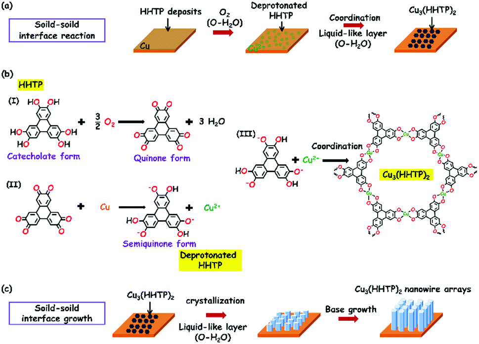
Cu3(HHTP)2 was originally synthesized as bulk solid via a solvothermal method, which exhibited conductivity as high as 20 S m−1.31 Cu3(HHTP)2 has recently been reported to be built only from the stacking of 2D hexagonal extended layers of metal copper (Cu)(II) centers coordinated to deprotonated HHTP linkers following a slipped-parallel (AB) packing mode (Fig. 1b),15 unlike the two distinct types of alternatively stacked layers of Co3(HHTP)2 and Ni3(HHTP)2. The dual-temperature zone CVD method consists of two steps: an organic ligand sublimation, a deposition step and a solid–solid reaction step (Fig. 1a), which enables the in situ growth of conductive Cu3(HHTP)2 NWAs on Cu foils with good orientation.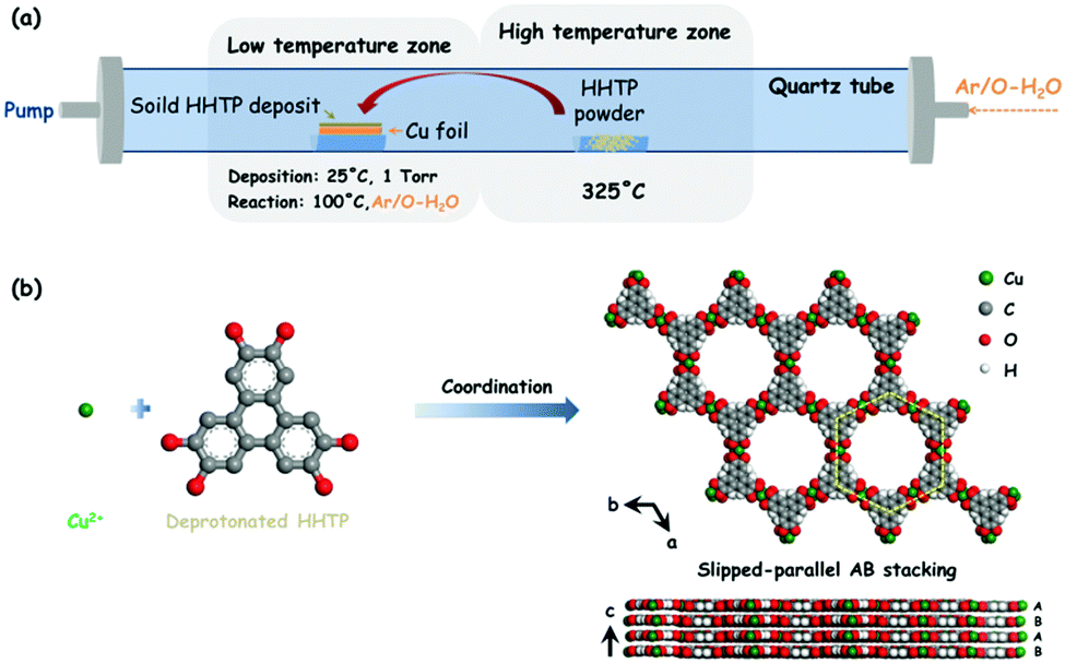 | ||
| Fig. 1 (a) Schematic diagram of dual-temperature zone CVD synthesis of Cu3(HHTP)2 NWAs on Cu foils. The procedure includes an organic ligand sublimation step (high temperature zone) and a solid–solid reaction step (low temperature zone). (b) Illustration of the crystal structure of Cu3(HHTP)2 from slipped-parallel AB stacking of hexagonal layers. | ||
As shown in Fig. 1a, after extensive exploration of the dual-temperature zone CVD conditions, in the present study, HHTP and the polished Cu foil are placed in two separate temperature control zones of the furnace. Before heating, the quartz tube is pumped down to a base pressure of 1 Torr28 to ensure the sublimation of HHTP. The high temperature zone is then heated to 325 °C and kept for 30 min. After sublimation, soild HHTP is deposited on the surface of the polished Cu foil at room temperature. The low temperature zone is then heated to 100 °C and kept for 1 h with an argon/oxygenated water (Ar/O-H2O) mixture flow of 10 sccm to form crystalline Cu3(HHTP)2 NWAs on the Cu foil. It can be obviously observed from the digital photographs (insets of Fig. 2a and b) that the bright yellow Cu foil uniformly turns blue black after the reaction. From a microscopic viewpoint, the scanning electron microscopy (SEM) images (Fig. 2a and b) also reveal that, after synthesis, a large number of oriented nanowires grow uniformly and densely on the smooth surface of the polished Cu foil. The diameter of nanowires was about 200 nm, and its length was about 2 μm. From Fig. 2c, it can be concluded that most of the nanowires possess a structure with a hexagonal column and hexagonal top facet. Moreover, the enlarged images of the red and green dotted boxes in Fig. 2c (Fig. 2d and e) further reveal that the nanowire has a hexagonal layer structure which consists of a number of 2D Cu3(HHTP)2 nanosheets, which conforms to the crystal structure shown in Fig. 2f. For comparison, Cu3(HHTP)2 crystallite powders with an irregular morphology (Fig. S1, ESI†) were synthesized by the normal solvothermal method.
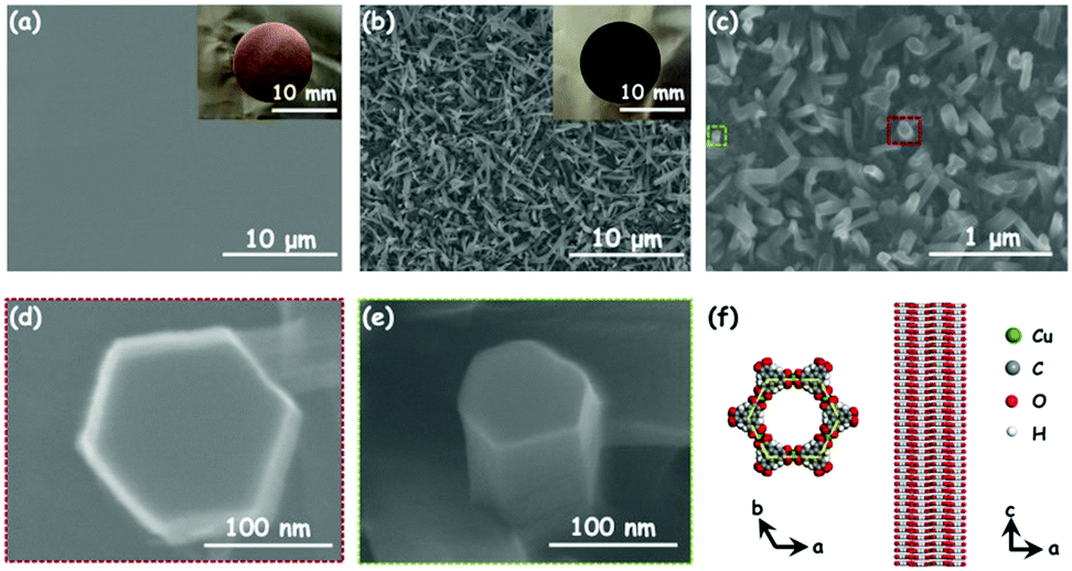 | ||
| Fig. 2 SEM images and digital photographs (inset) of (a) the blank polished Cu foil and (b) Cu3(HHTP)2 NWAs grown on the Cu foil. (c) High-magnification SEM image of Cu3(HHTP)2 NWAs grown on the Cu foil. Enlarged images of (d) the red dotted box and (e) the green dotted box in (c). (f) Layered structure of Cu3(HHTP)2 nanowire from slipped-parallel AB stacking of hexagonal layers. | ||
Taking the crystal structure in Fig. 1b as a model,15 the simulated powder X-ray diffraction (PXRD) spectrum pattern of Cu3(HHTP)2 is calculated by the Reflex module in Materials Studio (Fig. S2, ESI†). As seen in Fig. 3a, the PXRD spectrum pattern of the prepared Cu3(HHTP)2 NWAs on the Cu foil matches the simulated pattern, confirming the crystallinity of the film and demonstrating the successful preparation of Cu3(HHTP)2. The low magnification transmission electron microscopy (TEM) image of a single Cu3(HHTP)2 nanowire is shown in Fig. 3b. The corresponding selected area electron diffraction (SAED) pattern of the nanowire (inset of Fig. 3b) reveals its single crystal feature because of the bright and independent diffraction points. The well-defined diffraction dots in the SAED pattern correspond to the {100} and {300} facets of Cu3(HHTP)2. Additionally, elemental mapping on Cu3(HHTP)2 nanowires obtained from TEM-EDS (EDS, energy-dispersive spectroscopy) also shows a homogeneous distribution of C, O and Cu elements on the Cu3(HHTP)2 nanowire (Fig. 3c). Unfortunately, these nanowires are very sensitive to beam irradiation, resulting in extensive radiolysis damage. As shown in Fig. S3 (ESI†), after exposure to the electron beam for a long time, the nanowire is severely damaged, along with the aggregation of Cu elements. The lattice fringes in the high-resolution TEM (HRTEM) rapidly disappear within a few seconds in spite of its brief visibility, preventing the acquisition of the HRTEM image.
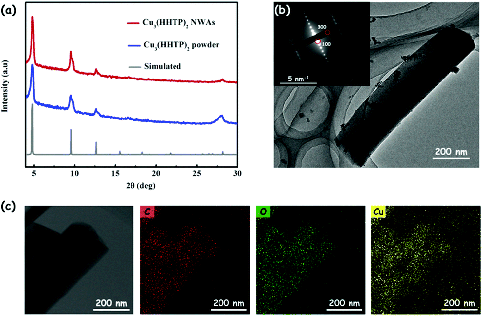 | ||
| Fig. 3 (a) Experimental and simulated PXRD patterns of Cu3(HHTP)2. (b) TEM image and the corresponding SAED pattern (insets, scale bar: 5 nm−1) of Cu3(HHTP)2 nanowires. (c) TEM image of Cu3(HHTP)2 nanowires, and elemental mapping images of carbon, oxygen and copper using TEM-EDS. | ||
Growth mechanism analysis
Our experiments suggest that oxygenated water (O-H2O) is vital to yield crystalline Cu3(HHTP)2. Fig. 4b shows that only HHTP deposits appear on the polished Cu foil under an Ar atmosphere, as confirmed by the PXRD pattern (Khaki line) in Fig. S4a (ESI†). The HHTP deposit can be easily dissolved in ethanol; as a result, in the absence of reaction products, nothing will be left on the polished Cu foil after washing with ethanol. As shown in Fig. 4c and d, after repeatedly washing with ethanol, the surfaces of polished Cu foils are clean without any products in cases of the reactions using Ar or Ar/degassed water (Ar/D-H2O) mixture gases. The PXRD pattern in Fig. S4a (ESI†) (red and purple lines) further illustrates that no phases are detected in the 3° < 2θ < 30° range under an Ar or Ar/D-H2O atmosphere. Note that, under an Ar/O2 mixture atmosphere, lots of nanowires grow on the polished Cu foil (Fig. 4e), and the product survives with ethanol washing. While the EDS analysis of the product obtained by SEM-EDS shows the presence of C, O and Cu elements (Fig. S4b, ESI†), the PXRD pattern (Fig. S4a, green line, ESI†) shows that the product has a weak broad peak around 28° indicating the poor crystallinity of the products. Remarkably, under an Ar/O-H2O mixture atmosphere, a large number of oriented nanowires will uniformly and densely grow on the polished Cu foil (Fig. 4f), exhibiting high crystallinity (Fig. S4a, blue line, ESI†). All these results indicate that O2 is the key to generate Cu3(HHTP)2 nanowires, and H2O is vital to enable crystallization of Cu3(HHTP)2 nanowires.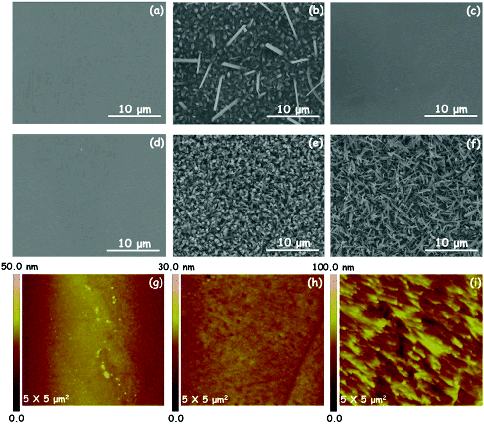 | ||
| Fig. 4 SEM images of the (a) blank polished Cu foil, (b) HHTP deposit on the polished Cu foil, and products obtained under an (c) Ar, (d) Ar/D-H2O, (e) Ar/O2 and (f) Ar/O-H2O atmosphere. AFM topographic images of (g) the blank polished Cu foil, products obtained under an (h) Ar and (i) Ar/O-H2O atmosphere after the treatment of diluted hydrochloric acid. | ||
A solid–solid interface reaction assisted by O2 and H2O is intriguing beyond the reaction in a conventional liquid or gas medium system. Understanding the underlying mechanism is very important for generalizing this method to other materials systems, and it is essential to know how solid Cu and the organic source convert to active metal ions or individual organic molecules that participate in the nucleation and growth process of the desired MOFs. Firstly, HHTP is a redox-active linker that can undergo reversible interconversions between the catecholate, semiquinone and quinone forms in the presence of O2 (Fig. 5a and b).31,32 The quinone form with a strong oxidation tendency is capable of converting Cu into Cu2+, and then transforms into the semiquinone form (i.e., deprotonated HHTP) that coordinates with the Cu2+. Control experiments were performed to provide evidence for the conversion of Cu to Cu2+. Briefly, the Cu foil was placed in an aqueous solution of HHTP at 100 °C for 30 min. It was found that large amounts of Cu2+ were subsequently detected in the solution, demonstrating that the Cu atom loses electrons to become Cu2+ during the reaction. In addition, atomic force microscopy (AFM) imaging was employed to directly investigate the surface morphology change of products after reactions. Note that the samples were treated with diluted hydrochloric acid for removing HHTP or MOFs. For comparison, the blank polished Cu foil has a very smooth surface (Fig. 4g). In the case of using Ar gas in the reaction system, the surface of the Cu foil is similar to that of blank Cu, confirming that the deposited HHTP does not react with the Cu surface. In sharp contrast, the surface of the Cu foil appears very rough when as-grown Cu3(HHTP)2 NWAs are removed by diluted hydrochloric acid, demonstrating the assumption of Cu for the MOF formation. The presence of the constitutive elements of Cu3(HHTP)2 NWAs (C, O, and Cu; Fig. S5a, ESI†) is confirmed by the X-ray photoelectron (XPS) survey spectrum. The Cu 2p region of the Cu3(HHTP)2 NWA spectra (Fig. S5b, ESI†) shows the main Cu(2p3/2) and Cu(2p1/2) components at 935.1 eV and 954.5 eV, respectively, in which the Cu 2p3/2 peak exhibits a dominant peak at ∼935 eV for the Cu2+ state and a weak peak at ∼933 eV for the Cu+ state, respectively. The electron paramagnetic resonance (EPR) spectrum of the Cu3(HHTP)2 NWAs shows a near-symmetric signal at g = 2.105 (Fig. S5c, ESI†), which is a characteristic feature of an unpaired electron localized on a ligand orbital and matches well with the values of semiquinonate based complexes.31
 | ||
| Fig. 5 Formation mechanism of the Cu3(HHTP)2 NWAs on the Cu foil showing (a) the solid–solid interface reaction, (b and c) three step reactions consisting of the conversion of Cu to Cu2+ and MOF formation, and a solid–solid base-growth process. | ||
The above observations can be rationalized into a MOF formation process consisting of two successive steps as follows (Fig. 5). Firstly, O2 in O-H2O oxidizes the HHTP into the quinone form33 that changes to the semiquinone form (deprotonated HHTP) by converting Cu to Cu2+. Secondly, Cu2+ coordinates with the deprotonated HHTP to form Cu3(HHTP)2 nuclei, in which the diffusion process of these species for proper crystallization is likely assisted with a trace amount of liquid H2O.21 MOF growth is ensured by a continuous supply of Cu2+ and deprotonated HHTP.
More careful analysis and experiments show that this growth is described by a base-growth mode that has not been identified previously in liquid medium MOF growth or solid–gas CVD systems. For example, Fig. S6 (ESI†) shows several growth stages of Cu3(HHTP)2 nanowires on Cu foils. Apparently, while the nucleation density of Cu3(HHTP)2 nanowires on the Cu surface remains essentially the same as a function of growth time, the growth along the c-axis is continuous as time goes on, reflecting a base-growth mode. Moreover, by controlling the amount of deposited HHTP on Cu, the nucleation density of MOF nanowires is reduced to eliminate the lateral interaction among nanowires during the growth. In this case, Cu3(HHTP)2 nanowires exhibit a smaller top and a bigger base due to the greater abundance Cu2+ at the base (Fig. S7, ESI†), which is a typical observation in base-growth mode (Fig. 5c). In addition, the generated nanowires in the absence of H2O further demonstrate the base-growth mode. Finally, our method allows the space to control the supply of Cu, and such a control is demonstrated by MOF growth on graphene/Cu foil. The graphene layer acts as a barrier layer for Cu conversion and diffusion, leading to a restricted growth in the c-axis direction (Fig. S8, ESI†). Note that MOF crystals are preferentially grown along Cu steps, consistent with the point that these sites are more energetic for MOF nucleation. This result provides a way for controlling the dimensionality of MOF crystals.
Specific surface area and electrical conductivity
Fig. S9a and b (ESI†) reveal the nitrogen adsorption–desorption isotherms and pore size distribution of Cu3(HHTP)2 NWAs, respectively. The remarkable gas uptake and release in Fig. S9a (ESI†) indicate the permanent porosity of Cu3(HHTP)2 NWAs.4 The specific surface area calculated by the Brunauer–Emmett–Teller (BET) method is 475 m2 g−1. From Fig. S9b (ESI†), it can be seen that the main pore type of Cu3(HHTP)2 NWAs is micropore, and the pore size is in the range of 2–15 nm. To characterize the electrical properties of Cu3(HHTP)2, the two-probe I–V curve of a single Cu3(HHTP)2 nanowire was measured at 300 K with Au electrodes as the contact material, which shows a linear response that denotes ohmic contacts between the Au electrodes and Cu3(HHTP)2 (Fig. S9c, ESI†). The conductance of the Cu3(HHTP)2 nanowire is calculated to be about 20.9 ± 2 S m−1, indicating that the Cu3(HHTP)2 NWAs on the Cu foil prepared by the dual-temperature zone CVD method are sufficient for the realization of conductive additive-free electrode design.6 The in situ growth processes can offer good adhesion between conductive MOF nanowires and the Cu current collector to avoid using conductive additives and binders, and to ensure effective surface area of the electrode. Besides, the one-dimensional (1D) nanostructures can provide direct, efficient pathways for electron transport, and the direct contact between each nanowire and the Cu current collector can accelerate electron transport.34 Moreover, the 1D hexagonal channels along the growth direction of the Cu3(HHTP)2 NWAs will accelerate the transport of electrolyte ions to achieve high rate performance for supercapacitors.19Supercapacitor performance
To evaluate the electrochemical performances of the Cu3(HHTP)2 NWAs on the Cu foil, the whole ensemble was used as the sole working electrode in a three-electrode cell with Ag/AgCl as the reference electrode and a platinum plate as a counter electrode, which was executed in 1 M KCl aqueous electrolyte. As shown in Fig. 6a, cyclic voltammetry (CV) curves are in quasi-rectangular shape without distinct redox peaks when cycled cathodically between the open circuit potentials of −0.02 V and −0.6 V (vs. Ag/AgCl), indicating that the electrochemical performance is mainly dominated by the electric double-layer capacitive behavior in the sweep range.35,36 As shown in Fig. S10 (ESI†), the CV curve of the current collector blank copper foil exhibits an almost flat shape, and therefore the specific capacitance contributed by the copper foil in the Cu3(HHTP)2 NWA electrode can be neglected. However, compared with a rectangle, the curves show some deformation, which is mainly caused by the pseudocapacitance introduced by metal ions in the structure of Cu3(HHTP)2 NWAs. Along with the increase of scan rate, the curve of the Cu3(HHTP)2 NWA electrode remains unchanged without significant distortion, implying its remarkable rate performance and capacitive reversibility.35Fig. 6b demonstrates the galvanostatic charge/discharge (GCD) curves of the Cu3(HHTP)2 NWA electrode tested in the potential range of −0.6 to −0.02 V at different current densities. The nearly linear charge/discharge curves further confirm the dominant electric double-layer capacitive charge storage mechanism.35,36 Nevertheless, the charge/discharge curves at current densities of 0.5 and 1.0 A g−1 are asymmetric, which is probably caused by some irreversible faradaic processes.36,37 Besides, the charge/discharge curve displays a much lower voltage drop at the beginning of the discharge process, which indicates that the Cu3(HHTP)2 NWA electrode has a certain internal resistance.36 The specific gravimetric capacitances are calculated from the galvanostatic discharge curves at various current densities, which are 215.9, 206.7, 195.2, 168.1, and 155.2 F g−1 at 0.5, 1, 2, 5, and 10 A g−1, respectively. The Cu3(HHTP)2 NWA electrode retains 71.9% of its capacitance upon increasing the current density from 0.5 to 10 A g−1. As shown in Fig. 6c, the Cu3(HHTP)2 NWA electrode exhibits favorable stability after 5000 GCD cycles between −0.6 V and −0.02 V at 10 A g−1. After 5000 cycles, the electrode retains 79.7% of its initial capacitance. The gravimetric capacitances and cycling performance are comparable to those of other MOF-based supercapacitors with conductive additives.19,38–40 The electrochemical stability of the Cu3(HHTP)2 NWAs under the cycling conditions was detected by PXRD measurements. There is a negligible change at the position of 2θ ∼ 28° of the PXRD pattern relative to the pristine NWAs (Fig. S11, ESI†), suggesting that the Cu3(HHTP)2 NWAs can remain intact upon extensive cycling. The excellent electrochemical stability of the Cu3(HHTP)2 NWAs ensures their use in low-cost and nonflammable KCl aqueous electrolyte.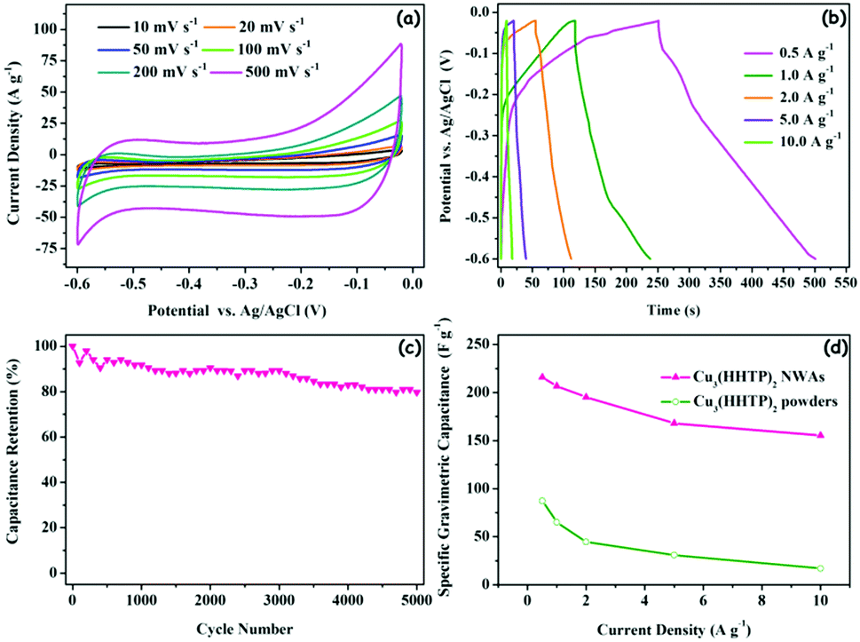 | ||
| Fig. 6 Electrochemical performances of Cu3(HHTP)2 NWAs using a three-electrode cell in 1 mol L−1 KCl. (a) CV curves collected at different scan rates. (b) GCD curves at different current densities. (c) Capacitance retention collected by galvanostatic charge discharge at 10 A g−1 for 5000 cycles. (d) Rate-dependent specific capacitance. | ||
For comparison, Cu3(HHTP)2 crystallite powders synthesized by the normal solvothermal method were mixed with a polymer binder without conductive additives, and then coated onto a Cu foil to prepare a powder electrode by the traditional coating method. Remarkably, the electrode based on Cu3(HHTP)2 NWAs exhibits two times higher specific gravimetric capacitance than that based on Cu3(HHTP)2 powders (Fig. 6d). Besides, the Cu3(HHTP)2 NWA electrode retains 71.9% of its capacitance with increasing current density from 0.5 to 10 A g−1; in sharp contrast, the Cu3(HHTP)2 powder electrode retains 19.7% of its capacitance with the same change in current density. As displayed in Fig. S10b (ESI†), electrochemical impedance spectra (EIS) were measured at the open-circuit potential for explaining the above results. The intersection at the real impedance axis reflects the equivalent ohmic resistance, which is the totality of the ionic resistance, contact resistance and intrinsic resistance of active materials.41 The radius of semicircle in the high frequency region represents the charge transfer resistance at the electrode/electrolyte interface.42 The slope derived from the linear part in the low-frequency region reflects the diffusive resistance of the electrolyte, and a higher value indicates a lower diffusive resistance.38 It can be obviously seen that the ohmic resistance, charge transfer resistance at the electrode/electrolyte interface and diffusive resistance of the electrolyte in the Cu3(HHTP)2 NWA electrode are all significantly lower than those of the Cu3(HHTP)2 powder electrode. The decrease of resistance can be attributed to the in situ growth of single crystal nanowire arrays on the Cu foil. Unlike the powder electrode, the in situ growth processes offer good adhesion between MOF nanowires and the Cu current collector, lowering the contact resistance between them. 1D nanostructures provide direct and efficient pathways for fast electron transport at the electrode/electrolyte interface.34 Besides, the 1D hexagonal channels along the growth direction of the Cu3(HHTP)2 NWAs will accelerate the transport of electrolyte ions to achieve faster diffusive speed.19 The unique geometry of MOF NWAs and excellent contact between NWAs and Cu explain why the electrode based on Cu3(HHTP)2 NWAs prepared by the CVD method has much higher rate performance than the electrode based on Cu3(HHTP)2 powders synthesized by the normal solvothermal method.
To further evaluate the practicality of the Cu3(HHTP)2 NWA electrode, two-electrode symmetrical supercapacitor cells were fabricated by employing two identical round slices of Cu3(HHTP)2 NWA electrodes (Φ = 1.2 cm) as the positive and negative electrodes with a piece of separator membrane in 1 M KCl. Fig. 7a and b present the CV and GCD curves of the Cu3(HHTP)2 NWAs-based supercapacitor, confirming its double-layer behavior. With increasing scan rates, no apparent distortions of CV curves are observed, indicating the excellent capacitive behavior of the supercapacitor. The specific gravimetric capacitances are calculated to be 239.1, 195.3, 143.6, 137.5 and 130.8 F g−1 at current densities of 0.25, 0.5, 1.0, 2.5, and 5.0 A g−1 (based on the mass of total active materials), respectively, corresponding to 50.3, 41.1, 30.2, 28.9 and 27.4 μF cm−2 for specific surface area normalized capacitance of the device, respectively. The value of 41.1 μF cm−2 for 0.5 A g−1 exceeds the reported values for supercapacitors based on microporous carbon, carbon nanocages, carbon capsules, carbon nanotubes, carbon nanohorns and thermally exfoliated graphene (7.6–22.7 μF cm−2), and is comparable to the value of a supercapacitor based on composite graphene/carbon nanotube materials (68.9 μF cm−2) (Fig. 7c; and Table S1, ESI†).43–49 In addition, the Cu3(HHTP)2 NWA supercapacitor exhibits a capacitance retention as high as 54.7% with increasing current density from 0.25 to 5 A g−1 (Fig. S12a, ESI†). The Cu3(HHTP)2 NWA supercapacitor has good cycling stability after 5000 GCD cycles between 0 V and 0.8 V at 5 A g−1, which retains 79.9% of its initial capacitance (Fig. 7d). The changes in gravimetric energy density and gravimetric power density along with the corresponding current density are shown in Fig. S12b (ESI†). Notably, at a current density of 0.5 A g−1, the Cu3(HHTP)2 NWA supercapacitor shows a gravimetric energy density of 4.3 W h kg−1 with a gravimetric power density of 200 W kg−1. This value compares favorably to the behavior of a previously reported Cu3(HHTP)2 NWA-based device (2.6 W h kg−1 at 200 W kg−1),19 and is comparable to the value of supercapacitors based on carbon materials which used aqueous electrolytes.50
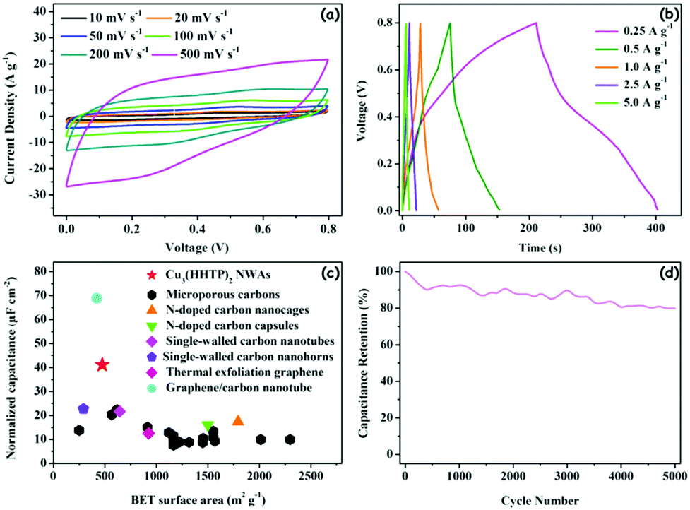 | ||
| Fig. 7 Device performances of the Cu3(HHTP)2 NWA-based supercapacitor: (a) CV curves at different scan rates. (b) GCD curves at different current densities. (c) Performance comparison of symmetric supercapacitors based on Cu3(HHTP)2 NWAs and carbon materials. (d) Cycling performance. | ||
Finally, as a demonstration of generality of our solid–solid interface growth of conductive MOFs, Fe3(HHB)2 was successfully prepared under similar experimental conditions to Cu3(HHTP)2 NWAs (Fig. S13, ESI†).
Conclusions
In summary, oriented MOF NWAs of conductive Cu3(HHTP)2in situ grown on the interface between a solid Cu foil and a solid organic precursor have been successfully prepared by a dual-temperature zone CVD-assisted method for the first time. The role of oxygenated water in the formation of crystalline Cu3(HHTP)2 NWAs is elucidated. O2 is the key to generate Cu3(HHTP)2 nanowires, and H2O is vital to enable crystallization of Cu3(HHTP)2 nanowires. A base-growth mode is proposed in solid–solid interface growth, which is supported by experiments. We believe that the concept of solid–solid interface growth opens up a door for the production of a wide variety of potential conductive MOFs using the dual-temperature zone CVD method. In addition, the thus produced Cu3(HHTP)2 NWAs on the Cu foil can be directly used in a symmetrical supercapacitor without conductive additives and binders, and the supercapacitor achieves a high specific surface area normalized capacitance of 41.1 μF cm−2 for 0.5 A g−1, which is beyond the previously reported values of supercapacitors based on porous carbon (such as microporous carbon, carbon nanotubes and thermally exfoliated graphene). In general, the solid–solid reaction approach and direct supercapacitor application are appealing in the production of MOFs and their application.Conflicts of interest
There are no conflicts to declare. The manuscript was written through contributions of all authors. All authors have given approval to the final version of the manuscript.Acknowledgements
This work was supported by the National Basic Research Program of China (2016YFA0200101), the National Natural Science Foundation of China (21633012 and 61890940), the Chinese Academy of Sciences and the Strategic Priority Research Program of the Chinese Academy of Sciences (XDB30000000 and XDB12030100), the China Postdoctoral Science Foundation (2018M630207), and the CAS Key Research Program of Frontier Sciences (QYZDY-SSW-SLH029).References
- M. K. Smith, K. E. Jensen, P. A. Pivak and K. A. Mirica, Chem. Mater., 2016, 28, 5264–5268 CrossRef CAS.
- M. S. Yao, X. J. Lv, Z. H. Fu, W. H. Li, W. H. Deng, G. D. Wu and G. Xu, Angew. Chem., Int. Ed., 2017, 56, 16510–16514 CrossRef CAS.
- D. Sheberla, J. C. Bachman, J. S. Elias, C. J. Sun, Y. Shao-Horn and M. Dinca, Nat. Mater., 2017, 16, 220–224 CrossRef CAS.
- G. Wu, J. Huang, Y. Zang, J. He and G. Xu, J. Am. Chem. Soc., 2017, 139, 1360–1363 CrossRef CAS PubMed.
- N. Lahiri, N. Lotfizadeh, R. Tsuchikawa, V. V. Deshpande and J. Louie, J. Am. Chem. Soc., 2017, 139, 19–22 CrossRef CAS.
- D. Feng, T. Lei, M. R. Lukatskaya, J. Park, Z. Huang, M. Lee, L. Shaw, S. Chen, A. A. Yakovenko, A. Kulkarni, J. Xiao, K. Fredrickson, J. B. Tok, X. Zou, Y. Cui and Z. Bao, Nat. Energy, 2018, 3, 30–36 CrossRef CAS.
- V. Rubio-Gimenez, N. Almora-Barrios, G. Escorcia-Ariza, M. Galbiati, M. Sessolo, S. Tatay and C. Marti-Gastaldo, Angew. Chem., Int. Ed., 2018, 57, 15086–15090 CrossRef CAS.
- H. Wang, Q. L. Zhu, R. Zou and Q. Xu, Chem, 2017, 2, 52–80 CAS.
- Z. Liang, C. Qu, W. Guo, R. Zou and Q. Xu, Adv. Mater., 2017, 30, 1702891 CrossRef.
- L. Wang, X. Feng, L. Ren, Q. Piao, J. Zhong, Y. Wang, H. Li, Y. Chen and B. Wang, J. Am. Chem. Soc., 2015, 137, 4920–4923 CrossRef CAS.
- K. M. Choi, H. M. Jeong, J. H. Park, Y. B. Zhang, J. K. Kang and O. M. Yaghi, ACS Nano, 2014, 8, 7451–7457 CrossRef CAS.
- L. Ma, J. M. Falkowski, C. Abney and W. Lin, Nat. Chem., 2010, 2, 838 CrossRef CAS.
- O. K. Farha, A. Özgür Yazaydın, I. Eryazici, C. D. Malliakas, B. G. Hauser, M. G. Kanatzidis, S. T. Nguyen, R. Q. Snurr and J. T. Hupp, Nat. Chem., 2010, 2, 944 CrossRef CAS.
- P. Horcajada, T. Chalati, C. Serre, B. Gillet, C. Sebrie, T. Baati, J. F. Eubank, D. Heurtaux, P. Clayette, C. Kreuz, J. S. Chang, Y. K. Hwang, V. Marsaud, P. N. Bories, L. Cynober, S. Gil, G. Férey, P. Couvreur and R. Gref, Nat. Mater., 2009, 9, 172 CrossRef.
- V. Rubio-Gimenez, M. Galbiati, J. Castells-Gil, N. Almora-Barrios, J. Navarro-Sanchez, G. Escorcia-Ariza, M. Mattera, T. Arnold, J. Rawle, S. Tatay, E. Coronado and C. Marti-Gastaldo, Adv. Mater., 2018, 30, 1704291 CrossRef.
- L. Sun, M. G. Campbell and M. Dincă, Angew. Chem., Int. Ed., 2016, 55, 3566–3579 CrossRef CAS.
- D. Sheberla, L. Sun, M. A. Blood-Forsythe, S. Er, C. R. Wade, C. K. Brozek, A. Aspuru-Guzik and M. Dinca, J. Am. Chem. Soc., 2014, 136, 8859–8862 CrossRef CAS.
- T. Deng, W. Zhang, O. Arcelus, D. Wang, X. Shi, X. Zhang, J. Carrasco, T. Rojo and W. Zheng, Commun. Chem., 2018, 1, 6 CrossRef.
- W. H. Li, K. Ding, H. R. Tian, M. S. Yao, B. Nath, W. H. Deng, Y. Wang and G. Xu, Adv. Funct. Mater., 2017, 27, 1702067 CrossRef.
- P. Falcaro, R. Ricco, C. M. Doherty, K. Liang, A. J. Hill and M. J. Styles, Chem. Soc. Rev., 2014, 43, 5513–5560 RSC.
- I. Stassen, M. Styles, G. Grenci, H. V. Gorp, W. Vanderlinden, S. D. Feyter, P. Falcaro, D. D. Vos, P. Vereecken and R. Ameloot, Nat. Mater., 2016, 15, 304–310 CrossRef CAS.
- X. Huang, P. Sheng, Z. Tu, F. Zhang, J. Wang, H. Geng, Y. Zou, C. A. Di, Y. Yi, Y. Sun, W. Xu and D. Zhu, Nat. Commun., 2015, 6, 7408 CrossRef CAS.
- P. M. Martin, Handbook of deposition technologies for films and coatings: Science, applications and technology, William Andrew, 2009 Search PubMed.
- I. Stassen, D. De Vos and R. Ameloot, Chem. – Eur. J., 2016, 22, 14452–14460 CrossRef CAS.
- X. Ma, P. Kumar, N. Mittal, A. Khlyustova, P. Daoutidis, K. A. Mkhoyan and M. Tsapatsis, Science, 2018, 361, 1008–1011 CrossRef CAS.
- M. Ko, L. Mendecki and K. A. Mirica, Chem. Commun., 2018, 54, 7873–7891 RSC.
- J. Park, A. C. Hinckley, Z. Huang, D. Feng, A. Yakovenko, M. Lee, S. Chen, X. Zou and Z. Bao, J. Am. Chem. Soc., 2018, 140, 14533–14537 CrossRef CAS.
- N. A. A. Zwaneveld, R. Pawlak, M. Abel, D. Catalin, D. Gigmes, D. Bertin and L. Porte, J. Am. Chem. Soc., 2008, 130, 6678–6679 CrossRef CAS.
- J. Mahmood, E. K. Lee, M. Jung, D. Shin, H. J. Choi, J. M. Seo, S. M. Jung, D. Kim, F. Li, M. S. Lah, N. Park, H. J. Shin, J. H. Oh and J. B. Baek, Proc. Natl. Acad. Sci. U. S. A., 2016, 113, 7414–7419 CrossRef CAS.
- J. H. Dou, L. Sun, Y. Ge, W. Li, C. H. Hendon, J. Li, S. Gul, J. Yano, E. A. Stach and M. Dinca, J. Am. Chem. Soc., 2017, 139, 13608–13611 CrossRef CAS.
- M. Hmadeh, Z. Lu, Z. Liu, F. Gándara, H. Furukawa, S. Wan, V. Augustyn, R. Chang, L. Liao, F. Zhou, E. Perre, V. Ozolins, K. Suenaga, X. Duan, B. Dunn, Y. Yamamto, O. Terasaki and O. M. Yaghi, Chem. Mater., 2012, 24, 3511–3513 CrossRef CAS.
- A. M. Barthram, R. L. Cleary, R. Kowallick and M. D. Ward, Chem. Commun., 1998, 2695–2696 RSC.
- J. B. Simonsen, Surf. Sci., 2010, 604, 1300–1309 CrossRef CAS.
- L. Zheng, Y. Xu, D. Jin and Y. Xie, J. Mater. Chem., 2010, 20, 7135–7143 RSC.
- H. Y. Wang, B. Li, J. X. Teng, H. L. Zhu, Y. X. Qi, L. W. Yin, H. Li, N. Lun and Y. J. Bai, Electrochim. Acta, 2017, 257, 56–63 CrossRef CAS.
- L. Liu, Y. Yan, Z. Cai, S. Lin and X. Hu, Adv. Mater. Interfaces, 2018, 5, 1701548 CrossRef.
- M. Beidaghi and C. Wang, Adv. Funct. Mater., 2012, 22, 4500 CrossRef CAS.
- G. Zhu, H. Wen, M. Ma, W. Wang, L. Yang, L. Wang, X. Shi, X. Cheng, X. Sun and Y. Yao, Chem. Commun., 2018, 54, 10499–10502 RSC.
- R. Ramachandran, C. Zhao, D. Luo, K. Wang and F. Wang, Electrochim. Acta, 2018, 267, 170–180 CrossRef CAS.
- R. Ramachandran, C. Zhao, D. Luo, K. Wang and F. Wang, Appl. Surf. Sci., 2018, 460, 33–39 CrossRef CAS.
- M. Kong, Z. Wang, W. Wang, M. Ma, D. Liu, S. Hao, R. Kong, G. Du, A. M. Asiri, Y. Yao and X. Sun, Chem. – Eur. J., 2017, 23, 4435–4441 CrossRef CAS.
- X. Zhang, J. Luo, P. Tang, X. Ye, X. Peng, H. Tang, S. G. Sun and J. Fransaer, Nano Energy, 2017, 31, 311–321 CrossRef CAS.
- T. A. Centeno and F. Stoeckli, Electrochim. Acta, 2011, 56, 7334–7339 CrossRef CAS.
- J. Zhao, H. Lai, Z. Lyu, Y. Jiang, K. Xie, X. Wang, Q. Wu, L. Yang, Z. Jin, Y. Ma, J. Liu and Z. Hu, Adv. Mater., 2015, 27, 3541–3545 CrossRef CAS PubMed.
- G. A. Ferrero, A. B. Fuertes and M. Sevilla, J. Mater. Chem. A, 2015, 3, 2914–2923 RSC.
- F. Picó, J. M. Rojo, M. L. Sanjuán, A. Ansón, A. M. Benito, M. A. Callejas, W. K. Maser and M. T. Martínez, J. Electrochem. Soc., 2004, 151, A831–A837 CrossRef.
- C. M. Yang, Y. J. Kim, M. Endo, H. Kanoh, M. Yudasaka, S. Iijima and K. Kaneko, J. Am. Chem. Soc., 2007, 129, 20–21 CrossRef CAS.
- S. R. C. Vivekchand, C. S. Rout, K. S. Subrahmanyam, A. Govindaraj and C. N. R. Rao, J. Chem. Sci., 2008, 120, 9–13 CrossRef CAS.
- Q. Cheng, J. Tang, J. Ma, H. Zhang, N. Shinya and L. C. Qin, Phys. Chem. Chem. Phys., 2011, 13, 17615–17624 RSC.
- X. Chen, R. Paul and L. Dai, Natl. Sci. Rev., 2017, 4, 453–489 CrossRef CAS.
Footnote |
| † Electronic supplementary information (ESI) available. See DOI: 10.1039/c9qm00527g |
| This journal is © the Partner Organisations 2020 |