
 Open Access Article
 This Open Access Article is licensed under a Creative Commons Attribution-Non Commercial 3.0 Unported Licence
Spin-wave spectroscopy of individual ferromagnetic nanodisks†
Oleksandr V.
Dobrovolskiy
 *a,
Sergey A.
Bunyaev
b,
Nikolay R.
Vovk
bc,
David
Navas
bd,
Pawel
Gruszecki
ef,
Maciej
Krawczyk
e,
Roland
Sachser
g,
Michael
Huth
g,
Andrii V.
Chumak
a,
Konstantin Y.
Guslienko
hi and
Gleb N.
Kakazei
b
*a,
Sergey A.
Bunyaev
b,
Nikolay R.
Vovk
bc,
David
Navas
bd,
Pawel
Gruszecki
ef,
Maciej
Krawczyk
e,
Roland
Sachser
g,
Michael
Huth
g,
Andrii V.
Chumak
a,
Konstantin Y.
Guslienko
hi and
Gleb N.
Kakazei
b
aFaculty of Physics, University of Vienna, Boltzmanngasse 5, 1090 Vienna, Austria. E-mail: oleksandr.dobrovolskiy@univie.ac.at; Tel: +43 14277 73920
bInstitute of Physics for Advanced Materials, Nanotechnology and Photonics (IFIMUP)/Departamento de Física e Astronomia, Universidade do Porto, Rua Campo Alegre 687, 4169-007 Porto, Portugal
cDepartment of Physics, V. N. Karazin Kharkiv National University, Svobody Sq. 4, Kharkiv 61022, Ukraine
dInstituto de Ciencia de Materiales de Madrid, ICMM-CSIC, 28049 Madrid, Spain
eFaculty of Physics, Adam Mickiewicz University in Poznań, Uniwersytetu Poznańskiego St. 2, 61-614 Poznań, Poland
fInstitute of Molecular Physics, Polish Academy of Sciences, Mariana Smoluchowskiego St. 17, 60-179 Poznań, Poland
gInstitute of Physics, Goethe University, Max-von-Laue-Str. 1, 60438 Frankfurt am Main, Germany
hDivision de Fisica de Materiales, Depto. Polimeros y Materiales Avanzados: Fisica, Quimica y Tecnologia, Universidad del Pais Vasco, UPV/EHU, Paseo M. Lardizabal 3, 20018 San Sebastian, Spain
iIKERBASQUE, the Basque Foundation for Science, Plaza Euskadi 5, 48009 Bilbao, Spain
First published on 6th October 2020
Abstract
The increasing demand for nanoscale magnetic devices requires development of 3D magnetic nanostructures. In this regard, focused electron beam induced deposition (FEBID) is a technique of choice for direct-writing of complex nano-architectures with applications in nanomagnetism, magnon spintronics, and superconducting electronics. However, intrinsic properties of nanomagnets are often poorly known and can hardly be assessed by local optical probe techniques. Here, an original spatially resolved approach is demonstrated for spin-wave spectroscopy of individual circular magnetic elements with sample volumes down to about 10−3 μm3. The key component of the setup is a coplanar waveguide whose microsized central part is placed over a movable substrate with well-separated CoFe-FEBID nanodisks which exhibit standing spin-wave resonances. The circular symmetry of the disks allows for the deduction of the saturation magnetization and the exchange stiffness of the material using an analytical theory. A good correspondence between the results of analytical calculations and micromagnetic simulations is revealed, indicating a validity of the used analytical model going beyond the initial thin-disk approximation used in the theoretical derivation. The presented approach is especially valuable for the characterization of direct-write magnetic elements opening new horizons for 3D nanomagnetism and magnonics.
1 Introduction
Patterned nanomagnets have traditionally been two-dimensional planar structures. Recent work, however, is expanding nanomagnetism into the third dimension.1–3 This expansion is triggered by the development of advanced synthesis methods4,5 and the discovery of novel geometry- and topology-induced effects.6 Among the various nanofabrication techniques, focused electron beam-induced deposition (FEBID) has unique advantages for 3D nanomagnetism,2,3,7 magnonics8,9 and superconducting electronics of the fluxonic type10,11 as the magnetic properties of direct-write structures can be varied by selecting a writing strategy and beam parameters,5 as well as via post-growth irradiation of structures with ions12–14 and electrons.15 In the context of superconductivity, hybrid ferromagnet/superconductor structures are used for the manipulation of magnetic flux quanta16,17 and provide access to investigations of odd-frequency spin-triplet superconductivity.18,19 In the domain of magnonics, FEBID allows for the realization of 3D magnonic crystals20–22 and magnonic conduits with graded refractive index.23 However, the magnetic parameters of individual nanoelements are often poorly known and can hardly be assessed by local optical probe techniques, such as Brillouin light scattering (BLS)24 and magneto-optical Kerr microscopy,25 having a spatial resolution limit of about 300 nm. For resolving the magnetization dynamics at GHz frequencies on the length scale of a few tens of nm more sophisticated techniques are required. For instance, near-field BLS allows for imaging the edge mode dynamics with a resolution of about 50 nm (ref. 26) and X-ray microscopy provides dynamic magnetization imaging with a resolution as fine as 30 nm.27,28 At the same time, so far only few BLS studies are based on near-field optics while for X-ray imaging large-scale facilities are required. Therefore, the development of easy-to-use experimental techniques for the deduction of magnetic properties of individual nanoelements is of crucial importance.Ferromagnetic resonance (FMR) is the method of choice for a quantitative analysis of saturation magnetization, magnetic anisotropy, dipolar interactions, relaxation of magnetization, and the structural quality and (in)homogeneity of magnetic materials.29–32 However, the sensitivity of FMR is often not high enough for the detection of signals from individual magnetic nanoelements. The sensitivity of the cavity-based FMR is estimated as ≃1010 spins and it can reach 108–109 spins for its broadband strip-line counterpart.33 In order to compensate for poor signal-to noise ratio (SNR), usually many magnetic elements are arranged in arrays.34,35 However, in case of ensemble measurements the signal analysis is often complicated by interactions between the individual elements and by the distribution in their sizes and properties. This is why a number of alternative FMR-based approaches have been introduced for studying magnetization dynamics in single nanomagnets, see e.g.ref. 36, 37 and 38. Among these approaches, FMR force microscopy (FMRFM)39–42,66 and microresonator-based FMR (MRFMR)43,44 have a high sensitivity of ≃106 spins and allow for probing ≃100 nm-large samples or areas of thin films.41,44,45 However, separate resonators are needed for each individual sample in MRFMR, and a quantitative analysis of the material parameters by FMRFM is not straightforward when the size of the magnetic tip becomes comparable with the size of the sample.
An ultrahigh sensitivity of FMR measurements reached by using a microwave interferometer has been demonstrated to allow for resolving uniform-mode FMR signals from down to 100 nm-diameter, 5 nm-thick single nanodots.37 However, this technique is quite delicate and it requires the sample to be integrated into the sensing unit as it is grown directly on top of a coplanar waveguide. It should be stressed that the compositional and magnetic properties of FEBID structures fabricated on metallic and insulating substrates can be different since their deposition is dependent on the yield of secondary electrons and the diffusion of precursor molecules.5 Furthermore, this issue is also crucial for magnetic materials for which the choice of the substrate and the quality of its surface is decisive for the quality and magnetic properties of the sample, such as e.g. YIG thin films on gadolinium gallium garnet substrates.42,46
An alternative approach to achieve large filling factors and high coupling efficiencies is to use microwave strip-lines whose active parts are narrow and short in conjunction with samples themselves being used as resonators. A small width of the strip-line allows for larger local microwave fields and, hence, higher microwave power-to-field conversion efficiencies.47 A short length of the narrow, sensitive part of the strip-line allows for spatially-resolved microwave measurements. Due to the confinement of spin waves various resonant modes appear in nanoelements.48 However, an analytical description of the magnetization dynamics in elements of arbitrary shape is barely feasible, and spin-wave eigenfrequencies can be calculated explicitly only in the few cases of simplest (e.g. circular) symmetry.49 In particular, higher-order modes of spin-wave excitations in circular elements with radii of few hundreds nm are dipole-exchange spin waves with wavelengths λ ≃ 50 nm. Such spin waves are appreciably influenced by the exchange interaction and are, in particular, objects of current investigations in nanomagnonics50 aiming at the operation with fast, exchange-dominated spin waves.27,51,52
Here, we demonstrate spatially resolved spin-wave spectroscopy for the assessment of magnetic properties of individual circular magnetic elements with radii down to 100 nm. Employing a coplanar waveguide whose 2 × 4 μm2-large active part is placed over a movable substrate with well-separated circular magnetic nanoelements we detect standing spin-wave resonances from individual 40 nm-thick CoFe-FEBID nanodisks. These are the smallest magnetic elements successfully probed in the presence of a uniform microwave field so far. In addition to the main resonance peak, we distinguish up to 9 higher-order spin-wave excitation modes and deduce the saturation magnetization and the exchange stiffness of individual elements with high precision by using an analytical theory. The presented approach can be applied to any magnetic material. However, it is especially valuable for the fast on-chip characterization of individual magnetic nanoelements fabricated by FEBID whose strongest advantage is the capability of 3D nanofabrication with potential for nanoscale magnetic devices and 3D magnonic networks.
2 Experimental section
2.1 Investigated system
The experimental geometry is shown in Fig. 1(a). The samples are circular Co–Fe nanodisks with a thickness L of 40 nm and a radius R which varies from 100 to 1000 nm, fabricated by focused electron beam induced deposition (FEBID), employing HCo3Fe(CO)12 as precursor gas. The content of [Co + Fe] is about 83 at% in the largest disk and it decreases to about 60 at% in the smallest disk. The rest is carbon and oxygen as remainders from the precursor.53 Scanning electron microscopy images of the three smaller nanodisks are shown in Fig. 1(b) and an atomic force microscopy image of the nanodisk with R = 100 nm is presented in Fig. 1(c).54 The spin-wave excitations in the nanodisks were studied by placing the substrate with the samples in close contact face-to-face to another substrate on which a coplanar waveguide was prepared by e-beam lithography and covered with a 5 nm-thick insulating TiO2 layer. The substrate with the antenna was firmly attached to a high-frequency sample holder, while an exact positioning of the individual nanodisks under the sensitive (central) part of the antenna was achieved by using a high precision piezo stage. The standing spin-wave spectroscopy measurements were done at room temperature at a fixed frequency of f = 9.85 GHz with magnetic field directed perpendicular to the plane of the nanodisks. The measurements were done in a field-sweep mode, with a modulation of the magnetic field ΔH of 5 Oe and phase-sensitive recording of the derivative of the absorbed microwave power with respect to magnetic field. | ||
| Fig. 1 Investigated system. (a) Experimental geometry. A substrate with a series of 40 nm-thick circular CoFe-FEBID nanodisks is placed face-to-face to a gold coplanar waveguide for spin-wave excitation in the normal-to-disk-plane magnetic field H. The substrate with the nanodisks is mounted onto a movable stage that allows for their precise positioning under the 4 μm-long and 2 μm-wide central conductor of the waveguide for detection of spin-wave resonances in each of the nanodisks. (b) Scanning electron microscopy images of three nanodisks with radii R = 100, 150, and 200 nm. (c) Atomic force microscopy image of the smallest nanodisk (R = 100 nm) with a cross-sectional line scan in the inset. (d) Upper panel: Sketch of the microwave field Hmw lines exciting spin waves in the adjacent nanodisk. Lower part: Scanning electron microscopy image of the inner part of the coplanar waveguide with the Klopfenstein tapered impedance matching sections. The dashed lines indicate the location of the nanodisk row symbolized by white solid circles. | ||
2.2 Fabrication of nanomagnets
The samples were fabricated by FEBID in a high-resolution dual-beam scanning electron microscope (SEM: FEI Nova NanoLab 600). FEBID represents the process by which a metal–organic precursor gas, in this case HCo3Fe(CO)12,53 adsorbed on a substrate surface, is dissociated in the focus of the electron beam into a permanent deposit and volatile components.5 Deposition occurs only where the beam focus dwells for a longer time (typically 500 ns up to several ms) on a given point on the substrate surface in accordance with a pre-defined pattern. In addition to the high resolution, which is down to 10 nm laterally and 1 nm vertically for the precursor gas used here, FEBID is capable of creating binary and ternary alloy systems and complex 3D nano-architectures.3,5,7,17,55 The precursor was injected into the SEM through a capillary with an inner diameter of 0.5 mm. The distance capillary-surface was about 100 μm and the tilting angle of the injector was 50°. The crucible temperature of the gas injection system was 65 °C. The disks were grown in the high-resolution deposition mode with 5 keV beam energy, 1.6 nA beam current, 20 nm pitch, and 1 μs dwell time. The beam was scanning in a serpentine fashion. On both sides of the nanodisk row, a few 10 × 10 μm2 insulating TiO2-FEBID 50 nm-high pads were deposited as spacers for mechanical protection of the nanodisks.2.3 Compositional analysis
The elemental composition in the largest disk with R = 1000 nm is about 83 at% [Co + Fe], 10 at% [O] and 7 at% [C], as inferred from energy-dispersive X-ray (EDX) spectroscopy. The EDX test area was 100 × 100 nm2, and the EDX parameters were 5 kV and 1.6 nA. Here, the beam energy determines the effective thickness of the layer being analyzed, which is approximately 45 nm, thus a minor part of the counts for oxygen should be attributed to the topmost SiO2 layer on top of the Si substrate. The penetration of the electrons into the film was calculated by the simulation program CASINO. This corresponds to approximately 90% of the electron beam energy being dissipated in the nanodisks. The material composition was calculated taking ZAF (atomic number, absorbtion, and fluorescence) and background corrections into account. The software used to analyze the material composition of the samples was EDAX's Genesis Spectrum v.5.11. The statistical error in elemental composition is 5%, as depicted by the error bars in Fig. 3(d).2.4 Microstructural characterization
A previous microstructural investigation of the Co–Fe deposits by transmission electron microscopy revealed that they consist of a dominating bcc Co3Fe phase mixed with a minor amount of FeCo2O4 spinel oxide phase with nanograins of about 5 nm diameter.54 The thickness of all nanodisks was L = 40 ± 1 nm while their radii R were 100, 150, 200, 300, 400, 500, 700, and 1000 nm. The deposited nanodisks were arranged in a row, with a nanodisk center-to-center distance of 5 μm. This distances was selected to avoid the dipolar coupling between the nanodisks and to avoid the detection of resonance signals from nanodisks which are not immediately under the coplanar waveguide. For high-resolution characterization of the fabricated nanodisks, atomic force microscopy (AFM) under ambient conditions in the noncontact, dynamic force mode was used. The cantilever tip was shaped like a polygon-based pyramid, with a tip radius of less than 7 nm (Nanosensors PPP-NCLR), so that convolution effects due to the finite tip radius can be neglected. A root-mean-square surface roughness of less than 0.2 nm over a scan field encompassing the entire nanodisk surface area was inferred from the AFM inspection. Around all nanodisks, within about a 20 nm-wide area, an up to 3 nm-thick co-deposit layer has been revealed. This layer is non-magnetic and it appears as a consequence of the finite emission cone of secondary electrons in the FEBID process.2.5 Coplanar waveguide
Ferromagnetic resonance measurements were performed in the flip-chip geometry in which the substrate with the nanomagnets was placed face-to-face to the substrate containing a coplanar waveguide prepared by e-beam lithography from an Au film. The 55 nm-thick Au film was prepared by dc magnetron sputtering onto a Si/SiO2 substrate with a pre-sputtered 5 nm-thick Cr buffer layer. The thickness of the SiO2 layer was 200 nm. In the sputtering process, the substrate temperature was T = 22 °C, the growth rates were 0.055 nm s−1 and 0.25 nm s−1, and the Ar pressures were 2 × 10⁻³ mbar and 7 × 10⁻³ mbar for the Cr an Au layers, respectively. Spin-wave resonances were excited and detected by the sensitive central part of the waveguide, as illustrated in Fig. 1(d). The width of the signal and ground conductors of the coplanar waveguide was w = 2 μm and 1 μm, respectively, while the gap between them amounted to g = 200 nm, resulting in a microwave impedance Z of about 90 Ω at 9.85 GHz. The 2 μm-wide central conductor of the coplanar waveguide ensures that the nanodisks with R < 1000 nm are excited in the presence of a uniform microwave field. The impedance of the antenna was matched to the Z0 = 50 Ω impedance of the transmission line by two Klopfenstein tapers47 designed for keeping the magnitude of the microwave power reflection coefficient below 0.05 at frequencies f > 1 GHz. The central part of the antenna was covered with a 5 nm-thick TiO2 FEBID layer for electrical insulation of the antenna from the samples. The fine positioning of individual nanodisks under the sensitive part of the antenna was achieved by using a Tritor 38 3D translational stage allowing for a spatial positioning accuracy of 1 nm. Micrometer-sized alignment marks, seen under an optical microscope, were used for positioning of the samples.2.6 Ferromagnetic resonance measurements
The spin-wave spectroscopy measurements were done at a fixed frequency of f = 9.85 GHz with magnetic field directed perpendicular to the plane of the nanodisks. The misalignment error of the field angle was less than 0.1°. The high-frequency ac stimulus was provided by a continuous wave microwave generator and the transmitted microwave signal was detected by a signal analyzer. The measurements were done in a field-sweep mode, with a modulation of the magnetic field ΔH of 5 Oe, field modulation frequency of 15 Hz, and a phase-sensitive recording of the derivative of the absorbed microwave power. This allowed for an increase of the measurement sensitivity by up to about two orders of magnitude in comparison with the standard detection regime in which a fixed external field H is applied and the frequency is swept without modulation. The coplanar waveguide antenna allows for measurements in a broad range of microwave frequencies. However, in this work we performed measurements at a fixed frequency as this was sufficient for the performed analysis. For a microwave power of 10 mW the amplitude of the magnetic field produced at a distance of 25 nm from the antenna is estimated as 40 Oe. Before measurements, all samples were saturated in an out-of-plane field of 20 kOe. A distinctive feature of the described here methodology is that the CPW and the sample are located on different substrates. This has the following advantages: one and the same calibrated CPW substrate can be used for probing different samples and, after the microwave characterization, the samples remain available for measurements using other techniques. These is different from other approaches in which “nominally identical” samples are used for different characterization techniques, though identity of such small nanomagnets is a rather crude assumption.2.7 Analytical calculations
Standing spin waves appear in nanoelements because of the quantization of the radial spin-wave vector component due to the elements’ finite lateral size.56 The spin-wave dispersion relation for an infinite film has the form ω2 = aH(ωH + ωMF(kL)),57 where ωH = γ(H + 2Ak2/Ms), ωM = γ4πMs, γ is the gyromagnetic ratio, A is the exchange stiffness, Ms is the saturation magnetization of the material, and k is the in-plane wave vector component. The function F(x) describes the dynamical dipolar interaction and can be approximated as F(x) = 1 − (1 − exp(−x))/x. In the case of out-of-plane magnetized circular disks the excited spin-wave eigenmodes can be described by Bessel functions of the zeroth order because of the axial symmetry of the samples. The dynamic in-plane magnetization components are mx, my ∝ J0(kρ), where ρ is the radial coordinate. Assuming that the static disk magnetization does not depend on the thickness coordinate z, one can use a spin-wave dispersion equation similar to the one used for infinite films56| ωn2 = ωH(ωH + ωMF(κnβ)), | (1) |
 and
and  lead to the following matrix elements Hnn of the dipolar field
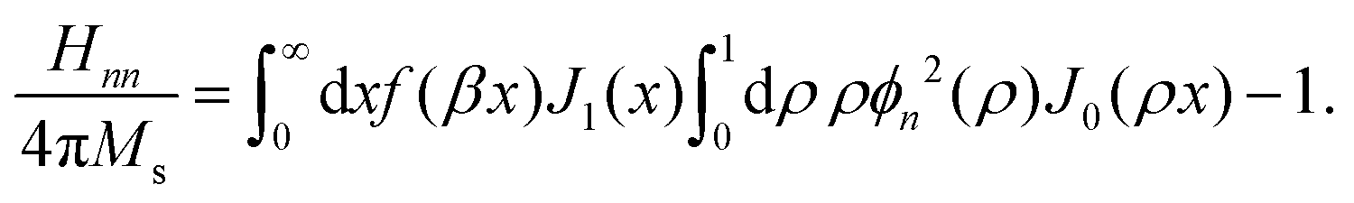 | (2) |
2.8 Micromagnetic simulations
The micromagnetic simulations were performed by using the MuMax3 solver.60 The Ms and A values were extracted from the best fits of the experimental data to the described analytical theory. The values reported in Fig. 3(c) and (d) have been used as the input parameters for the simulations. For all nanodisk radii the cell size was 2.5 × 2.5 × 2.5 nm3 and the damping parameter was α = 0.01. The simulations were performed in two stages, a static one and a dynamic one. At the first stage, an equilibrium magnetic configuration of the system was reached by relaxing a random magnetic configuration for each value of the out-of-plane bias field H from a given set. Subsequently, magnetization precession was excited by applying a small spatially uniform in-plane microwave field h ∝ sin![[thin space (1/6-em)]](https://www.rsc.org/images/entities/char_2009.gif) c(2πfcut(t − t0)), where fcut = 40 GHz is the cut-off frequency and t0 = 0.5 ns is the time delay after which the sinc function reaches its maximum. The dynamic response of the system has been recorded with the sampling interval equal to 1.25 ns. Finally, a fast Fourier transform was used to extract the normalized frequency spectra and the magnetization profiles at the resonance frequencies of the standing spin waves.61
c(2πfcut(t − t0)), where fcut = 40 GHz is the cut-off frequency and t0 = 0.5 ns is the time delay after which the sinc function reaches its maximum. The dynamic response of the system has been recorded with the sampling interval equal to 1.25 ns. Finally, a fast Fourier transform was used to extract the normalized frequency spectra and the magnetization profiles at the resonance frequencies of the standing spin waves.61
3 Results and discussion
Fig. 2(a) and (b) present the experimentally measured spin-wave resonance spectra as a function of the out-of-plane magnetic field for the disks of different radii. For all nanodisk radii, the main resonance peak is observed at the largest field (e.g., for the nanodisk with R = 1000 nm at 14 kOe) and it corresponds to the lowest spin-wave mode number n = 1, as will be detailed below. In addition to the main resonance peak there are several well-defined resonance peaks at smaller fields. The magnitude of the peaks monotonically decreases with increase of the mode number. As the disk radius decreases, the spin-wave spectra shift towards lower fields and the distance between the neighboring resonances increases.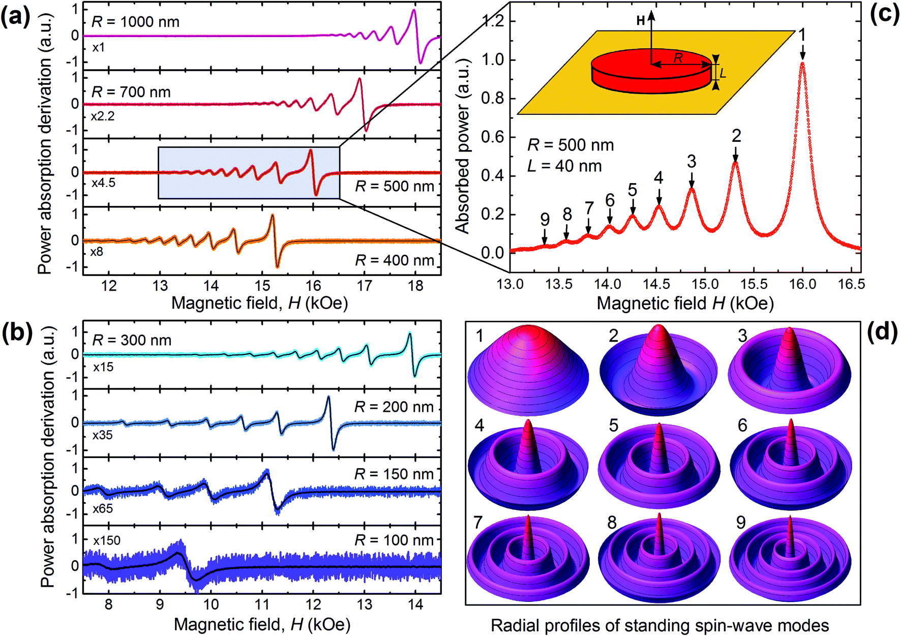 | ||
| Fig. 2 Spin-wave resonance spectra. (a) and (b) Experimentally measured spin-wave resonance spectra at 9.85 GHz for a series of 40 nm-thick CoFe-FEBID disks with different radii, as indicated. Black lines are averages of 50 neighboring points. Multiplication factors for the signals with respect to the 1 μm disk measurement are labeled close to the data. (c) Field dependence of the microwave power absorption (symbols) for the disk with a radius of 500 nm. At least nine spin-wave resonance modes can be identified, as labeled close to the peaks. Inset: Geometry used in the analytical theory. (d) Radial profiles of the first nine standing spin-wave modes described by the zeroth-order Bessel functions. | ||
Importantly, it was possible to detect the signal even for the smallest disk with a radius of only 100 nm. In previous studies, arrays consisting of 106–107 identical disks were investigated using conventional FMR spectroscopy to reach the required sensitivity. In our experiment, for the smallest nanodisk the signal-to-noise ratio (SNR) is about 2. Nevertheless, two spin-wave peaks are observable at the positions predicted by the analytical theory to be introduced in what follows. For a larger nanodisk with R = 150 nm, the SNR increases to about 5 and four spin-wave peaks can be clearly distinguished. The SNR continues to noticeably increase as the disk radius R increases, and more and more standing spin-wave modes become visible. For instance, the largest number of modes (9 modes) can be identified for the disk with R = 500 nm, as illustrated in Fig. 2(c). From the measured spin-wave spectra, for each mode n and disk radius R, the resonance fields Hres were deduced at fields at which the power absorption derivative turns into zero, which is equivalent to the definition of Hres from at the absorbed power maxima in Fig. 2(c). The deduced dependences of the spin-wave resonance fields Hres on the mode number n for different nanodisk radii are presented in Fig. 3(a).
 | ||
| Fig. 3 (a) Dependence of the resonance field Hres on the spin-wave mode number n. Symbols are experimental data. Solid lines are fits to the analytical theory with the magnetization Ms and the exchanged constant A varied as fitting parameters, as reported in panels (b) and (c), and the gyromagnetic ratio γ/2π = 3.05 MHz Oe−1. The background color gradient designates a crossover from the regime of dipolar spin waves at larger R and smaller n to the regime of dipole-exchange spin waves at smaller R and larger n. (d) Metal content in the nanodisks as inferred from energy-dispersive X-ray spectroscopy. The lines in (b), (c) and (d) are guides for the eye. The background color in (b), (c), and (d) indicates a crossover from the deposition of samples in a depleted-precursor mode (deposition mode I, yellow) to an almost precursor depletion-free mode (deposition mode II, blue) as the disk size increases. | ||
Standing spin waves appear in nanoelements because of the quantization of the radial spin-wave vector component due to the elements’ finite lateral size.56 To describe analytically the field values at which the spin-wave resonance appear, we consider azimuthally symmetric spin waves in a thin cylindrical ferromagnetic disk of thickness L and radius R saturated in the out-of-plane direction by the biasing magnetic field H, see the inset in Fig. 2(c). In the case of out-of-plane magnetized circular disks the excited spin-wave eigenmodes can be described by Bessel functions of the zeroth order because of the axial symmetry of the samples.56 For details on the analytical calculations we refer to the Methods section. The radial profiles of the first nine spin-wave modes are illustrated in Fig. 2(d).
Fitting of the experimental dependences Hres(n) in Fig. 3(a) with the use of the theoretical model allows for the deduction of the saturation magnetization Ms and the exchange stiffness A for all individual nanodisks (see Fig. 3(b) and (c)). In Fig. 3(a), solid lines are fits to the analytical theory with the magnetization Ms and the exchanged constant A varied as fitting parameters, as reported in Fig. 3(b) and (c), and the gyromagnetic ratio γ/2π = 3.05 MHz Oe−1.62 We note that the location of the main resonance peak is largely determined by Ms and the demagnetizing factor of the sample. The value of A only weakly affects the position of the main resonance peak, however, it strongly affects the positions of the higher order peaks. The deduced Ms and A values suggest that in contrast to samples prepared by electron-beam lithography, Ms of the nanoelements fabricated by FEBID significantly depends on the elements’ lateral dimensions, and even for the largest nanodisk with R = 1000 nm, the deduced Ms and A values are by about 35% and 10% smaller than the respective values for Co3Fe thin films.63
Having deduced the saturation magnetization and the exchange constant for disks with radii down to 100 nm we now turn to a discussion of the obtained results. We believe that the decrease of Ms with decrease of the disk radius is a consequence of the employed writing strategy in the FEBID process. This underlines the importance of the characterization described here for as-fabricated FEBID samples. Namely, in the FEBID process, each nanodisk was defined as a circular polygon in which the number of points for the beam to dwell is proportional to the square of the nanodisk radius. The writing of the 40 nm-thick nanodisks required a few thousands passes of the electron beam. Accordingly, given that the point-to-point distance (pitch) for all nanodisks was kept constant, a complete rastering of the beam over the smaller disks occurred faster as compared to the larger disks. Because of the finite time needed for the precursor gas to replenish in the vicinity of the sample, the smaller disks were written in the depleted-precursor regime, which results in an increase of the carbon and oxygen content at the expense of cobalt and iron. A crossover from the deposition of samples in the depleted-precursor mode (deposition mode I) to an almost precursor depletion-free mode (deposition mode II) with increase of the disk size is illustrated by the yellow-to-blue background color gradient in Fig. 3(b)–(d). We note that a decrease of Ms with decrease of the size of Co-FEBID nanospheres grown on cantilever tips was also attributed to a decrease of the metal content in the smaller spheres.64
Specifically, for the samples investigated here, the [Co + Fe] content in the nanodisks has been found to decrease from about 83 at% for the largest disk to about 58 at% for the smallest disk while the [C + O] content increased from about 17 at% to about 42 at%, see Fig. 3(d). Remarkably, the deduced Ms values in Fig. 3(b) correlate rather well with the [Co + Fe] content in Fig. 3(d) which suggests that the reduction of Ms in the samples can be attributed to the reduction of the content of the magnetic Co and Fe in the sample volume. By employing a different writing strategy in which the electron beam was “parked” for 10 ms outside of the structure after each pass to allow the precursor to replenish, Ms values close to 1350 emu cm−3 have been deduced for a reference set of samples regardless of the nanodisk size. Meanwhile, the deduced values of A(R), despite following qualitatively the behavior of Ms(R), are decreasing by only about 10% with decrease of the disk radius. In Fig. 3(c), the deduced A value for the nanodisk with R = 100 nm is not shown because only two modes were observed for this sample, that results in a relatively large error in the determination of the exchange stiffness.
Fig. 4(a) illustrates the accuracy of the fits of the experimental dependences Hres(n) to the analytical theory using the same values of Ms and A as in Fig. 3(b) and (c) in comparison with the curves for different A values. Solid lines in Fig. 4(a) correspond to the best-fit A values in Fig. 3(c) while dashed lines pertain to A values that are smaller or larger than the best-fit ones by 10%. As follows from the fits, the accuracy of the deduction of A strongly increases with reduction of the nanodisk radius. This is a consequence of the increasing role of the exchange interaction affecting the spin-wave dynamics in smaller nanodisks. In addition, the exchange interaction more strongly influences higher-order spin-wave modes. This can be understood as a consequence of the spin-wave wavelength reduction with increase of n and the associated crossover from the regime of dipolar spin waves at larger R and smaller n (with spin-wave wavelengths λ ≃ 1 μm) to the regime of dipole-exchange spin waves at smaller R and larger n (with λ ≲ 100 nm). This crossover is indicated by the background color gradient in Fig. 3(a). Specifically, in our measurements the shortest wavelengths were detected for the disks with R = 200 nm and 300 nm. The mode numbers n = 7 and n = 9, 10 detected for R = 200 nm and R = 300 nm, respectively, correspond to effective spin-wave wavelengths of λ ≃ R/n ≈ 30 nm whose properties are determined by both, the dipolar and exchange interactions.
 | ||
| Fig. 4 (a) Fits of the experimental spin wave resonance spectra for the disks with different radii using the same values of Ms and A as in Fig. 3, but also for different A values. Solid lines correspond to the best-fit A values in Fig. 3(c) while dashed lines pertain to A values that are smaller or larger than the best-fit ones by 10%. (b) Comparison of the experimental and simulated resonance fields Hres for a series of samples and resonance modes. Micromagnetic simulations were performed using MuMax3, with the saturation magnetization Ms and the exchange stiffness A as parameters deduced from the fits of the experimental data to the analytical theory in Fig. 3. | ||
The reliability of the magnetic parameters deduced from the analytical theory was additionally examined by means of micromagnetic simulations. The simulations were done using MuMax360 for four nanodisks with radii of 150, 200, 300, and 500 nm. The simulation results are presented in Fig. 4(b), where the simulated Hres values as a function of the spin-wave mode number n fit well the experimentally measured ones. The disagreement between the simulated and the experimentally measured Hres values does not exceed 3%. This means that the used analytical theory is reliable in the whole range of aspect ratios β = L/R of up to 0.4 and it can be applied for the deduction of the saturation magnetization and the exchange stiffness for nanomagnets of cylindrical shape. Remarkably, the good correspondence between the results of analytical calculations and micromagnetic simulations indicates a validity of the used analytical model going beyond the initial approximation L ≪ R used in the theoretical derivation.56 Once Ms and A are deduced, they can be further used as input parameters for simulations (see ESI Note 1, Fig. S1 and Movie 1†) which allow one to predict the response of the nanodisks at essentially higher frequencies than 9.85 GHz used just as an exemplary FMR frequency in our experiment.
Turning to the general importance of the obtained results, it is worth noting that a particular advantage of the employed standing spin-wave resonance technique in comparison with conventional magnetometry is that it is not necessary to know the mass of the sample for the deduction of its Ms. The knowledge of the geometrical dimensions of the sample is sufficient. This is, in particular, important in the case of samples fabricated by FEBID since the density of the deposits may vary depending on the deposition parameters and post-growth treatments such as annealing and irradiation with ions and electrons.15 Also, such an important parameter as the exchange stiffness can be deduced from fits of the experimental data to the analytical theory. In return, the deduced saturation magnetization and the exchange stiffness can be used as input parameters for simulations of more complex 3D nanoarchitectures.3,5,7,55 This is especially fortunate, because various complex geometries with lateral feature sizes down to 10 nm can be fabricated by FEBID, but no analytical theory is available for their description despite the few cases of simplest symmetries. In this way, due to the available analytical description allowing for precise deduction of Ms and A, circular nanodisks can be used as standard reference samples for the verification of micromagnetic simulations which, in turn, allow for modeling the magnetization dynamics in complex-shaped direct-write nanostructures for 3D nanomagnetism and magnon spintronics. In addition, the capability of FEBID to deposit magnetic layers with pre-defined properties onto conventional microwave circuits17 makes it a valuable fabrication tool for nanomagnonics requiring microwave-to-magnon transducers for excitation and detection of phase-coherent exchange magnons with λ below 50 nm.52 Finally, a modified version of the described microwave detection approach could be useful in studies of low electrical signal spin torque oscillators.65
4 Conclusions
In summary, we have demonstrated spin-wave spectroscopy of individual circular magnetic elements with radii down to 100 nm and total volumes down to 10−3 μm3. These are the smallest magnetic elements successfully probed in the presence of a uniform microwave field so far. The novelty of the presented methodology consists in the combination of spatially resolved spin-wave spectroscopy of individual magnetic elements with inductive probing using a uniform microwave field. In our approach the sample itself is acting as a multi-mode resonator, which is distinct from previous FMR works dealing with arrays of a large number of elements or probing of single nanoelements in the presence of non-uniform fields by using microresonator-based FMR. We have illustrated the use of standing spin waves as magneto-dynamical probes of nanodisks fabricated by FEBID and exhibiting a decrease of Ms with decrease of the disk radius because of a reduction of the metal content with decrease of the elements’ sizes. Up to 9 higher-order modes of spin-wave resonances have been observed and effective spin-wave wavelengths down to 30 nm have been detected. The two key ingredients of the described approach are the tapered coplanar waveguide and the circular symmetry of the nanodisks allowing the samples themselves to act as nanoresonators. Furthermore, the circular symmetry of the nanodisks has allowed for the deduction of the saturation magnetization and the exchange stiffness of the material with high precision using an analytical theory. The deduced values have been used as input parameters for micromagnetic simulations which allowed us to reproduce the experimentally measured resonance fields with an accuracy better than 3% and, hence, can be used for modeling the magnetodynamic response of complex-shaped magnetic nanoelements for which no analytical description is available. The good correspondence between the results of analytical calculations and micromagnetic simulations indicates a validity of the used analytical model going beyond the initial thin-disk approximation used in the theoretical derivation. In all, while the developed methodology can be applied to any magnetic material, it is especially valuable for the characterization of building blocks of direct-write nano-architectures for 3D nanomagnetism and magnonics.Conflicts of interest
There are no conflicts to declare.Acknowledgements
This work was supported by the European Commission in the framework of the Horizon 2020 Marie Sklodowska-Curie program–Research and Innovation Staff Exchange (MSCA-RISE) under grant agreement no. 644348 (MagIC). Further, support by the European Cooperation in Science and Technology via COST Action CA16218 (NANOCOHYBRI) is acknowledged. The Austrian team acknowledges support by the Austrian Science Fund (FWF) under grant no. I 4889 (CurviMag). The Portuguese team acknowledges the Network of Extreme Conditions Laboratories-NECL and Portuguese Foundation of Science and Technology (FCT) support through project no. NORTE-01-0145-FEDER-022096, POCI-0145-FEDER-030085 (NOVAMAG), and EXPL/IF/00541/2015. D. N. acknowledges the Spanish Ministry for Science, Innovation and Universities, for funding through the “Ramon y Cajal” program RYC-2017-22820. A. V. C. acknowledges support within the ERC Starting grant no. 678309 MagnonCircuits. M. K. and P. G. acknowledge support of National Science Center Poland under the project UMO-2018/30/Q/ST3/00416. K. Y. G. acknowledges support by IKERBASQUE (the Basque Foundation for Science) and by the Spanish Ministry of Economy and Competitiveness under the project FIS2016-78591-C3-3-R. Support through the Frankfurt Center of Electron Microscopy (FCEM) is gratefully acknowledged. Open access funding has been provided by the University of Vienna.References
- R. Streubel, F. Kronast, P. Fischer, D. Parkinson, O. G. Schmidt and D. Makarov, Nat. Commun., 2015, 6, 7612 CrossRef.
- A. Fernández-Pacheco, R. Streubel, O. Fruchart, R. Hertel, P. Fischer and R. P. Cowburn, Nat. Commun., 2017, 8, 15756 CrossRef.
- R. Winkler, J. D. Fowlkes, P. D. Rack and H. Plank, J. Appl. Phys., 2019, 125, 210901 CrossRef.
- G. Williams, M. Hunt, B. Boehm, A. May, M. Taverne, D. Ho, S. Giblin, D. Read, J. Rarity, R. Allenspach and S. Ladak, Nano Res., 2018, 11, 845–854 CrossRef.
- A. Fernandez-Pacheco, L. Skoric, J. De Teresa, J. Pablo-Navarro, M. Huth and O. V. Dobrovolskiy, Materials, 2020, 13, 3774 CrossRef CAS.
- R. Streubel, P. Fischer, F. Kronast, V. P. Kravchuk, D. D. Sheka, Y. Gaididei, O. G. Schmidt and D. Makarov, J. Phys. D, 2016, 49, 363001 CrossRef.
- L. Skoric, D. Sanz-Hernández, F. Meng, C. Donnelly, S. Merino-Aceituno and A. Fernández-Pacheco, Nano Lett., 2020, 20, 184–191 CrossRef CAS.
- Three-Dimensional Magnonics: Layered, Micro- and Nanostructures, ed. G. Gubbiotti, Jenny Stanford Publishing, 2019 Search PubMed.
- O. V. Dobrovolskiy, R. Sachser, T. Brächer, T. Böttcher, V. V. Kruglyak, R. V. Vovk, V. A. Shklovskij, M. Huth, B. Hillebrands and A. V. Chumak, Nat. Phys., 2019, 15, 477 Search PubMed.
- O. V. Dobrovolskiy, Physica C, 2017, 533, 80–90 CrossRef CAS.
- F. Porrati, S. Barth, R. Sachser, O. V. Dobrovolskiy, A. Seybert, A. S. Frangakis and M. Huth, ACS Nano, 2019, 13, 6287–6296 CrossRef CAS.
- A. Lara, O. V. Dobrovolskiy, J. L. Prieto, M. Huth and F. G. Aliev, Appl. Phys. Lett., 2014, 105, 182402 CrossRef.
- O. V. Dobrovolskiy, R. Sachser, S. A. Bunyaev, D. Navas, V. M. Bevz, M. Zelent, W. Smigaj, J. Rychly, M. Krawczyk, R. V. Vovk, M. Huth and G. N. Kakazei, ACS Appl. Mater. Interfaces, 2019, 11, 17654 CrossRef CAS.
- L. Flajšman, K. Wagner, M. Vaňatka, J. Gloss, V. Křižáková, M. Schmid, H. Schultheiss and M. Urbánek, Phys. Rev. B, 2020, 101, 014436 CrossRef.
- O. V. Dobrovolskiy, M. Kompaniiets, R. Sachser, F. Porrati, C. Gspan, H. Plank and M. Huth, Beilstein J. Nanotechnol., 2015, 6, 1082–1090 CrossRef CAS.
- O. V. Dobrovolskiy, E. Begun, M. Huth, V. A. Shklovskij and M. I. Tsindlekht, Physica C, 2011, 471, 449–452 CrossRef CAS.
- O. V. Dobrovolskiy, V. M. Bevz, E. Begun, R. Sachser, R. V. Vovk and M. Huth, Phys. Rev. Appl., 2019, 11, 054064 CrossRef CAS.
- M. Kompaniiets, O. V. Dobrovolskiy, C. Neetzel, F. Porrati, J. Brötz, W. Ensinger and M. Huth, Appl. Phys. Lett., 2014, 104, 052603 CrossRef.
- A. S. Mel'nikov and A. I. Buzdin, Phys. Rev. Lett., 2016, 117, 077001 CrossRef.
- M. Krawczyk and D. Grundler, J. Phys.: Condens. Matter, 2014, 26, 123202 CrossRef CAS.
- A. V. Chumak, A. A. Serga and B. Hillebrands, J. Phys. D: Appl. Phys., 2017, 50, 244001 CrossRef.
- E. N. Beginin, A. V. Sadovnikov, A. Y. Sharaevskaya, A. I. Stognij and S. A. Nikitov, Appl. Phys. Lett., 2018, 112, 122404 CrossRef.
- C. S. Davies, A. Francis, A. V. Sadovnikov, S. V. Chertopalov, M. T. Bryan, S. V. Grishin, D. A. Allwood, Y. P. Sharaevskii, S. A. Nikitov and V. V. Kruglyak, Phys. Rev. B: Condens. Matter Mater. Phys., 2015, 92, 020408 CrossRef.
- T. Sebastian, K. Schultheiss, B. Obry, B. Hillebrands and H. Schultheiss, Front. Phys., 2015, 3, 35 Search PubMed.
- N. O. Urs, B. Mozooni, P. Mazalski, M. Kustov, P. Hayes, S. Deldar, E. Quandt and J. McCord, AIP Adv., 2016, 6, 055605 CrossRef.
- J. Jersch, V. E. Demidov, H. Fuchs, K. Rott, P. Krzysteczko, J. Münchenberger, G. Reiss and S. O. Demokritov, Appl. Phys. Lett., 2010, 97, 152502 CrossRef.
- V. Sluka, T. Schneider, R. A. Gallardo, A. Kákay, M. Weigand, T. Warnatz, R. Mattheis, A. Roldán-Molina, P. Landeros, V. Tiberkevich, A. Slavin, G. Schütz, A. Erbe, A. Deac, J. Lindner, J. Raabe, J. Fassbender and S. Wintz, Nat. Nanotechnol., 2019, 14, 328–333 CrossRef CAS.
- Y. Guang, I. Bykova, Y. Liu, G. Yu, E. Goering, M. Weigand, J. Gräfe, S. K. Kim, J. Zhang, H. Zhang, Z. Yan, C. Wan, J. Feng, X. Wang, C. Guo, H. Wei, Y. Peng, Y. Tserkovnyak, G. Han and X. Schütz, Nat. Commun., 2020, 11, 949 CrossRef CAS.
- M. Farle, Rep. Prog. Phys., 1998, 61, 755–826 CrossRef CAS.
- B. Heinrich, Z. Celinski, J. F. Cochran, A. S. Arrott and K. Myrtle, J. Appl. Phys., 1991, 70, 5769–5774 CrossRef CAS.
- S. S. Kalarickal, P. Krivosik, M. Wu, C. E. Patton, M. L. Schneider, P. Kabos, T. J. Silva and J. P. Nibarger, J. Appl. Phys., 2006, 99, 093909 CrossRef.
- G. N. Kakazei, Y. G. Pogorelov, M. D. Costa, T. Mewes, P. E. Wigen, P. C. Hammel, V. O. Golub, T. Okuno and V. Novosad, Phys. Rev. B: Condens. Matter Mater. Phys., 2006, 74, 060406 CrossRef.
- C. P. Poole, Electron Spin Resonance - A Comprehensive Treatise on Experimental Techniques, John Wiley & Sons, New York, London, Sydney, 2nd edn, 1983 Search PubMed.
- F. G. Aliev, J. F. Sierra, A. A. Awad, G. N. Kakazei, D.-S. Han, S.-K. Kim, V. Metlushko, B. Ilic and K. Y. Guslienko, Phys. Rev. B: Condens. Matter Mater. Phys., 2009, 79, 174433 CrossRef.
- X. Zhou, D. Kumar, I. S. Maksymov, M. Kostylev and A. O. Adeyeye, Phys. Rev. B: Condens. Matter Mater. Phys., 2015, 92, 054401 CrossRef.
- H. T. Nembach, J. M. Shaw, C. T. Boone and T. J. Silva, Phys. Rev. Lett., 2013, 110, 117201 CrossRef.
- S. Tamaru, K. Yakushiji, A. Fukushima, S. Yuasa and H. Kubota, IEEE Magn. Lett., 2014, 5, 1–4 CAS.
- C. J. Safranski, Y.-J. Chen, I. N. Krivorotov and J. Z. Sun, Appl. Phys. Lett., 2016, 109, 132408 CrossRef.
- Z. Zhang, P. C. Hammel and P. E. Wigen, Appl. Phys. Lett., 1996, 68, 2005–2007 CrossRef CAS.
- G. De Loubens, A. Riegler, B. Pigeau, F. Lochner, F. Boust, K. Y. Guslienko, H. Hurdequint, L. W. Molenkamp, G. Schmidt, A. N. Slavin, V. S. Tiberkevich, N. Vukadinovic and O. Klein, Phys. Rev. Lett., 2009, 102, 177602 CrossRef CAS.
- F. Guo, L. M. Belova and R. D. McMichael, Phys. Rev. Lett., 2013, 110, 017601 CrossRef.
- R. Adur, C. Du, H. Wang, S. A. Manuilov, V. P. Bhallamudi, C. Zhang, D. V. Pelekhov, F. Yang and P. C. Hammel, Phys. Rev. Lett., 2014, 113, 176601 CrossRef.
- M. Möller, K. Lenz and J. Lindner, J. Surf. Interf. Mater., 2014, 2, 46–68 Search PubMed.
- T. Schaffers, R. Meckenstock, D. Spoddig, T. Feggeler, K. Ollefs, C. Schöppner, S. Bonetti, H. Ohldag, M. Farle and A. Ney, Rev. Sci. Instrum., 2017, 88, 093703 CrossRef CAS.
- K. Lenz, R. Narkowicz, K. Wagner, C. F. Reiche, J. Körner, T. Schneider, A. Kákay, H. Schultheiss, D. Weissker, U. Wolf, D. Suter, B. Büchner, J. Fassbender, T. Mühl and J. Lindner, Small, 2019, 15, 1904315 CrossRef CAS.
- A. A. Serga, A. V. Chumak and B. Hillebrands, J. Phys. D: Appl. Phys., 2010, 43, 264002 CrossRef.
- D. M. Pozar, Microwave engineering, John Wiley & Sons, Inc., New York, 4th edn, 2011 Search PubMed.
- B. Hillebrands and K. Ounadjela, Spin Dynamics in Confined Magnetic Structures I, Springer-Verlag, New York, NY, USA, 2002 Search PubMed.
- D. D. Stancil and A. Prabhakar, Spin Waves. Theory and Applications, Springer, Berlin, 2009 Search PubMed.
- D. Grundler, Nat. Nanotechnol., 2016, 11, 407 CrossRef CAS.
- H. Yu, O. d'Allivy Kelly, V. Cros, R. Bernard, P. Bortolotti, A. Anane, F. Brandl, F. Heimbach and D. Grundler, Nat. Commun., 2016, 7, 11255 CrossRef CAS.
- P. Che, K. Baumgaertl, A. Kúkol'ová, C. Dubs and D. Grundler, Nat. Commun., 2020, 11, 1445 CrossRef CAS.
- T. P. R. Kumar, I. Unlu, S. Barth, O. Ingólfsson and D. H. Fairbrother, J. Phys. Chem. C, 2018, 122, 2648–2660 CrossRef.
- F. Porrati, M. Pohlit, J. Müller, S. Barth, F. Biegger, C. Gspan, H. Plank and M. Huth, Nanotechnology, 2015, 26, 475701 CrossRef CAS.
- L. Keller, M. K. I. Al Mamoori, J. Pieper, C. Gspan, I. Stockem, C. Schröder, S. Barth, R. Winkler, H. Plank, M. Pohlit, J. Müller and M. Huth, Sci. Rep., 2018, 8, 6160 CrossRef.
- G. N. Kakazei, P. E. Wigen, K. Y. Guslienko, V. Novosad, A. N. Slavin, V. O. Golub, N. A. Lesnik and Y. Otani, Appl. Phys. Lett., 2004, 85, 443–445 CrossRef CAS.
- B. A. Kalinikos and A. N. Slavin, J. Phys. C, 1986, 19, 7013 CrossRef.
- K. Y. Guslienko and A. N. Slavin, Phys. Rev. B: Condens. Matter Mater. Phys., 2005, 72, 014463 CrossRef.
- G. N. Kakazei, G. R. Aranda, S. A. Bunyaev, V. O. Golub, E. V. Tartakovskaya, A. V. Chumak, A. A. Serga, B. Hillebrands and K. Y. Guslienko, Phys. Rev. B: Condens. Matter Mater. Phys., 2012, 86, 054419 CrossRef.
- A. Vansteenkiste, J. Leliaert, M. Dvornik, M. Helsen, F. Garcia-Sanchez and B. Van Waeyenberge, AIP Adv., 2014, 4, 107133 CrossRef.
- P. Gruszecki and M. Krawczyk, Wiley Encyclop. Electr. Electron. Engineer., 2016, 1–23 Search PubMed.
- M. Tokac, S. A. Bunyaev, G. N. Kakazei, D. S. Schmool, D. Atkinson and A. T. Hindmarch, Phys. Rev. Lett., 2015, 115, 056601 CrossRef CAS.
- M. A. W. Schoen, J. Lucassen, H. T. Nembach, T. J. Silva, B. Koopmans, C. H. Back and J. M. Shaw, Phys. Rev. B, 2017, 95, 134410 CrossRef.
- S. Sangiao, C. Magen, D. Mofakhami, G. de Loubens and J. M. De Teresa, Beilstein J. Nanotechnol., 2017, 8, 2106–2115 CrossRef CAS.
- M. Collet, X. de Milly, O. d'Allivy Kelly, V. V. Naletov, R. Bernard, P. Bortolotti, J. Ben Youssef, V. E. Demidov, S. O. Demokritov, J. L. Prieto, M. Muñoz, V. Cros, A. Anane, G. de Loubens and O. Klein, Nat. Commun., 2016, 7, 10377 CrossRef CAS.
- I. Lee, Y. Obukhov, G. Xiang, A. Hauser, F. Yang, P. Banerjee, D. V. Pelekhov and P. C. Hammel, Nature, 2010, 466, 845 CrossRef CAS.
Footnote |
| † Electronic supplementary information (ESI) available: Supporting Note 1, Fig. S1, and animation 1. See DOI: 10.1039/D0NR07015G |
| This journal is © The Royal Society of Chemistry 2020 |