
 Open Access Article
 This Open Access Article is licensed under a
 Creative Commons Attribution 3.0 Unported Licence
Self-assembled nanodisks in coaxial GaAs/GaAsBi/GaAs core–multishell nanowires†
Bin
Zhang
 a,
Mattias
Jansson
a,
Yumiko
Shimizu
b,
Weimin M.
Chen
a,
Fumitaro
Ishikawa
*c and
Irina A.
Buyanova
*a
a,
Mattias
Jansson
a,
Yumiko
Shimizu
b,
Weimin M.
Chen
a,
Fumitaro
Ishikawa
*c and
Irina A.
Buyanova
*a
aDepartment of Physics, Chemistry and Biology, Linköping University, 581 83 Linköping, Sweden. E-mail: irina.bouianova@liu.se
bToray Research Center, 3-3-7 Sonoyama, Otsu, Shiga 520-8567, Japan
cGraduate School of Science and Engineering, Ehime University, Ehime 790-8577, Matsuyama, Japan. E-mail: ishikawa.fumitaro.zc@ehime-u.ac.jp
First published on 8th October 2020
Abstract
III–V semiconductor nanowires (NWs), such as those based on GaAs, are attractive for advanced optoelectronic and nanophotonic applications. The addition of Bi into GaAs offers a new avenue to enhance the near-infrared device performance and to add new functionalities, by utilizing the remarkable valence band structure and the giant bowing in the bandgap energy. Here, we report that alloying with Bi also induces the formation of optically-active self-assembled nanodisks caused by Bi segregation. They are located in the vicinity to the 〈112〉 corners of the GaAsBi shell and are restricted to twin planes. Furthermore, the Bi composition in the disks is found to correlate with their lateral thickness. The higher Bi composition in the disks with respect to the surrounding matrix provides a strong confinement for excitons along the NW axis, giving rise to narrow emission lines (<450 μeV) with the predominant emission polarization orthogonal to the NW axis. Our findings, therefore, open a new possibility to fabricate self-assembled quantum structures by combining advantages of dilute bismide alloys and lattice engineering in nanowires.
III–V semiconductor nanowires (NWs), e.g. those based on GaAs, have been a central focus of research because of their scientific importance and promising technological applications in the area of nanoelectronics and optoelectronics.1 Indeed, the quasi one-dimensional (1D) architecture and a small foot print allow NW growth on foreign substrates, which can be utilized for integration of III–V NWs with excellent optical and transport properties into Si-based microelectronic circuits and devices.2 The ability to grow NWs as ordered arrays is crucial for boosting efficiency of optical absorption and solar energy harvesting above that achievable in thin films.3 The nanowire itself also provides a naturally-formed cavity/waveguide and an active gain medium, which favors effective light extraction and is highly desirable for advanced photonic devices, including next-generation lasers4–9 and photodetectors.10
Currently, there is a considerable interest in extending the bandgap of III–V-based NWs towards the infrared range of 1.3–1.55 μm required for fiber-optic communications. For these purposes, ternary GaAsBi NWs are considered to be among the most promising materials owing to attractive changes in the electronic structure upon Bi incorporation.11 The giant bandgap bowing and a strong perturbation of valence band (VB) states in this highly mismatched semiconductor alloy12,13 lead to wide bandgap tunability via tuning Bi content, so that a drastic reduction in the bandgap energy (Eg) by ∼90 meV can be achieved by adding only 1% Bi into GaAs.13,14 Moreover, an enhanced spin–orbit splitting (ΔSO) enables realization of the condition Eg < ΔSO with a sufficiently high Bi concentration, which helps to restrain unwanted Auger recombination.15–18 Recently, it has been demonstrated that GaAsBi-based NWs can be synthesized as radial19,20 and axial21 heterostructures and also with both zinc blende (ZB)19–21 and wurtzite crystal structures.22 These polytypes were found to have significantly modified VB states,22 which provides a new avenue to modulate the electronic structure and, therefore, renders the GaAsBi NW system as a novel palette for the bandgap and photonic engineering.
The use of ternary compounds, however, is typically accompanied by complicated alloy fluctuations23,24 and even self-induced compositional gradient along the growth direction due to phase separation.25 Local changes in the composition necessarily cause spatial variations in the electronic structure and, therefore, the formation of a localization potential within nanowires. Though somewhat detrimental for transport properties, the localization effects create new possibilities for fabrication of self-assembled nanostructures. For example, the formation of embedded nanostructures because of alloy phase segregation were commonly observed in ternary III–V NWs, including AlGaAs,26–30 AlInP31 and GaAsP.32,33 Such self-assembled nanostructures create an exciton confinement potential and, therefore, act as optically-active quantum disks and quantum dots.26,28,34 This extends possible applications of the NW structures to e.g. future quantum information technologies.35,36 The alloy fluctuations are known to be especially pronounced in highly-mismatched alloys (e.g. GaAsBi and GaNAs), strongly magnified due to the giant bowing in the bandgap energy. In GaNAs(P) NWs, short-range fluctuations in the alloy composition act as embedded QDs with a preferential direction of the high-symmetry axis defined by the host matrix.37–39 In the case of GaBiAs NWs, Bi segregation at the {112}B surface resulting in the formation of the branched structure at azimuthal 〈112〉 direction was recently reported.20 However, no information is available so far regarding formation of optically-active self-assembled nanostructures in GaAsBi NWs. If present, it would widen the range of possible applications of this novel material system in future nanophotonic and optoelectronic devices.
This work demonstrates spontaneous formation of optically-active Bi-rich quantum disks in GaAs/GaAsBi/GaAs core–multishell NWs. Through detailed cross-sectional structural and compositional characterization, we show that the nanodisks are formed due to Bi segregation in twin planes near six 〈112〉 corners of the GaAsBi shell, which is likely driven by favorable strain relaxation. The formed nanostructures induce a strong confinement potential, giving rise to sharp emission lines with a preferential polarization. A strong correlation between lateral confinement and Bi composition is also revealed by magneto-photoluminescence (PL) measurements and an analysis of a temperature-dependent PL linewidth.
Fig. 1 overviews structural properties of the studied ZB GaAs/GaAsBi/GaAs core–multishell NWs that were grown by Ga-catalyzed molecular beam epitaxy (MBE) on phosphorus-doped n-type Si (111) substrates (see Methods for a more detailed description of the NW growth). The NWs have corrugated surface morphology induced by the presence of Bi,19,20 as can be seen from representative scanning electron microscopy (SEM) and scanning transmission electron microscopy (STEM) images shown in Fig. 1(a). The wires appear to be straight, which suggests that the surface modulation occurred at the shell layer, and the inside core was formed with a straight structure. The upper part of Fig. 1(b) shows a zoomed-in radial cross-sectional bright field (BF) STEM image of the wire observed from the [11![[2 with combining macron]](https://www.rsc.org/images/entities/char_0032_0304.gif) ] direction, confirming the intended GaAs/GaAsBi/GaAs core/shell/shell heterostructure, where the inner GaAsBi shell can be recognized by its darker contrast. (The GaAs/GaAsBi/GaAs core/shell/shell regions are demarcated by vertical dashed lines for easier visualization.) All the layers are found to be approximately 70 nm wide, which is further confirmed by the microscopic studies of the NW axial cross-section to be discussed below. In addition to the multishell structure, we also observe dark radial bands that propagate through the GaAsBi shell. From the radial cross-sectional BF-STEM images (Fig. 1(b)), these dark structures are elongated in the horizontal direction with a length of ∼70 nm and a width varying between one and several tens of nanometers. This can also be seen from the lower part of Fig. 1(b), where the magnified BF-STEM image of the delimited area in the upper part of Fig. 1(b) is shown.
] direction, confirming the intended GaAs/GaAsBi/GaAs core/shell/shell heterostructure, where the inner GaAsBi shell can be recognized by its darker contrast. (The GaAs/GaAsBi/GaAs core/shell/shell regions are demarcated by vertical dashed lines for easier visualization.) All the layers are found to be approximately 70 nm wide, which is further confirmed by the microscopic studies of the NW axial cross-section to be discussed below. In addition to the multishell structure, we also observe dark radial bands that propagate through the GaAsBi shell. From the radial cross-sectional BF-STEM images (Fig. 1(b)), these dark structures are elongated in the horizontal direction with a length of ∼70 nm and a width varying between one and several tens of nanometers. This can also be seen from the lower part of Fig. 1(b), where the magnified BF-STEM image of the delimited area in the upper part of Fig. 1(b) is shown.
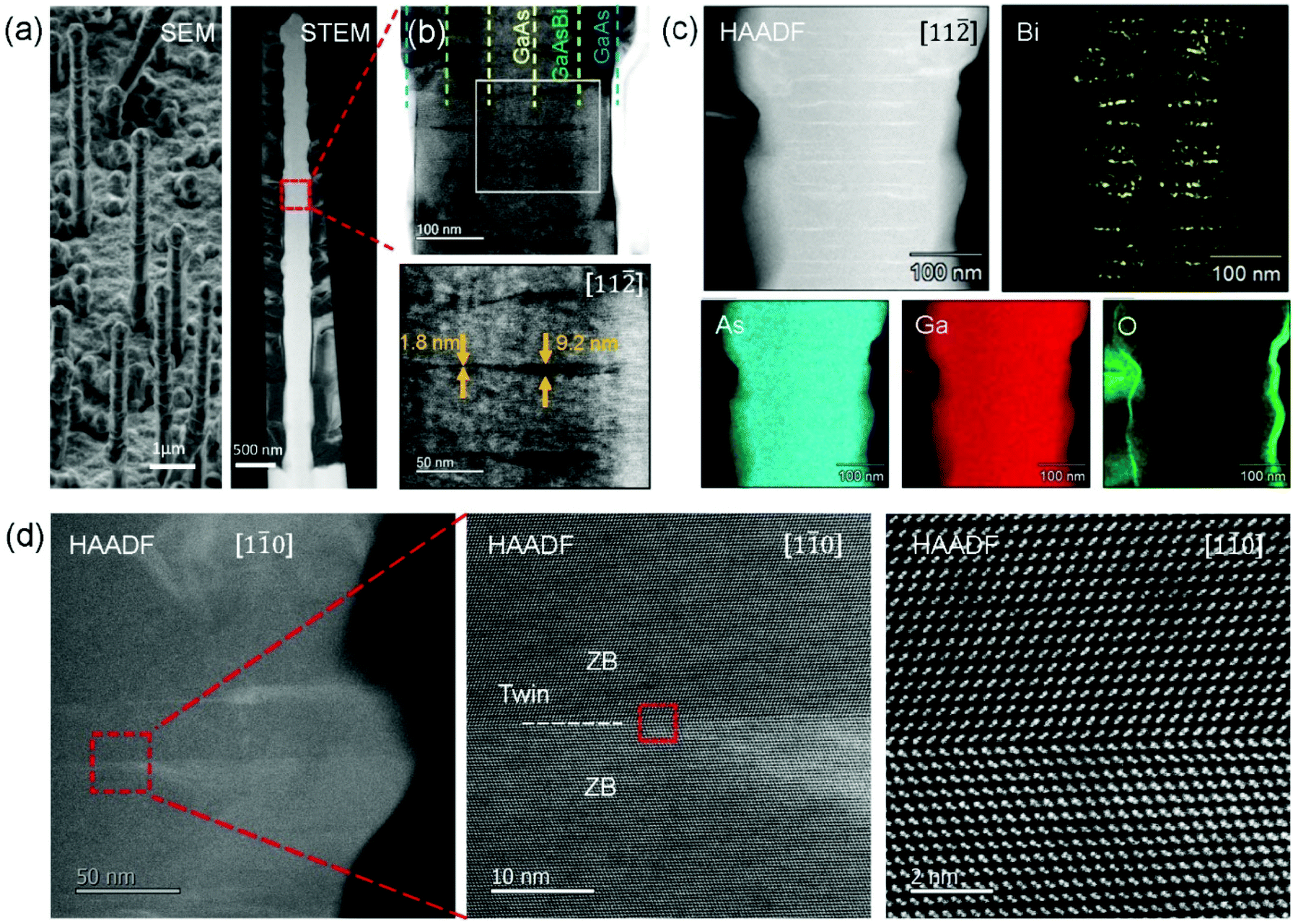 | ||
Fig. 1 (a) 45°-Tilted SEM image of the NW array (left) and a radial cross-sectional HAADF-STEM image of a single NW (right). (b) The upper panel: enlarged radial cross-sectional BF-STEM images taken in the (11) cross-section of the middle part of the NW that is delimited by the dashed rectangle shown in the right panel of (a); the lower panel: high-magnification radial cross-sectional BF-STEM image of the area marked by the solid rectangle in the upper panel. (c) Radial cross-sectional HAADF-STEM and EDS elemental mapping of Bi, As, Ga, and O performed within the same area of the NW as shown in the upper panel of (b). (d) HAADF-STEM images taken in the (1![[1 with combining macron]](https://www.rsc.org/images/entities/char_0031_0304.gif) 0) cross-section. The enlarged part of the left panel, displayed in the central part of (d), shows that the light stripe due to Bi segregation corresponds to the twin defect. The atomically resolved image of this twin defect delimited by red dashed rectangle is shown on the right panel. 0) cross-section. The enlarged part of the left panel, displayed in the central part of (d), shows that the light stripe due to Bi segregation corresponds to the twin defect. The atomically resolved image of this twin defect delimited by red dashed rectangle is shown on the right panel. | ||
To gain further information on a chemical composition of the revealed nanostructures, radial cross-sectional high-angle annular dark-field STEM (HAADF-STEM) and energy disperse spectroscopy (EDS) measurements in the middle of the NW were carried out. The corresponding results are summarized in Fig. 1(c). As the intensity of STEM images acquired in the HAADF mode is proportional to Zn (Z-contrast, here Z is the atomic number and n is typically between 1 and 2),29 the atom with a higher atomic number will exhibit brighter contrast. In our case, a Bi atom is much heavier than both Ga and As atoms. Hence the light stripes shown in Fig. 1(c) indicate accumulation of the heavy Bi atoms within the nanostructures revealed by BF-STEM (Fig. 1(b)). These results are further supported by the EDS elemental mapping. Careful inspection shows that these nanostructures are defined by thin rotational twin planes that also extend into the ZB GaAs core region, as verified by our high resolution (HR) HAADF results (see Fig. 1(d)). The twin formation is not surprising, since it requires very little energy and occurs frequently in GaAs NWs.40–42
The formation of Bi-rich nanostructures is further confirmed from the performed axial cross-sectional BF- and HAADF-STEM measurements. The corresponding results are shown in Fig. 2(a) and (b), respectively, where the GaBiAs shell can be easily distinguished by the bright contrast in the HAADF image in Fig. 2(b). The diffraction pattern in Fig. 2(e) taken from the core along the [111] direction clearly shows that the investigated NW has a hexagonal cross-section with {110} sidewall facets. Moreover, a variation of bright contrast within the GaBiAs shell is observed (Fig. 2(b)). This implies that Bi composition is higher within the corner regions of the GaBiAs shell and also differs between the adjacent 〈112〉 corners alternating between more and less elongated, as shown by the dashed contours in Fig. 2(b). This is also confirmed by the EDS elemental mapping, which is shown in Fig. 2(c) and is superimposed on the HAADF-STEM image in Fig. 2(d). In our recent study (ref. 20) we have shown that Bi preferentially incorporates along 〈112〉B directions. This could be caused by the surface configuration at the growth front, where As-rich {112}B surfaces with a higher surface energy are exposed, promoting Bi incorporation into the layer.43–45 Hence, we suggest that larger Bi accumulation occurs at the 〈112〉B corners of the GaBiAs shell.
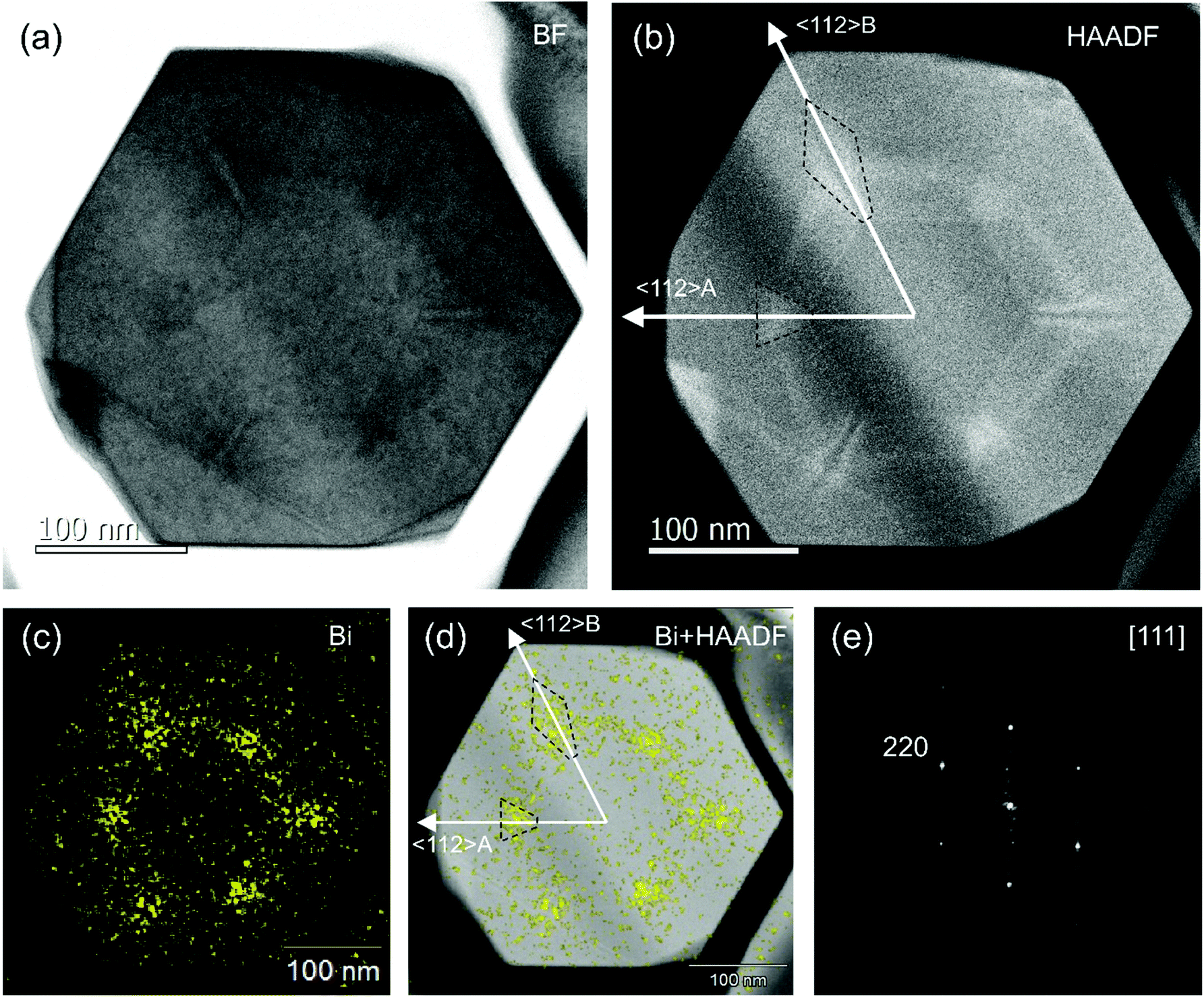 | ||
| Fig. 2 (a, b) Axial cross-sectional BF- and HAADF-STEM images of the GaAs/GaBiAs/GaAs core/shell/shell NW. (c) EDS elemental mapping of Bi performed within the same area of NW as shown in (a, b). (d) Axial cross-sectional HAADF image superimposed with Bi elemental mapping. The dashed contours in (b) and (d) highlight differences in the Bi distribution between the 〈112〉 A and 〈112〉 B corners of the GaBiAs shell. (e) Diffraction pattern taken from the core in the axial cross-section. | ||
Considering that Bi predominantly segregates within the 〈112〉 corners of the GaAsBi shell and the segregation occurs at the rotational twin planes, we conclude that the Bi-rich nanodisks with their normal vector directed along the NWs axis are formed in the GaAsBi shell region. Segregation of Bi is known in GaAsBi alloys20,46–48 and occurs to minimize the strain energy caused by the large difference in atomic size between Bi and host atoms. We suggest that in the studied NWs the formation of the Bi-rich regions in the vicinity of the 〈112〉 corners is likely favorable for misfit strain relaxation.49,50 Such segregation was previously found to be responsible for branching of GaAsBi NWs.20 Differences in the Bi distribution between two alternating 〈112〉 corners also implies that crystal polarity may play a role in such phase segregation process.33,51 Furthermore, our results suggest that the segregation of Bi is promoted at twin planes. Similar tendencies of metal impurities have been reported previously. For example, preferential accumulation of Zn at twin plane boundaries was previously demonstrated in GaAs NWs.52 It was also shown that in Si NWs metal impurity atoms first uniformly incorporate into the NWs and then redistribute and segregate at nearby defect sites, such as twin planes and stacking faults.53
To understand how the Bi segregation affects the electronic structure and optical properties of the NWs, low-temperature μ-PL measurements were performed on individual NWs transferred onto a gold-coated silica substrate. As can be seen from Fig. 3(a), the PL signal at T = 5 K is distributed within a large energy range of 1.15 to 1.32 eV and includes a series of sharp lines with a full width at half maximum (FWHM) ranging between 150 and 450 μeV. The exact spectral positions of these lines vary among different NWs and also between different spatial regions of the same NW. Their energies are much lower than those of reported emissions in GaAs NWs37,54–56 and also of PL emissions in our reference GaAs NWs, suggesting that the sharp PL lines stem from the GaAsBi shell. Taking into account a large number of the detected emissions and their narrow linewidth, we suggest that these sharp PL lines stem from the Bi-rich nanodisks revealed by TEM, where combined effects of a strong upward movement of the VB maximum and a slight downward shift of the conduction band minimum create a confinement potential for excitons. The evolution of the PL spectra with increasing excitation power (Pexc) provides additional information on their origin. As an example, Fig. 3(b) shows a series of the PL spectra taken from a representative emission line of 1.2441 eV under various Pexc. With increasing excitation power, the emission intensity of the 1.2441 eV line varies nearly linearly before approaching a saturation plateau, characteristic for neutral exciton (X) recombination. An additional low-energy emission line located at 1.2410 eV appears when the excitation power exceeds P = 14P0 (P0 = 50 nW μm−2 denotes the minimal excitation power density used during the measurements), and its intensity increases quadratically with Pexc (see also the inset of Fig. 3(b)). Consequently, this emission line dominates the PL spectra under the high excitation powers exceeding 95P0. This behavior is typical for biexcitons (XX). The corresponding binding energy can then be estimated as EbXX = 3.078 meV, which is similar to the reported values in GaAs-based QDs.57,58 (Weak shoulders on the high- and low-energy sides of the exciton and biexciton lines, respectively, are believed to originate from another nanostructure.) The values of the confinement potential can be estimated from temperature-dependent PL measurements. All PL lines are found to quench with increasing temperature (T) and can no longer be detected when T > 45 K. The activation (ionization) energy for individual lines was determined by fitting their PL intensity using the Arrhenius equation, as shown in the inset in Fig. 3(c). The obtained activation energies range between 2 and 30 meV, which is consistent with the values of spontaneously formed QDs in GaAsN38 and AlGaAs28 NWs due to short-range alloy fluctuations.
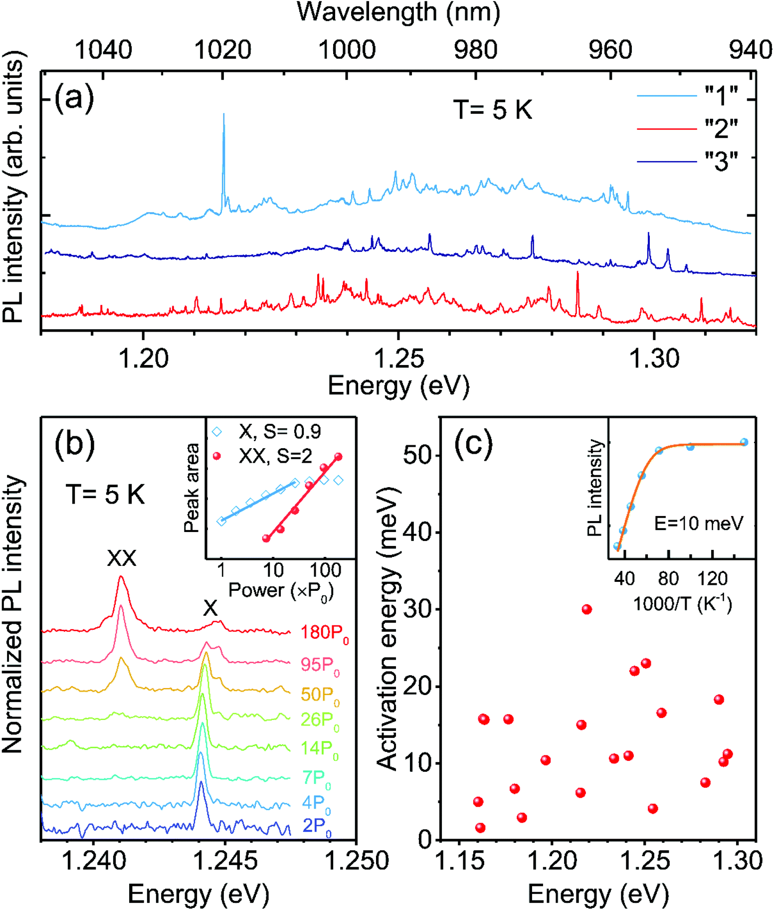 | ||
| Fig. 3 (a) Representative μ-PL spectra acquired at T = 5 K from three single GaAsBi NWs. (b) Evolution of the PL spectra with increasing excitation power density (P), where P0 = 50 nW μm−2. The inset shows integrated intensities (I) of the exciton (X) and biexciton (XX) lines as a function of P (symbols). The solid lines are the best fit to the data using the power function I ∝ PS. (c) Activation energies of the PL thermal quenching for a series of emission lines with various energies. The inset depicts temperature-dependent PL intensity from a typical line (symbols). The solid line is the best fit to the experimental data by the Arrhenius equation. | ||
As seen from Fig. 1(b–d), the Bi-rich nanostructures likely experience a strong confinement potential in the direction along the NWs axis, which can affect the electronic structure of excitons and, therefore, their optical emission properties. To gain more insight into the electronic structure of the self-assembled nanostructures, polarization-resolved PL measurements were carried out on a single NW. The used excitation power was low enough to ensure that all sharp emission lines arise from recombination of neutral excitons. Representative PL spectra detected at various azimuthal angle φ are shown in Fig. 4(a), whereas polar plots of these emissions are shown in Fig. 4(b). φ is defined as the azimuthal angle of linear polarization analyzer with respect to the NW axis (see also Fig. 4(c)). The emission intensity of an individual line as a function of φ can be fitted by the following relation:
I = Imax![[thin space (1/6-em)]](https://www.rsc.org/images/entities/char_2009.gif) cos2(φ − θ) + Iminsin2(φ − θ). cos2(φ − θ) + Iminsin2(φ − θ). | (1) |
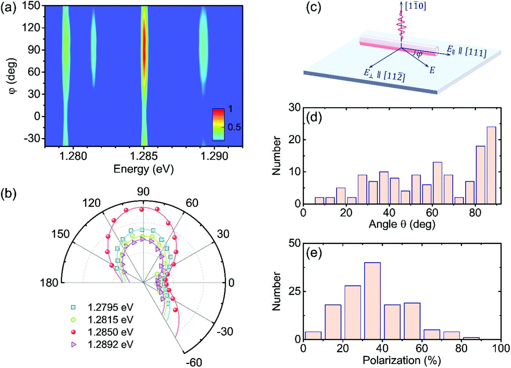 | ||
| Fig. 4 (a) Intensity of the PL emission from a single GaAsBi NW as a function of the analyzer angle φ and detection energy. (b) Polar plots of the PL intensity for several emission lines shown in (a). The solid lines are simulation results by a Malus's law equation with the polarization angle θ = 90° ± 2°. (c) Schematic illustration of the experimental configuration for polarization-resolved μ-PL measurements. E denotes the polarization direction of the linear analyzer, whereas φ is its angular position with respect to the NW axis. E∥(E⊥) is a component of E parallel (perpendicular) to the NW axis. Statistical distributions of the polarization angle θ (d) and the polarization degree P (e) of the nanodisk emissions. | ||
Here θ denotes the azimuthal angle at which the PL intensity reaches its maximum (to be referred to below as the polarization angle). The corresponding polarization degree can be calculated by P = (Imax − Imin)/(Imax + Imin) × 100%. A statistical analysis of the polarization angle and the polarization degree from a series of sharp lines are shown in Fig. 4(d) and (e) respectively. From Fig. 4(d), the statistical distribution has a clear maximum at θ = 80–90 deg. Such preferred polarization direction is typical for an exciton with a predominantly heavy-hole character that is confined in the potential with the principal quantization direction along the NW axis,38 corresponding to the orientation of the nanodisks seen in Fig. 1. Besides this set of orthogonally polarized emission lines, a wide spread of the polarization angles for other emission lines is also apparent from Fig. 4(d). This observation indicates tilting of the principal quantization axis away from the NW axis for these nanodisks due to other factors, e.g. local strain of a random orientation, consistent with the previous findings for self-assembled quantum structures in III–V nanowires.26,28
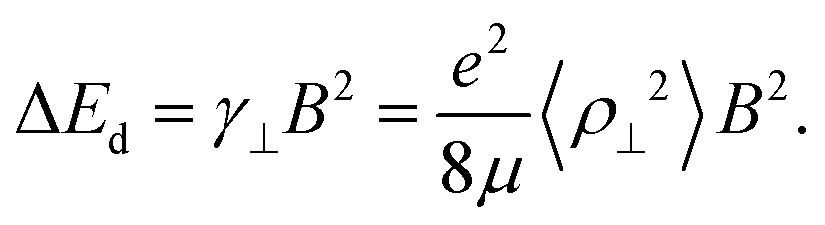
In order to evaluate an extent of exciton localization within the revealed nanostructures, we have performed magneto-PL measurements. For the vast majority of the lines, though no splitting in applied magnetic fields could be resolved, the lines are found to shift to higher energies to a variable extent. In the weak-field limit, the energy variation of a confined exciton in an applied magnetic field is dominated by the quadratic diamagnetic shift, defined as:59
 | (2) |
Here γ⊥ is the diamagnetic coefficient, whereas μ and 〈ρ⊥2〉 denote the exciton reduced mass and the extension of exciton wavefunction (thus lateral confinement) in the plane perpendicular to the magnetic field (B), respectively. Typical magneto-PL spectra acquired at various applied fields are shown in Fig. 5(a), with B∥[10] parallel to the optical excitation and detection direction. Evidently, the peak energy of the emission line shifts to higher energies with increasing B. For all the monitored PL lines, no apparent Zeeman splitting was observed. This is expected for the nanodisks with their principal quantization axis along the NW axis, because only one of the two Zeeman components of the bright heavy-hole exciton could be detected in the measurement geometry.38 For the nanodisks with tilting quantization axes, on the other hand, both Zeeman components are expected to be observable. The absence of a Zeeman splitting thus implies that it is below our instrumental resolution. Regardless of the orientations of the nanodisks, the field dependence of their PL peak energies can be well traced by using eqn (2), as shown by the solid line in Fig. 5(b). Fig. 5(c) shows the diamagnetic coefficient extracted from a series of sharp lines at various energy. We note that, for the nanodisks with their quantization axes along the NW axis, this simple estimate without taking into account the Zeeman splitting could introduce an error bar of about 2 μeV T−2 in the determined γ⊥ values, estimated under the assumption that Bi incorporation does not significantly affect the electron g-value. From Fig. 5(c), the diamagnetic coefficient, albeit scattered, seems to exhibit a trend of increasing with increasing exciton energy. According to eqn (2), the diamagnetic coefficient is determined by both the exciton effective mass and the extension of its exciton wavefunction. Previous studies of planar GaAsBi films have shown that within the relevant range of Bi compositions [Bi] = 1.3–5.6%, the exciton reduced mass is independent of [Bi] and is ∼0.078m0, higher than 0.058m0 in GaAs.60 Assuming that the same is true for the studied Bi-induced nanodisks, the exciton effective diameter 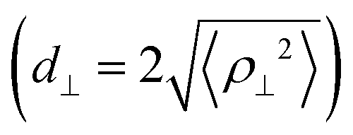 can be estimated as being ∼13 ± 2 nm and ∼5 ± 2 nm for the high- and low-energy excitons, respectively. This finding implies that the smaller nanodisks have a higher Bi composition, to account for the red shift of the emission.
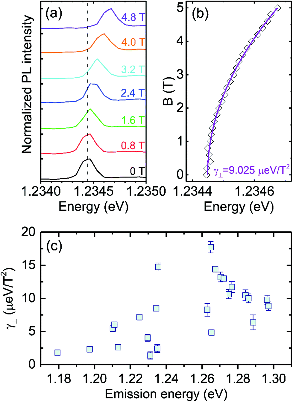 | ||
| Fig. 5 μ-PL spectra (a) of a representative PL line and its energy position (b) as a function of an applied magnetic field, B. The solid line in (b) is the best fit to the data (open diamonds) by using eqn (2) with γ⊥ = 9.025 μeV T−2. (c) Summary of the deduced diamagnetic coefficients (γ⊥) for emission lines with different energies. | ||
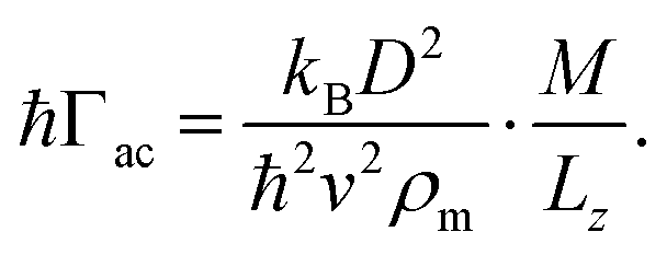
The interaction of excitons with acoustic phonons also corroborates this picture. Fig. 6(a) presents the temperature dependent linewidth of the PL lines at various emission energies. At low temperatures (T < 45 K), the emission linewidth is found to increase monotonically following a nearly linear temperature dependence. The strength of exciton coupling with optical phonons is expected to be negligible within this temperature range,54 considering the large LO phonon energy of ∼36 meV. Therefore, the linewidth broadening is predominantly caused by the exciton scattering with acoustic phonons via acoustic deformation potential, described by ħΓ(T) ≈ ħΓ0 + ħΓacT. Here ħΓ0 denotes the emission linewidth at 0 K and Γac is the exciton-acoustic phonon scattering rate. The slope ħΓac can be determined from the best fit to the experimental data, as shown by the solid lines in Fig. 6(a). We found that ħΓac increases from ∼2 μeV K−1 for the line at 1.2446 eV to ∼51.2 μeV K−1 for the low energy line at 1.1538 eV – see also Fig. 6(b). To understand this dependence, we note that in quantum well-like structures (e.g. nanodisks) the coupling strength between an exciton and acoustic phonon can be expressed by:54,61
 | (3) |
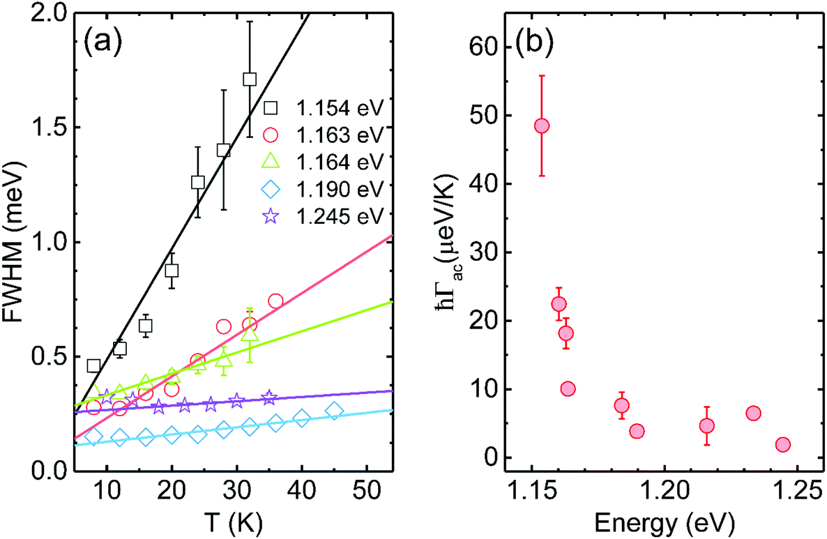 | ||
| Fig. 6 (a) Temperature dependence of FWHM for several emission lines. The solid lines are the best fits by eqn (3), allowing to extract the exciton–acoustic phonon scattering rate Γac. (b) The exciton–acoustic phonon coupling strength ħΓac as a function of the emission energy. | ||
Here, D, v, ρm are the inter-band hydrostatic deformation potential, longitudinal-acoustic phonon velocity and mass density, respectively. The in-plane exciton mass M is approximately a constant as discussed before. Lz is the effective disk thickness. Therefore, the increase of exciton-acoustic phonon coupling for the low-energy emission lines can be ascribed to enhanced lateral confinement, in agreement with the magneto-PL results. This suggests that Bi composition in thinner nanodisks is much higher than in the thicker ones.
In summary, we have investigated the formation of self-assembled nanodisks in GaAs/GaAsBi core–multishell NWs. Through detailed cross-sectional HRTEM and EDS characterization, we found that Bi favorably segregates within twin planes near the six 〈112〉 side corners, forming the nanodisks. Their formation is suggested to be strain driven and may also be affected by crystal polarity. The nanodisks induce exciton confinement, giving rise to a series of sharp emission lines with a linewidth below 450 μeV and energies ranging between 1.15 to 1.32 eV. Moreover, the observed increase of the exciton–acoustic phonon coupling for the low-energy emission lines deduced from the analysis of the temperature-dependent PL linewidth suggests that accumulation of Bi atoms is facilitated in thinner nanodisks. This conclusion is consistent with our magneto-PL data, which show that thin nanodisks are responsible for low-energy emissions and, therefore, have a higher Bi content. Our results, therefore, show that in addition to band structure engineering via bandgap bowing in GaAsBi alloys, the tendency of Bi to segregate within the spatial regions with well-defined crystallographic structure can be used for the fabrication of self-assembled quantum emitters embedded in GaAsBi NWs. This can be promising for future applications of this material system in advanced nanophotonic and quantum information devices based on single photon emitters.
Experimental details
The investigated GaAs/GaAsBi core–multishell nanowires were grown by Ga-catalyzed molecular beam epitaxy on phosphorus-doped n-type Si (111) substrates. The details of the growth process can be found elsewhere.19,20 To initiate the constituent Ga-induced vapor–liquid–solid growth, the inner GaAs core was grown for 15 min at 580 °C under As4 overpressure. During the growth, the As4 beam equivalent pressure was ∼1 × 10⁻⁵ mbar and the Ga beam flux was set to match the planar growth rate of 1.0 ML s−1 on a GaAs (001) substrate. Next, the growth was interrupted for 10 min to induce crystallization of the Ga catalyst on the tip of NWs. After the crystallization of the catalyst, lateral growth on the NWs sidewall became dominant, which enabled the formation of shell layers with precisely controlled thicknesses.19,20,62,63 Following the first growth interruption, the Ga flux was supplied for 15 min to finalize the formation of the 70 nm-wide GaAs core. The second growth interruption was introduced by reducing the substrate temperature to 350 °C, as required to achieve Bi incorporation. The beam equivalent pressure of Bi was adjusted to 5 × 10⁻⁷ mbar to obtain a GaAsBi shell with the targeted Bi concentration of 2%.19,20 The structure was then capped with the outer GaAs shell grown for 15 min at 350 °C. The NWs have ZB crystal structure as confirmed from HR-HAADF and electron diffraction measurements shown in Fig. 1 and 2, respectively.Morphological, structural and compositional analyses were performed by using SEM and cross-sectional STEM microscopies. STEM measurements were carried out on a TEM system (JEM-ARM200F Dual-X, JEOL) operating at 200 kV with EDS employing a 100 mm2 silicon drift detector (JED-2300, JEOL). STEM images were obtained in both bright-field BF and HAADF modes. Axially and radially sliced single NW samples were prepared by focused ion beam processing (Helios660, FEI). The details regarding the fabrication process for the radial and axial cross-sectional STEM investigations can be found in the ESI.† For optical characterization, nanowires were mechanically transferred onto gold-coated silica substrates, and then the samples were loaded into a variable-temperature cryostat equipped with a superconducting solenoid magnet (up to 5 T). All μ-PL measurements were performed on single NWs using a confocal Horiba Jobin–Yvon HR800 system, where the excitation light was produced by a solid-state 660 nm laser. The polarization-resolved PL signal was collected by a microscope objective (50×, NA = 0.5) in a backscattering geometry and analyzed with a rotatable half-wave plate together with a fixed linear polarizer.
Conflicts of interest
The authors declare no competing financial interest.Acknowledgements
The authors would like to acknowledge the financial support from the Swedish Research Council (Grant No. 2019-04312) and the Swedish Foundation for International Cooperation in Research and Higher Education (STINT) (Grant No. JA2014-5698). IB and WMC acknowledge financial support from the Swedish Government Strategic Research Area in Materials Science on Functional Materials at Linköping University (Faculty Grant SFO-Mat-LiU No. 2009 00971). The NW growth and structural characterization was supported by KAKENHI (Grants No. 19H00855 and 16H05970) from Japan Society of Promotion of Science.References
- H. J. Joyce, Q. Gao, H. Hoe Tan, C. Jagadish, Y. Kim, J. Zou, L. M. Smith, H. E. Jackson, J. M. Yarrison-Rice, P. Parkinson and M. B. Johnston, Prog. Quantum Electron., 2011, 35, 23–75 CrossRef
.
- J. Svensson, A. W. Dey, D. Jacobsson and L. E. Wernersson, Nano Lett., 2015, 15, 7898–7904 CrossRef CAS
- L. Hu and G. Chen, Nano Lett., 2007, 7, 3249–3252 CrossRef CAS
- S. Chen, M. Jansson, J. E. Stehr, Y. Huang, F. Ishikawa, W. M. Chen and I. A. Buyanova, Nano Lett., 2017, 17, 1775–1781 CrossRef CAS
- S. Chen, M. Yukimune, R. Fujiwara, F. Ishikawa, W. M. Chen and I. A. Buyanova, Nano Lett., 2019, 19, 885–890 CrossRef
- D. Saxena, S. Mokkapati, P. Parkinson, N. Jiang, Q. Gao, H. H. Tan and C. Jagadish, Nat. Photonics, 2013, 7, 963–968 CrossRef CAS
- B. Mayer, D. Rudolph, J. Schnell, S. Morkotter, J. Winnerl, J. Treu, K. Muller, G. Bracher, G. Abstreiter, G. Koblmuller and J. J. Finley, Nat. Commun., 2013, 4, 2931 CrossRef
- D. Saxena, N. Jiang, X. Yuan, S. Mokkapati, Y. Guo, H. H. Tan and C. Jagadish, Nano Lett., 2016, 16, 5080–5086 CrossRef CAS
- T. Burgess, D. Saxena, S. Mokkapati, Z. Li, C. R. Hall, J. A. Davis, Y. Wang, L. M. Smith, L. Fu, P. Caroff, H. H. Tan and C. Jagadish, Nat. Commun., 2016, 7, 11927 CrossRef CAS
- X. Dai, S. Zhang, Z. L. Wang, G. Adamo, H. Liu, Y. Z. Huang, C. Couteau and C. Soci, Nano Lett., 2014, 14, 2688–2693 CrossRef CAS
- M. Usman, Nanoscale, 2019, 11, 20133–20143 RSC
- B. Zhang, W. Y. Qiu, P. P. Chen and X. J. Wang, J. Appl. Phys., 2018, 123, 035702 CrossRef
- K. Alberi, J. Wu, W. Walukiewicz, K. M. Yu, O. D. Dubon, S. P. Watkins, C. X. Wang, X. Liu, Y. J. Cho and J. Furdyna, Phys. Rev. B: Condens. Matter Mater. Phys., 2007, 75, 045203 CrossRef
- K. Alberi, O. D. Dubon, W. Walukiewicz, K. M. Yu, K. Bertulis and A. Krotkus, Appl. Phys. Lett., 2007, 91, 051909 CrossRef
- S. J. Sweeney and S. R. Jin, J. Appl. Phys., 2013, 113, 043110 CrossRef
- M. Usman, C. A. Broderick, A. Lindsay and E. P. O'Reilly, Phys. Rev. B: Condens. Matter Mater. Phys., 2011, 84, 245202 CrossRef
- X. Wu, W. Pan, Z. Zhang, Y. Li, C. Cao, J. Liu, L. Zhang, Y. Song, H. Ou and S. Wang, ACS Photonics, 2017, 4, 1322–1326 CrossRef CAS
- I. P. Marko, C. A. Broderick, S. Jin, P. Ludewig, W. Stolz, K. Volz, J. M. Rorison, E. P. O'Reilly and S. J. Sweeney, Sci. Rep., 2016, 6, 28863 CrossRef CAS
- F. Ishikawa, Y. Akamatsu, K. Watanabe, F. Uesugi, S. Asahina, U. Jahn and S. Shimomura, Nano Lett., 2015, 15, 7265–7272 CrossRef CAS
- T. Matsuda, K. Takada, K. Yano, R. Tsutsumi, K. Yoshikawa, S. Shimomura, Y. Shimizu, K. Nagashima, T. Yanagida and F. Ishikawa, Nano Lett., 2019, 19, 8510–8518 CrossRef CAS
- M. Oliva, G. Gao, E. Luna, L. Geelhaar and R. B. Lewis, Nanotechnology, 2019, 30, 425601 CrossRef CAS
- B. Zhang, Y. Huang, J. E. Stehr, P. P. Chen, X. J. Wang, W. Lu, W. M. Chen and I. A. Buyanova, Nano Lett., 2019, 19, 6454–6460 CrossRef CAS
- B. Zhang, C. Chen, J. B. Han, C. Jin, J. X. Chen and X. J. Wang, AIP Adv., 2018, 8, 045021 CrossRef
- B. Zhang, M. Jansson, P. P. Chen, X. J. Wang, W. M. Chen and I. A. Buyanova, Nanotechnology, 2020, 31, 225706 CrossRef CAS
- B. Zhang, W. Y. Qiu, S. L. Chen, P. P. Chen, W. M. M. Chen, I. A. Buyanova and X. J. Wang, Appl. Phys. Lett., 2019, 114, 252101 CrossRef
- Y. Fontana, P. Corfdir, B. Van Hattem, E. Russo-Averchi, M. Heiss, S. Sonderegger, C. Magen, J. Arbiol, R. T. Phillips and A. F. I. Morral, Phys. Rev. B: Condens. Matter Mater. Phys., 2014, 90, 075307 CrossRef
- N. Jeon, D. Ruhstorfer, M. Doblinger, S. Matich, B. Loitsch, G. Koblmuller and L. Lauhon, Nano Lett., 2018, 18, 5179–5185 CrossRef CAS
- M. Heiss, Y. Fontana, A. Gustafsson, G. Wust, C. Magen, D. D. O'Regan, J. W. Luo, B. Ketterer, S. Conesa-Boj, A. V. Kuhlmann, J. Houel, E. Russo-Averchi, J. R. Morante, M. Cantoni, N. Marzari, J. Arbiol, A. Zunger, R. J. Warburton and A. F. I. Morral, Nat. Mater., 2013, 12, 439–444 CrossRef CAS
- C. Zheng, J. Wong-Leung, Q. Gao, H. H. Tan, C. Jagadish and J. Etheridge, Nano Lett., 2013, 13, 3742–3748 CrossRef CAS
- T. Shi, H. E. Jackson, L. M. Smith, N. Jiang, Q. Gao, H. H. Tan, C. Jagadish, C. Zheng and J. Etheridge, Nano Lett., 2015, 15, 1876–1882 CrossRef CAS
- N. Skold, J. B. Wagner, G. Karlsson, T. Hernan, W. Seifert, M. E. Pistol and L. Samuelson, Nano Lett., 2006, 6, 2743–2747 CrossRef
- H. A. Fonseka, A. V. Velichko, Y. Zhang, J. A. Gott, G. D. Davis, R. Beanland, H. Liu, D. J. Mowbray and A. M. Sanchez, Nano Lett., 2019, 19, 4158–4165 CrossRef CAS
- Y. Zhang, A. M. Sanchez, J. Wu, M. Aagesen, J. V. Holm, R. Beanland, T. Ward and H. Liu, Nano Lett., 2015, 15, 3128–3133 CrossRef CAS
- L. Francaviglia, G. Tutuncuoglu, S. Marti-Sanchez, E. Di Russo, S. E. Steinval, J. S. Ruiz, H. Potts, M. Friedl, L. Rigutti, J. Arbiol and A. F. I. Morral, Phys. Rev. Mater., 2019, 3, 023001 CrossRef CAS
- J. Claudon, J. Bleuse, N. S. Malik, M. Bazin, P. Jaffrennou, N. Gregersen, C. Sauvan, P. Lalanne and J. M. Gerard, Nat. Photonics, 2010, 4, 174–177 CrossRef CAS
- G. Bulgarini, M. E. Reimer, M. Hocevar, E. P. A. M. Bakkers, L. P. Kouwenhoven and V. Zwiller, Nat. Photonics, 2012, 6, 455–458 CrossRef CAS
- S. Filippov, M. Jansson, J. E. Stehr, J. Palisaitis, P. O. Persson, F. Ishikawa, W. M. Chen and I. A. Buyanova, Nanoscale, 2016, 8, 15939–15947 RSC
- M. Jansson, F. Ishikawa, W. M. Chen and I. A. Buyanova, Phys. Rev. Appl., 2018, 10, 044040 CrossRef CAS
- M. Jansson, L. Francaviglia, R. La, C. W. Tu, W. M. Chen and I. A. Buyanova, Phys. Rev. Mater., 2020, 4, 056005 CrossRef CAS
- T. Burgess, S. Breuer, P. Caroff, J. Wong-Leung, Q. Gao, H. Hoe Tan and C. Jagadish, ACS Nano, 2013, 7, 8105–8114 CrossRef CAS
- N. Isik Goktas, A. Sokolovskii, V. G. Dubrovskii and R. R. LaPierre, Nano Lett., 2020, 20, 3344–3351 CrossRef CAS
- D. T. J. Hurle and P. Rudolph, J. Cryst. Growth, 2004, 264, 550–564 CrossRef CAS
-
W. Shu, X. Zhang, X. Liu, H. Huang, Y. Huang and X. Ren, Advances in Optoelectronics and Micro/nano-optics, 2010, pp. 1–3, DOI:10.1109/AOM.2010.5713533
- K. Jacobi, J. Platen, C. Setzer, J. Marquez, L. Geelhaar, C. Meyne, W. Richter, A. Kley, P. Ruggerone and M. Scheffler, Surf. Sci., 1999, 439, 59–72 CrossRef CAS
- A. Jenichen and C. Engler, Surf. Sci., 2013, 608, 204–211 CrossRef CAS
- M. Wu, E. Luna, J. Puustinen, M. Guina and A. Trampert, Nanotechnology, 2014, 25, 205605 CrossRef
- D. N. Macfadyen, J. Electrochem. Soc., 1983, 130, 1934–1941 CrossRef CAS
- S. Iida and K. Ito, J. Electrochem. Soc., 1971, 118, 768 CrossRef
- B. Yang, F. Liu and M. G. Lagally, Phys. Rev. Lett., 2004, 92, 025502 CrossRef
- R. B. Lewis, L. Nicolai, H. Kupers, M. Ramsteiner, A. Trampert and L. Geelhaar, Nano Lett., 2017, 17, 136–142 CrossRef CAS
- Y. N. Guo, T. Burgess, Q. Gao, H. H. Tan, C. Jagadish and J. Zou, Nano Lett., 2013, 13, 5085–5089 CrossRef CAS
- W. Choi, E. Seabron, P. K. Mohseni, J. D. Kim, T. Gokus, A. Cernescu, P. Pochet, H. T. Johnson, W. L. Wilson and X. Li, ACS Nano, 2017, 11, 1530–1539 CrossRef CAS
- W. Chen, L. Yu, S. Misra, Z. Fan, P. Pareige, G. Patriarche, S. Bouchoule and P. Roca i Cabarrocas, Nat. Commun., 2014, 5, 4134 CrossRef CAS
- A. M. Graham, P. Corfdir, M. Heiss, S. Conesa-Boj, E. Uccelli, A. Fontcuberta i Morral and R. T. Phillips, Phys. Rev. B: Condens. Matter Mater. Phys., 2013, 87, 125304 CrossRef
- P. Corfdir, B. Van Hattem, E. Uccelli, A. F. I. Morral and R. T. Phillips, Appl. Phys. Lett., 2013, 103, 133109 CrossRef
- D. Spirkoska, J. Arbiol, A. Gustafsson, S. Conesa-Boj, F. Glas, I. Zardo, M. Heigoldt, M. H. Gass, A. L. Bleloch, S. Estrade, M. Kaniber, J. Rossler, F. Peiro, J. R. Morante, G. Abstreiter, L. Samuelson and A. F. I. Morral, Phys. Rev. B: Condens. Matter Mater. Phys., 2009, 80, 245325 CrossRef
- P. Corfdir, H. Kupers, R. B. Lewis, T. Flissikowski, H. T. Grahn, L. Geelhaar and O. Brandt, Phys. Rev. B, 2016, 94, 155413 CrossRef
- G. Moody, R. Singh, H. Li, I. A. Akimov, M. Bayer, D. Reuter, A. D. Wieck, A. S. Bracker, D. Gammon and S. T. Cundiff, Phys. Rev. B: Condens. Matter Mater. Phys., 2013, 87, 041304 CrossRef
- S. N. Walck and T. L. Reinecke, Phys. Rev. B: Condens. Matter Mater. Phys., 1998, 57, 9088–9096 CrossRef CAS
- G. Pettinari, A. Polimeni, J. H. Blokland, R. Trotta, P. C. M. Christianen, M. Capizzi, J. C. Maan, X. Lu, E. C. Young and T. Tiedje, Phys. Rev. B: Condens. Matter Mater. Phys., 2010, 81, 235211 CrossRef
- P. Borri, W. Langbein, J. M. Hvam and F. Martelli, Phys. Rev. B: Condens. Matter Mater. Phys., 1999, 59, 2215–2222 CrossRef CAS
- Y. Araki, M. Yamaguchi and F. Ishikawa, Nanotechnology, 2013, 24, 065601 CrossRef
- N. Ahn, Y. Araki, M. Kondow, M. Yamaguchi and F. Ishikawa, Jpn. J. Appl. Phys., 2014, 53, 065001 CrossRef
Footnote |
| † Electronic supplementary information (ESI) available: Fabrication process of the samples for radial and axial cross-sectional STEM investigations, and a series of STEM images. See DOI: 10.1039/d0nr05488g |
| This journal is © The Royal Society of Chemistry 2020 |