
 Open Access Article
 This Open Access Article is licensed under a Creative Commons Attribution-Non Commercial 3.0 Unported Licence
Nanoscale phenomena ruling deposition and intercalation of AlN at the graphene/SiC interface†
Anelia
Kakanakova-Georgieva
 *a,
Gueorgui K.
Gueorguiev
a,
Davide G.
Sangiovanni
a,
Nattamon
Suwannaharn
ab,
Ivan G.
Ivanov
a,
Ildikó
Cora
c,
Béla
Pécz
c,
Giuseppe
Nicotra
d and
Filippo
Giannazzo
d
*a,
Gueorgui K.
Gueorguiev
a,
Davide G.
Sangiovanni
a,
Nattamon
Suwannaharn
ab,
Ivan G.
Ivanov
a,
Ildikó
Cora
c,
Béla
Pécz
c,
Giuseppe
Nicotra
d and
Filippo
Giannazzo
d
aDepartment of Physics, Chemistry and Biology (IFM), Linköping University, 581 83 Linköping, Sweden. E-mail: anelia.kakanakova@liu.se
bNanoscience and Technology Program, Graduate School, Chulalongkorn University, Bangkok, 10330, Thailand
cCentre for Energy Research, Institute of Technical Physics and Materials Science, Konkoly-Thege M. út 29-33, Budapest, 1121, Hungary
dConsiglio Nazionale delle Ricerche, Istituto per la Microelettronica e Microsistemi, Strada VIII, n. 5, Zona Industriale, I-95121, Catania, Italy
First published on 17th September 2020
Abstract
The possibility for kinetic stabilization of prospective 2D AlN was explored by rationalizing metal organic chemical vapor deposition (MOCVD) processes of AlN on epitaxial graphene. From the wide range of temperatures which can be covered in the same MOCVD reactor, the deposition was performed at the selected temperatures of 700, 900, and 1240 °C. The characterization of the structures by atomic force microscopy, electron microscopy and Raman spectroscopy revealed a broad range of surface nucleation and intercalation phenomena. These phenomena included the abundant formation of nucleation sites on graphene, the fragmentation of the graphene layers which accelerated with the deposition temperature, the delivery of excess precursor-derived carbon adatoms to the surface, as well as intercalation of sub-layers of aluminum atoms at the graphene/SiC interface. The conceptual understanding of these nanoscale phenomena was supported by our previous comprehensive ab initio molecular dynamics (AIMD) simulations of the surface reaction of trimethylaluminum, (CH3)3Al, precursor with graphene. A case of applying trimethylindium, (CH3)3In, precursor to epitaxial graphene was considered in a comparative way.
Introduction
Aluminum nitride (AlN) is a prototype material which can undergo relaxation from a 2D “graphitic-like” structure with planar trigonal sp2 bond coordination (h-AlN) to its common 3D wurtzite structure with tetrahedral sp3 bond coordination (wz-AlN).1 In general, the stability of the “graphitic-like” structure with respect to the wurtzite structure has been predicted to be dependent on the number of monolayers. This maximum number of monolayers has been calculated to be as many as about twenty in the case of 2D AlN; and to be far exceeding the maximum number of monolayers calculated for other materials including 2D GaN, 2D ZnO, and 2D BeO.1 2D AlN has motivated a wide-reaching interest in connection with nanoscale optoelectronics and room-temperature spintronics, and has been extensively studied via first principles calculations.2–8 Structural optimization of its free-standing monolayer and few-layer conformations, stability analysis, electronic structure, and optical properties have been presented.2–8 Initial theoretical results have been corroborated by experimental evidence for “graphitic-like” AlN represented by 12 sp2-bonded monolayers obtained under scanning tunneling microscopy conditions on catalytic substrates of Ag (111).9 Subsequently, formation of “graphitic-like” AlN has also been achieved under molecular beam epitaxy conditions on substrates of Si (111).10 In the latter experiments, onset of “graphitic-like” to wurtzite structural relaxation has been observed for 5–6 monolayers of h-AlN. The effect has been attributed to a bulk stabilization mechanism via structural defects and roughening.10Thus far, the realization of 2D AlN has been demonstrated under stringent ultra-high vacuum conditions and on specific substrates, which admittedly aims at a well-balanced deposition kinetics. By the account of a recently published article, an effort has been put in obtaining 2D AlN by metal organic chemical vapor deposition (MOCVD).11 The all-important control over the deposition kinetics, in order to stabilize the ultrathin structure of 2D AlN, has been achieved by adopting the concept of 2D material intercalation in a confined space. In that study,11 a confined space has been created by transferring graphene on a substrate of Si (111). The concept of 2D material intercalation has originally been applied to stabilize 2D GaN at the interface between quasi-free-standing epitaxial graphene (QFSEG) and a hydrogen passivated SiC substrate surface.12
Any rational deposition of 2D materials, including the herein referred 2D GaN and 2D AlN, motivates the use of MOCVD for being the scalable and industrially compatible deposition process of relevance to well-established and emerging 2D semiconductors and heterostructures.
To date, MOCVD conditions of annealing of epitaxial graphene in a flow of molecular hydrogen have regularly been applied in order to decouple the notorious carbon buffer layer from the SiC substrate, form a monolayer of QFSEG atop, and tune the properties of graphene for perceived electronic applications.13 Importantly, the hydrogen intercalation also accomplishes a regular termination of the Si dangling bonds, which opens the possibility for 2D materials to be deposited on SiC substrates. The possibility for 2D materials to be deposited on 3D substrates has previously been demonstrated under the conditions of molecular beam epitaxy of naturally layered transition metal dichalcogenides on sulfur-terminated substrates of GaAs (111) and GaSe on hydrogen-terminated substrates of Si (111).14
Despite being a major research subject with a large availability of experimental data, key atomic-scale mechanisms which control hydrogen intercalation of epitaxial graphene under MOCVD conditions are yet to be fully understood.15 This is particularly the case for the dissociative chemisorption and diffusion of hydrogen on graphene. In this regard, ab initio molecular dynamics (AIMD) simulations are an indispensable tool of investigation. However, to our knowledge, AIMD simulations have not been employed for the investigation of hydrogen intercalation phenomena. Advantageous to the conceptual understanding of dissociative chemisorption and intercalation phenomena under MOCVD conditions in general, our recent AIMD study reveals atomistic and electronic processes responsible for delivery of aluminum (Al) adatoms on pristine graphene consequent to surface reactions of trimethylaluminum, (CH3)3Al, precursor with graphene.16 The achieved understanding of the complex precursor/surface dynamics and reaction mechanisms at atomistic level enables more efficient exploitation of the chemical precursors and better control of the MOCVD processes for the formation of 2D materials.16 It is noticeable that currently available experimental data on intercalation phenomena under MOCVD conditions, which apply common metal organic precursors such as (CH3)3Al and (CH3)3Ga, is limited to the only two demonstrations of 2D AlN11 and 2D GaN.12
The present study corroborates MOCVD of AlN on epitaxial graphene with surface and interface characterization and establishes a link to our previous comprehensive AIMD simulations of the (CH3)3Al/graphene surface reactions.16 The research outcome masters the understanding of dissociative chemisorption, nucleation and intercalation phenomena ruling the MOCVD of AlN on epitaxial graphene. Forming AlN at nanoscale is explicitly conditioned by the specificity of the reaction pathways of dissociative chemisorption of the (CH3)3Al precursor on graphene at atomistic level. To emphasize this understanding, a case of comparison of applying trimethylindium, (CH3)3In, precursor to epitaxial graphene is also divulged.
Experimental
The MOCVD processes were performed in a horizontal-type hot-wall MOCVD reactor (GR508GFR AIXTRON) which is implemented for the research and development of group III nitrides of semiconductor quality.17 The epitaxial graphene on 4H-SiC (0001), which represented the substrate used, was fabricated by high-temperature sublimation technique,18 whereby the buffer layer can successfully be decoupled from the SiC by hydrogen intercalation under the MOCVD conditions in the reactor.19,20 Typical size of the samples of epitaxial graphene was 7 × 7 mm2. The epitaxial graphene was heated in the gas-flow of H2 up to the temperature of 700, 900 or 1240 °C. The gas-flow rate of H2 was at 25 slm. The reactor was operated at a pressure of 200 mbar. Trimethylaluminum, (CH3)3Al, and ammonia, NH3, were employed as precursors at the gas-flow rate of 0.7 sccm and 2.0 slm, respectively. The scheme of precursor delivery involved 3 cycles in total, each of about 3 minutes and consisting of alternating (CH3)3Al with NH3 followed by an extra time of 10 minutes of joint delivery of the precursors (CH3)3Al and NH3. The flow of NH3 and H2 continued during the cooling down stage of the overall MOCVD process.The morphology of the samples was evaluated by tapping mode atomic force microscopy (AFM) using Si probes and a DI3100 equipment with a Nanoscope V controller.
Transparent TEM specimens were thinned by both conventional Ar ion milling using Technoorg Linda millers and by FIB (Focused Ion Beam) technique using a FEI SCIOS2 unit in which the energy of Ga ions was reduced to 2 keV. To keep the top region of the sample intact, an aluminum layer was evaporated with a thin amorphous carbon at the bottom. TEM lamella were studied by transmission electron microscopy (TEM) using a JEOL3010 (LaB6, 300 keV) and a JEOL ARM 200F (200 keV probe corrected) microscopes.
STEM analyses were performed on the probe corrected JEOL ARM 200F at 200 keV of primary beam energy with a beam convergence half-angle of 33 mrad for an estimated probe size of 0.68 Å. In the high angle annular dark field (HAADF) configuration, inner and outer radii were set at 90 and 190 mrad, respectively. For the annular bright field (ABF) inner and outer radii were set at 11 and 24 mrad, respectively.
The Raman spectra were registered using a home-built micro-Raman setup based on a monochromator (Jobin–Yvon, model HR460) equipped with a charge-coupled device (CCD) camera. The objective lens has a magnification of 100× and numerical aperture NA = 0.95 resulting in a ∼0.85 μm diameter of the laser spot focused on the sample surface. A 532 nm solid-state laser was used as an excitation source. The power was kept below 1 mW to avoid thermal damage of the sample. The spectral resolution of the system is ∼5.5 cm−1.
Results and discussion
This study develops from a set of samples representing MOCVD of AlN on epitaxial graphene whereby the MOCVD conditions were defined by the applied temperature: 700, 900, and 1240 °C. The temperature of 700 °C has been used for the achievement of intercalated layers of indium (In) atoms in the same reactor, as shown further below, using the same deposition protocol. The temperature of 900 °C has been used for the accomplishment of hydrogen intercalation of epitaxial graphene which is evidenced by the appearance of a characteristic Raman phonon peak ascribed to the formation of Si–H bonds.20 Investigation on the annealing of the epitaxial graphene in molecular hydrogen only and without the (CH3)3Al precursor, and in the same reactor, is therefore available through our previous study published under ref. 20. The high temperature of 1240 °C is typically used for the deposition of wz-AlN of semiconductor quality on either SiC or AlN substrates in the same MOCVD reactor.17 An early study about the impact of epitaxial graphene on AlN nucleation at reduced temperatures can be followed in ref. 21 being part of the ongoing debate about MOCVD of AlN and GaN on graphene.Fig. 1 reports the AFM morphologies along with representative height line-scans for the AlN deposited at the temperature of 700 °C (a), 900 °C (b) and 1240 °C (c). It can be observed how the MOCVD of AlN at 700 °C and 900 °C is associated with the development of rough nanostructured films, while spreading of flat coalesced areas characterizes the deposition of AlN at the high temperature of 1240 °C. An evolution of the film nanostructure can also be noticed with the increase of the deposition temperature from 700 to 900 °C. While a disordered nanograin structure is found at the lower temperature, the formation of larger AlN grains with overlapped small needles structures is observed at 900 °C. For the AlN deposited at 1240 °C, extended and flat coalesced areas with thickness in the order of 100 nm can be deduced from the morphology and line-scan in Fig. 1(c). This initial observation by AFM on the evolution of the AlN morphology is consistent with the expected effect of the high deposition temperature on the improvement of the material quality of AlN deposited on either SiC or AlN substrates.17
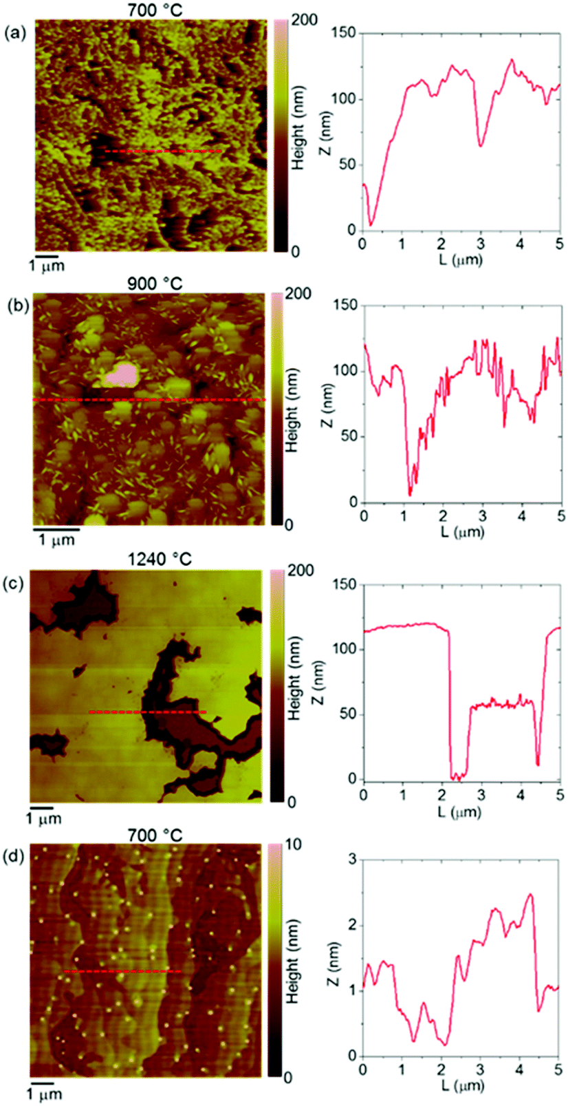 | ||
| Fig. 1 Atomic force microscopy (AFM) images and height line-scans for AlN deposited on epitaxial graphene at 700 °C (a), 900 °C (b), and 1240 °C (c). (d) AFM image and height line-scan for epitaxial graphene subjected to MOCVD at 700 °C with the (CH3)3In precursor. Shown for the purpose of comparison to (a). Note the different height scale. | ||
The results of our experiments imply that there is a remarkable density of nucleation sites on the graphene surface which contributes the development of the AlN nanostructured films. The functionalization of the graphene is directly linked to the dissociative adsorption of the (CH3)3Al precursor, consequent to the (CH3)3Al/graphene surface reactions, as revealed by our AIMD simulations.16 The (CH3)3Al/graphene surface reactions predominantly evolve via CH3-Al![[double bond, length as m-dash]](https://www.rsc.org/images/entities/char_e001.gif) C·H2 radical dissociation on graphene after the initial elimination of a methane molecule. Independent AIMD simulation runs consistently identify reaction pathways which lead to the delivery of aluminum (Al) adatoms as well as carbon (C) adatoms to the graphene consequent to the (CH3)3Al/graphene surface reactions. The high residence time of the Al adatoms on graphene (Al adatom desorption never observed despite the elevated temperature used in the AIMD simulations) is indicative of relatively strong Al binding to graphene. In addition, the migration rates of the Al adatoms on graphene increase dramatically (two-regime Arrhenius trends with upward bending of ln(rate) vs. 1/T) for temperatures exceeding 900 °C, as revealed by our AIMD modeling.16 The rapid enhancement in adatom diffusivity with temperature may further promote nucleation of AlN, with the Al adatom itself acting as initial seed.
C·H2 radical dissociation on graphene after the initial elimination of a methane molecule. Independent AIMD simulation runs consistently identify reaction pathways which lead to the delivery of aluminum (Al) adatoms as well as carbon (C) adatoms to the graphene consequent to the (CH3)3Al/graphene surface reactions. The high residence time of the Al adatoms on graphene (Al adatom desorption never observed despite the elevated temperature used in the AIMD simulations) is indicative of relatively strong Al binding to graphene. In addition, the migration rates of the Al adatoms on graphene increase dramatically (two-regime Arrhenius trends with upward bending of ln(rate) vs. 1/T) for temperatures exceeding 900 °C, as revealed by our AIMD modeling.16 The rapid enhancement in adatom diffusivity with temperature may further promote nucleation of AlN, with the Al adatom itself acting as initial seed.
Carbon adatoms form via dehydrogenation of CH2 admolecules on graphene.16 The delivery of carbon adatoms to the graphene induces partial reorganization of the graphene electron distribution in the vicinity of the adsorption site. This effect is expected to: (i) increase the local reactivity of pristine graphene, which may promote condensation of larger admolecules, or, in presence of surface imperfections, such as voids, (ii) further contribute to weakening C–C bonds in the graphene layer, which may induce local transformations of the bonding network, enlargement of defects and breakage of the graphene layers.
Atomic-scale mechanisms analogous to those mentioned above may be responsible for the gradual fragmentation of graphene as observed in the high resolution TEM images in Fig. 2(a–c). Temperatures higher than 700 °C apparently facilitate the (CH3)3Al/graphene surface reactions, thus accelerating decomposition of the graphene layers. After deposition of AlN at 900 °C, fragments of 2–3 layers of graphene could be identified, whereby individual graphene layers display discontinuity, Fig. 2(b). The graphene layers are displaced from the SiC substrate at about 4.2 ± 0.2 Å, and the distance between the graphene layers is the same. It might be noted that the first continuous graphene layer is seen in the double distance from the SiC substrate. Finally, after deposition of AlN at 1240 °C, graphene could not be located at the AlN/SiC interface, Fig. 2(c). In accordance with the initial AFM measurements, the applied temperature of 1240 °C results in the formation of about 150 nm thick film of AlN. It may spread over the SiC substrate as crystallites of up to 4 micrometer long. A low magnification TEM image of an AlN crystallite and further notes on TEM of the studied samples are included in the ESI.†
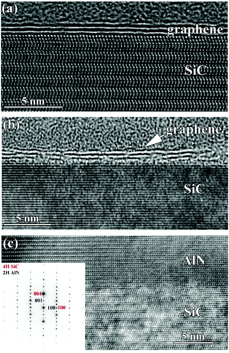 | ||
| Fig. 2 High resolution TEM image representative of graphene/SiC interface after deposition of AlN on epitaxial graphene at 700 °C (a) and 900 °C (b), and AlN/SiC interface after deposition at 1240 °C (c). The inset shows selected area electron diffraction (SAED) pattern of AlN which indicates epitaxial relationship to the SiC substrate. | ||
The comprehension of the structural characteristics of the samples is corroborated by the appearance of the related Raman spectra. Fig. 3 compares the Raman spectra (without subtraction of the SiC substrate spectrum) following the MOCVD with the (CH3)3Al precursor at the deposition temperature of 700 °C (a), 900 °C (b), and 1240 °C (c). The Raman spectrum of the sample deposited at 700 °C clearly displays the 2D peak of graphene, Fig. 3(a), being of characteristic full width at half maximum of about 30 cm−1. However, the dominating feature is a broad spectrum of two intense bands, resembling the D and G bands of amorphous carbon.22 Another broad band appears underneath the 2D peak of graphene. Thus, these bands are overlapping the characteristic peaks of graphene, Fig. 3(a). These bands might be arising from excess carbon species introduced to the surface because of the dissociative adsorption of the (CH3)3Al precursor, consequent to the (CH3)3Al/graphene surface reactions, as discussed above.
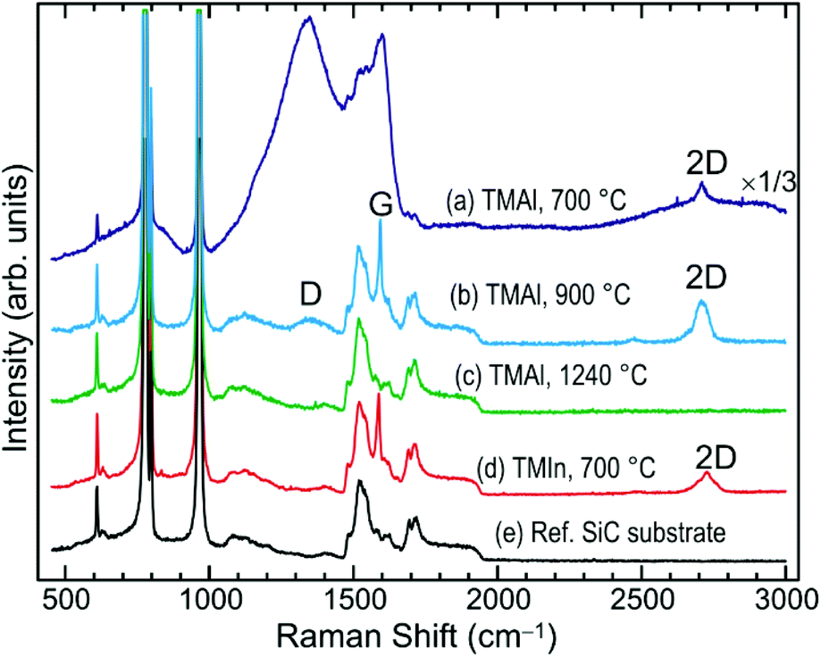 | ||
| Fig. 3 Raman spectra following the MOCVD with the (CH3)3Al precursor (TMAl) at a deposition temperature of 700 °C (a), 900 °C (b), and 1240 °C (c). (d) Raman spectrum following MOCVD with the (CH3)3In precursor (TMIn) at a deposition temperature of 700 °C. Shown for the purpose of comparison to the spectrum in (a). (e) Reference Raman spectrum of 4H-SiC showing the first and second order Raman contributions of the substrate spectrum in the rest of the spectra. Note the scale change in the top curve. | ||
Accumulation of amorphous carbon due to the dissociative adsorption of the (CH3)3Al precursor is also expected for the sample deposited at 900 °C. In fact, its contribution to the Raman spectra has been observed, but only after some annealing which occurs naturally in the laser spot during the Raman measurement despite the low laser power of <1 mW. Details of these measurements together with the related figure are included in the ESI.†
The G peak in the Raman spectrum of the sample deposited at 900 °C is overlaid by the second-order Raman bands of the SiC substrate, Fig. 3(b). The G mode in graphene is related to the bond stretching of all pairs of sp2 carbon atoms.22 Thus, the G peak appears in the Raman spectrum of the sample deposited at 900 °C although the graphene layers have apparently sustained damage in atomic order and continuity, Fig. 2(b). This is reflected in the appearance of a D band in its spectrum, Fig. 3(b). The 2D peak in this spectrum exhibits structure typical for bilayer graphene, which is in line with the TEM results presented above in Fig. 2(b). On the other hand, the G and 2D peak are indiscernible in the Raman spectrum of the sample deposited at 1240 °C, Fig. 3(c), which agrees with the lack of graphene at the AlN/SiC interface, Fig. 2(c).
The characteristic E2 (high) phonon mode of 2D AlN is expected at 659.9 cm−1. However, its direct observation in the Raman spectra using the 532 nm laser excitation is deemed very difficult for reasons as explained in detail in the ESI.†
It is worth stressing that the formation of Al and C adatoms on the graphene is a direct consequence of the dissociative adsorption of the (CH3)3Al precursor itself.16 It can rationalize the abundance of nucleation sites and the development of the AlN nanostructured film, Fig. 1(a). The increased reactivity of graphene in the vicinity of adsorbed species, unsaturated bonds at surface imperfections and breakages in the graphene network can provide not only for nucleation sites but also for penetration sites for atom intercalation. For example, regions of intercalated GaN have typically been found near 3D islands of GaN on the graphene surface.12
This brought about expectation of locating intercalated Al atoms at the graphene/SiC interface. By comparison, intercalated layers of indium (In) atoms using the same deposition protocol in the same reactor can be achieved. Fig. 4 (on the left) shows a high angle annular dark field scanning TEM (HAADF-STEM) image of the graphene/SiC interface after the MOCVD at 700 °C with the (CH3)3Al precursor. Fig. 4 (on the right) shows HAADF-STEM image of the graphene/SiC interface after the MOCVD at 700 °C with the (CH3)3In precursor. An intercalated structure with two sub-layers of In atoms can clearly be seen at the graphene/SiC interface. Since the contrast of the HAADF images is highly dependent on the atomic number, this ensures the discernibility between the intercalated Al and In atoms at the graphene/SiC interface in a comparative way (Fig. 4). Details of the applied TEM based chemical analyses (EDS and EELS) to the intercalated structure with sub-layers of Al are included in the ESI.†
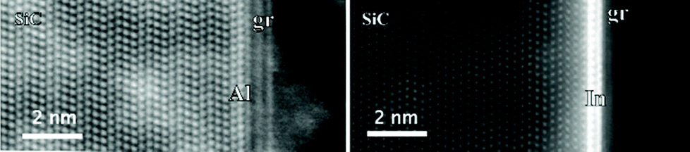 | ||
| Fig. 4 HAADF-STEM images of the graphene/SiC interface after MOCVD at 700 °C with the (CH3)3Al precursor (left), and (CH3)3In precursor (right). The sub-layers of intercalated Al and In atoms are correspondingly labeled. | ||
The graphene/SiC interface after the MOCVD at 700 °C with the (CH3)3Al precursor was investigated in more detail, Fig. 5 (top image). Since the HAADF-STEM provides direct atomic-resolution information about the specimen, we used this image to precisely evaluate the interlayer distance of the different atomic planes. The measurement was easily done on the plotted intensity line scan, represented by the redline on the superimposed magnified image, by measuring the distance between the centers of the peaks.
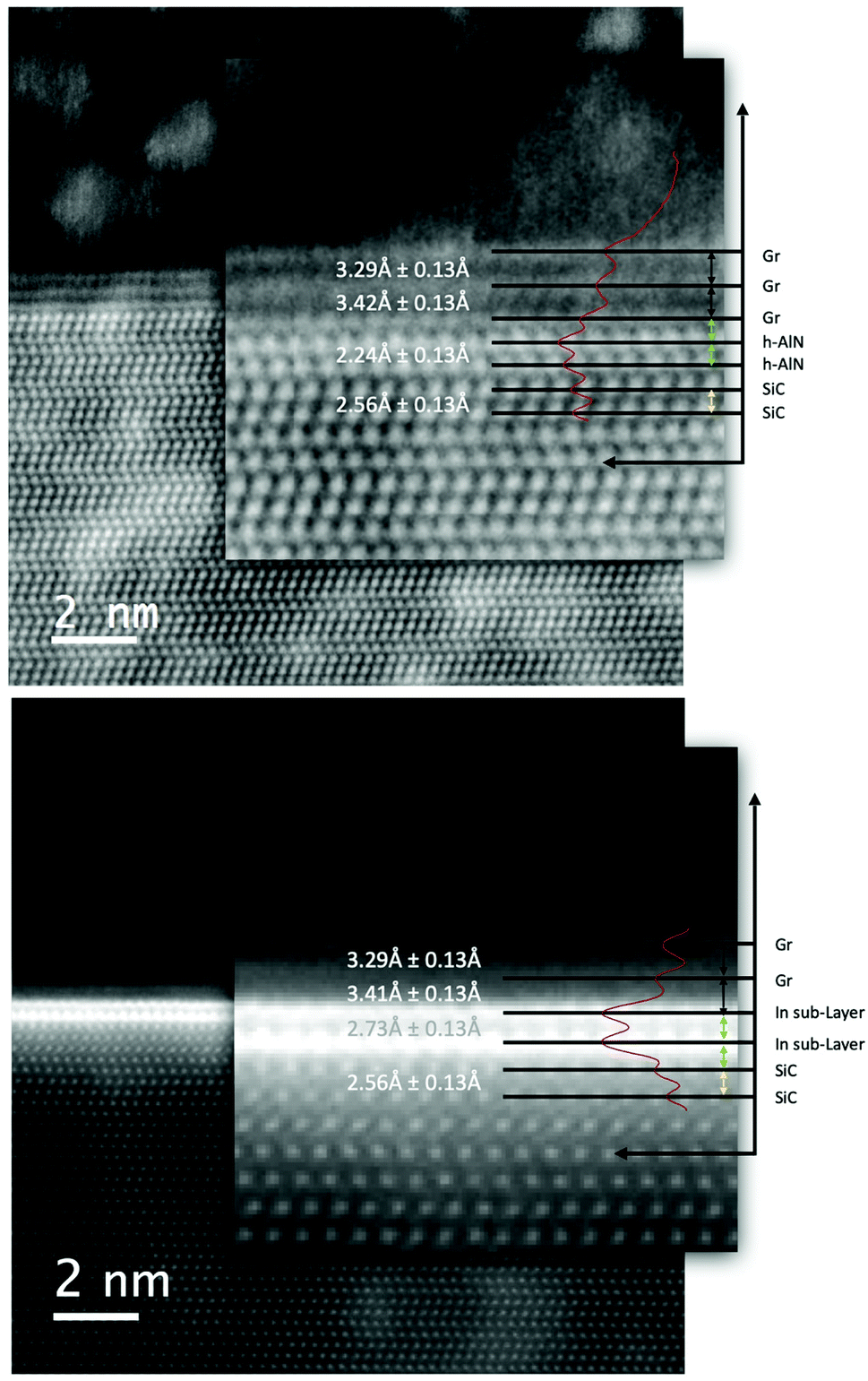 | ||
| Fig. 5 HAADF-STEM images of the intercalated structures with sub-layers of Al (top) and In atoms (bottom), same as in the Fig. 4. The intensity profile, represented by the red line on the magnified image, was used to precisely measure the interlayer distances as reported. Any intercalated Al atoms may supply the formation of “graphitic-like” h-AlN (see main text). | ||
While the characteristic distances between the different graphene layers, as well as the planar (0001) SiC surfaces have been confirmed, we observe two layers located at the graphene/SiC interface that exhibit markedly different, smaller interlayer distance of 2.24 Å. It could be speculated that any intercalated Al atoms may supply the formation of “graphitic-like” AlN. This speculation is substantiated with the calculated characteristic interlayer distances for few-layer free-standing h-AlN by density functional theory (DFT). The interlayer distance in bilayer h-AlN has been reported as 2.13 Å and thus being much smaller than the interlayer distance in bilayer h-BN or graphene, and indicative of a strong interlayer interaction.6 Moreover, for the relaxed structures of stacks of bilayer h-AlN with graphene, as calculated within the framework of DFT, the interlayer distance in bilayer h-AlN has been reported as 2.20 Å,7 giving a close comparison to the interlayer distance measured from the top image in Fig. 5. By comparison, the two sub-layers of intercalated In atoms exhibit a larger interlayer distance of 2.73 Å, Fig. 5 (bottom image).
The case of applying the (CH3)3In precursor to the epitaxial graphene, instead of the (CH3)3Al precursor, presents certain differences when comparing the associated surface morphology and Raman spectra. A very different surface morphology, displaying flat terraces separated by sub-nanometer high steps, can be observed after the MOCVD at 700 °C with the (CH3)3In precursor, Fig. 1(d). Unlike the case of applying the (CH3)3Al precursor, Fig. 1(a), with the (CH3)3In precursor apparently there is a reduced spreading of nuclei on the surface of the graphene. Also, there is no recurrence of the intense and broad amorphous-carbon-resembling spectrum, which is a very distinguishable feature of the Raman spectrum of the epitaxial graphene following its functionalization by the (CH3)3Al precursor (spectrum (d) vs. spectrum (a) in Fig. 3). This comparative presentation has been focused on how deposition at nanoscale could explicitly result from different reaction pathways of dissociative adsorption of the two precursors, (CH3)3Al and (CH3)3In, on graphene at atomistic level.
Conclusions
The possibility for kinetic stabilization of prospective 2D AlN was explored by rationalizing MOCVD processes of AlN on epitaxial graphene. From the wide range of temperatures which can be covered in the same MOCVD reactor, the deposition was performed at the selected temperatures of 700, 900, and 1240 °C. The reduced temperatures of 700 and 900 °C have previously been established to enable deposition control at the nanoscale for the achievement of intercalated layers of indium atoms, as well as hydrogen intercalation of epitaxial graphene, respectively. The high temperature of 1240 °C has previously been established for the deposition of semiconductor quality AlN on SiC substrates in the same reactor. A broad range of surface, nucleation and intercalation phenomena was revealed by the characterization of the structures by AFM, (S)TEM, and Raman spectroscopy. These phenomena included the abundant formation of nucleation sites on graphene, the fragmentation of the graphene layers which accelerated with the deposition temperature, the accumulation of amorphous carbon from the excess precursor-derived C adatoms, as well as intercalation of Al atoms at the graphene/SiC interface, which may supply the formation of “graphitic-like” AlN. The conceptual understanding of these nanoscale phenomena, as evidenced from the characterization of the structures, was supported by our previous comprehensive AIMD simulations of the (CH3)3Al/graphene surface reactions. A case of comparison by applying the (CH3)3In precursor to epitaxial graphene was also divulged to emphasize the understanding that forming AlN at nanoscale is explicitly conditioned by the specificity of the reaction pathways of dissociative chemisorption of the (CH3)3Al precursor on graphene at atomistic level.Conflicts of interest
There are no conflicts to declare.Acknowledgements
The authors thank Dr T. Iakimov and Prof. R. Yakimova for kindly providing samples of epitaxial graphene. The authors thank N. Szász and L. Illés for sample preparation. This work was supported by FLAG-ERA 2015 JTC project GRIFONE through Swedish Research Council VR 2015-06816 (A. Kakanakova, project leader GRIFONE), National Research Development and Innovation Office, Hungary NN 118914 (B. Pécz), and in-kind resources of CNR-IMM, Italy. The STEM was performed at BeyondNano CNR-IMM, which is supported by the Italian Ministry of Education and Research (MIUR) under project Beyond-Nano (PON a3_00363). A. K.-G. acknowledges support through projects VR 2017-04071, ÅF15-557, and KAW 2013.0049. G. K. G. acknowledges support under project ÅF18-266. G. K. G. and D. G. S. acknowledge resources provided by the Swedish National Infrastructure for Computing (SNIC) at NSC in Linköping (SNIC 2020/5-146 and SNIC 2020/14-17) partially funded by the Swedish Research Council through grant agreement no. 2018-05973. I. G. I. acknowledges support under project VR 2016-05362. F. G. acknowledges support of the Italian Ministry of Education and Research (MIUR) under the project EleGaNTe (PON ARS01_01007). B. Pecz thanks the support of VEKOP-2.3.3-15-2016-00002 of the European Structural and Investment Funds. F. G. and B. P. acknowledge the CNR-HAS 2019-2022 bilateral project GHOST II.References
- C. L. Freeman, F. Claeyssens and N. L. Allan, Phys. Rev. Lett., 2006, 96, 066102 CrossRef.
- H. Şahin, S. Cahangirov, M. Topsakal, E. Bekaroglu, E. Akturk, R. T. Senger and S. Ciraci, Phys. Rev. B: Condens. Matter Mater. Phys., 2009, 80, 155453 CrossRef.
- E. F. de Almeida Junior, F. de Brito Mota, C. M. C. de Castilho, A. Kakanakova-Georgieva and G. K. Gueorguiev, Eur. Phys. J. B, 2012, 85, 48 CrossRef.
- S. S. Li, C.-W. Zhang, R.-W. Zhang, P. Li, F. Li, M. Yuan, M.-J. Ren, W.-X. Ji and P.-J. Wang, RCS Adv., 2014, 4, 7500 CAS.
- W. X. Zhang, T. Li, S. B. Gong, C. He and L. Duan, Phys. Chem. Chem. Phys., 2015, 17, 10919 RSC.
- C. Bacaksiz, H. Sahin, H. D. Ozaydin, S. Horzum, R. T. Senger and F. M. Peeters, Phys. Rev. B: Condens. Matter Mater. Phys., 2015, 91, 085430 CrossRef.
- R. B. dos Santos, F. de Brito Mota, R. Rivelino, A. Kakanakova-Georgieva and G. K. Gueorguiev, Nanotechnology, 2016, 27, 145601 CrossRef.
- D. Kecik, A. Onen, M. Konuk, E. Gürbüz, F. Ersan, S. Cahangirov, E. Aktürk, E. Durgun and S. Ciraci, Appl. Phys. Rev., 2018, 5, 011105 Search PubMed.
- P. Tsipas, S. Kassavetis, D. Tsoutsou, E. Xenogiannopoulou, E. Golias, S. A. Giamini, C. Grazianetti, D. Chiappe, A. Molle, M. Fanciulli and A. Dimoulas, Appl. Phys. Lett., 2013, 103, 251605 CrossRef.
- V. Mansurov, T. Malin, Yu. Galitsyn and K. Zhuravlev, J. Cryst. Growth, 2015, 428, 93 CrossRef CAS.
- W. Wang, Y. Zheng, X. Li, Y. Li, H. Zhao, L. Huang, Z. Yang, X. Zhang and G. Li, Adv. Mater., 2019, 31, 1803448 CrossRef.
- Z. Y. Al Balushi, K. Wang, R. K. Ghosh, R. A. Vilá, S. M. Eichfeld, J. D. Caldwell, X. Qin, Y.-C. Lin, P. A. DeSario, G. Stone, S. Subramanian, D. F. Paul, R. M. Wallace, S. Datta, J. M. Redwing and J. A. Robinson, Nat. Mater., 2016, 15, 1166 CrossRef CAS.
- C. Riedl, C. Coletti, T. Iwasaki, A. A. Zakharov and U. Starke, Phys. Rev. Lett., 2009, 103, 246804 CrossRef CAS.
- A. Koma, J. Cryst. Growth, 1999, 201/202, 236 CrossRef CAS.
- F. Speck, M. Ostler, S. Besendörfer, J. Krone, M. Wanke and T. Seyller, Ann. Phys., 2017, 529, 1700046 CrossRef.
- D. G. Sangiovanni, G. K. Gueorguiev and A. Kakanakova-Gueorguieva, Phys. Chem. Chem. Phys., 2018, 20, 17751 RSC.
- M. Feneberg, N. T. Son and A. Kakanakova-Georgieva, Appl. Phys. Lett., 2015, 106, 242101 CrossRef.
- R. Yakimova, Ch. Virojanadara, D. Gogova, M. Syväjärvi, D. Siche, K. Larsson and L. Johansson, Mater. Sci. Forum, 2010, 645–648, 565 CAS.
- I. Shtepliuk, I. G. Ivanov, T. Iakimov, R. Yakimova, A. Kakanakova-Georgieva, P. Fiorenza and F. Giannazzo, Mater. Sci. Semicond. Process., 2019, 96, 145–152 CrossRef CAS.
- F. Giannazzo, I. Shtepliuk, I. G. Ivanov, T. Iakimov, A. Kakanakova-Georgieva, E. Schilirò, P. Fiorenza and R. Yakimova, Nanotechnology, 2019, 30, 284003 CrossRef CAS.
- Z. Y. Al Balushi, T. Miyagi, Y.-C. Lin, K. Wang, L. Calderin, G. Bhimanapati, J. M. Redwing and J. A. Robinson, Surf. Sci., 2015, 634, 81 CrossRef CAS.
- A. C. Ferrari and D. M. Basko, Nat. Nanotechnol., 2013, 8, 235 CrossRef CAS.
Footnote |
| † Electronic supplementary information (ESI) available. See DOI: 10.1039/d0nr04464d |
| This journal is © The Royal Society of Chemistry 2020 |