
 Open Access Article
 This Open Access Article is licensed under a
 Creative Commons Attribution 3.0 Unported Licence
Electrically sensing Hachimoji DNA nucleotides through a hybrid graphene/h-BN nanopore
Fábio A. L.
de Souza†
 a,
Ganesh
Sivaraman†
bg,
Maria
Fyta†
c,
Ralph H.
Scheicher†
*d,
Wanderlã L.
Scopel†
e and
Rodrigo G.
Amorim†
*f
a,
Ganesh
Sivaraman†
bg,
Maria
Fyta†
c,
Ralph H.
Scheicher†
*d,
Wanderlã L.
Scopel†
e and
Rodrigo G.
Amorim†
*f
aFederal Institute of Education, Science and Technology of Espírito Santo, Ibatiba/ES, Brazil
bArgonne Leadership Computing Facility, Argonne National Laboratory, Lemont, IL 60439, USA
cInstitute for Computational Physics, Universität Stuttgart, Stuttgart, Germany
dDivision of Materials Theory, Department of Physics and Astronomy, Uppsala University, Sweden. E-mail: ralph.scheicher@physics.uu.se
eDepartamento de Física, Universidade Federal do Espírito Santo-UFES, Vitória/ES, Brazil
fDepartamento de Física, ICEx, Universidade Federal Fluminense – UFF, Volta Redonda/RJ, Brazil. E-mail: rgamorim@id.uff.br
gData Science and Learning Division, Argonne National Laboratory, Argonne, IL 60439, USA
First published on 10th August 2020
Abstract
The feasibility of synthesizing unnatural DNA/RNA has recently been demonstrated, giving rise to new perspectives and challenges in the emerging field of synthetic biology, DNA data storage, and even the search for extraterrestrial life in the universe. In line with this outstanding potential, solid-state nanopores have been extensively explored as promising candidates to pave the way for the next generation of label-free, fast, and low-cost DNA sequencing. In this work, we explore the sensitivity and selectivity of a graphene/h-BN based nanopore architecture towards detection and distinction of synthetic Hachimoji nucleobases. The study is based on a combination of density functional theory and the non-equilibrium Green's function formalism. Our findings show that the artificial nucleobases are weakly binding to the device, indicating a short residence time in the nanopore during translocation. Significant changes in the electron transmission properties of the device are noted depending on which artificial nucleobase resides in the nanopore, leading to a sensitivity in distinction of up to 80%. Our results thus indicate that the proposed nanopore device setup can qualitatively discriminate synthetic nucleobases, thereby opening up the feasibility of sequencing even unnatural DNA/RNA.
1. Introduction
Deoxyribonucleic acid (DNA) and ribonucleic acid (RNA) are linear polymers that contain the genetic information of all known living organisms.1,2 These long bio-polymers consist of monomeric units (nucleotides) of one of four naturally occurring nucleobases linked via a sugar phosphate backbone. A sequence of complementary nucleotides held by hydrogen bonds serves as a template for the synthesis of proteins and the ‘transmission’ of genetic information. In 2014, Malyshev et al. have opened up a novel route in synthetic biology by introducing exogenous unnatural base pairs into a living organism's DNA, demonstrating the feasibility of propagating an augmented genetic alphabet.3 A more recent endeavour in the latter field has manifested the construction of a semi-synthetic DNA/RNA system based on an eight-letter (Japanese “hachi-moji”) building block.4 In addition to natural nucleotide hydrogen bond pairs, the Hachimoji system also forms two additional hydrogen bond patterns resulting from five new synthetic nucleobases depicted in Fig. 1a. These are the unnatural nucleobases P, B, Z, S and rS, synthesized by Hoshika et al.4 In analogy to the natural double-stranded DNA, the synthetic nucleobase P bonds with Z, S bonds with B, while rS bonds with B in the case of RNA. The Hachimoji system, though unnatural, can support the evolution of organisms.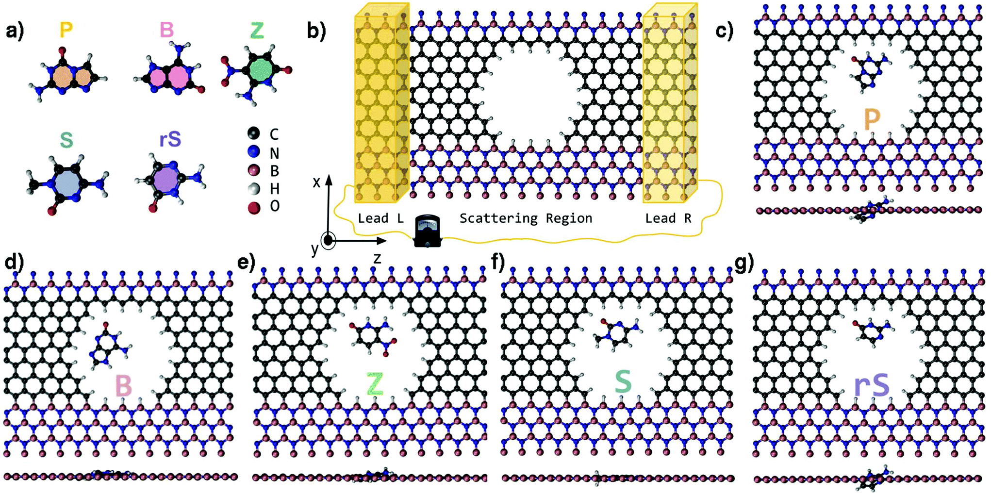 | ||
| Fig. 1 (a) The molecular structures of the Hachimoji nucleobases. (b) A sketch of the single modulation device (SMD) used to calculate electronic transport properties across an opening (nanopore). The SMD is divided into a scattering region and two leads on the left (Lead L) and the right (Lead R), respectively. (c–g) Top view and side view of the fully relaxed structures of the bare SMD filled with one of the P, B, Z, S or rS Hachimoji nucleobases. | ||
The experimental validation of unnatural genetic characters presents a challenge to label-free next-generation sequencing (NGS) techniques such as nanopore sensors.5 DNA can electrophoretically be driven through nanopores, giving rise to ionic and/or transverse currents that can be detected in real-time.6–8 Despite tremendous advances and even commercialization of sequencing devices based on biological nanopores, some experimental drawbacks need to be overcome, such as a low signal-to-noise ratio, too fast translocation speed, etc. in order to realize a label-free, rapid, and low-cost DNA sequencing through solid-state nanopores.9 In view of this scenario, nanopores in 2D materials have been pointed out as promising candidates to pave the way for the next generation of DNA sequencers.10–13 Among these, the great potential of graphene is based on its thinness,14–16 which is narrower than the distance (>0.5 nm) between two adjacent nucleotides in a single-stranded DNA (ssDNA) allowing for a single-base resolution.17,18 Accordingly, in order to assess the viability of a particular nanopore device to sequence DNA, theoretical studies have investigated the effect of each individual nucleotide within a nanopore19–21 or a nanogap-based device22–25 on transverse current signals.
In view of an enhancement of the sensitivity and the signal-to-noise ratio of bio- and gas-nanosensors, the confinement of the electronic current at a specific region in 2D-materials-based sensors has theoretically been explored as a very promising route.20,21,26–28 This confinement is expected to increase the specificity of the interaction between the sensor and the target molecule. In a graphene-based system, the electronic current pathway can theoretically be controlled by adjusting an applied gate voltage.21,29 This was proven feasible for two experimentally synthesized materials: graphene containing a topological line defect consisting of octagon and pentagon reconstructions30 and for graphene nanoroads embedded in a sheet of hexagonal-boron nitride.31 In such a nanopore context, stretching the ssDNA in the vicinity of a nanochannel has been one of the major stumbling blocks in pre-processing the molecule for genomic analysis.32 In order to resolve this, a recent computational study has presented a promising novel route to spontaneously stretch ssDNA on a h-BN nanostripe33 sandwiched between two graphene domains. Moreover, the interfacial regions within such a 2D graphene/hexagonal boron nitride (G/h-BN) material are of high importance in detection schemes. The sensitive element of this material including a nanopore is comprised of an electrically conducting carbon chain forming one edge of the nanopore. In fact, the current localized in the carbon chain adjacent to the nanopore and the h-BN is characteristically modulated by the unique dipole moment of each nucleotide passing through the nanopore.20 Motivated by the aforementioned investigations, in the setup we schematically illustrate in Fig. 1b, we place each synthetic nucleobase inside the nanodevice pore and perform electronic transport calculations in order to evaluate selectivity and sensitivity of the pore toward the synthetic nucleobases.
2. Methodology
Electronic structure calculations have been carried out based on density functional theory (DFT) as implemented in the SIESTA code.34,35 Norm-conserving Troullier–Martin pseudopotentials,36 the Perdew–Burke–Ernzerhof generalized gradient approximation (PBE-GGA)37 for exchange–correlation potential, and a double-zeta polarized (DZP) basis set38 were used in all calculations. The GGA-PBE functional has shown to describe well the hydrogen bonding compared to the more accurate MP2 and Coupled Cluster calculations.39 A real-space mesh cutoff (200 Ry) and a k-points mesh (3 × 1 × 2) in reciprocal space based on the Monkhorst–Pack scheme were applied. The conjugate gradient algorithm was employed for structural relaxations for which the cutoff for all components of the atomic forces was set to 0.01 eV Å−1.The nanopore with hydrogen-terminated edges was computationally created in a graphene ribbon embedded in h-BN. As a starting point for the geometry relaxation, each Hachimoji molecule4 depicted in Fig. 1a was separately placed inside the nanopore of the single-modulation device (SMD), so that the base plane and the plane of the device were aligned. The placement was performed in such a way to ensure that the molecular sites which participate in hydrogen bonding in a double-stranded DNA are in the vicinity of the carbon wire of the sensor device. Based on this placement, after structural optimization, each nucleobase could assume the optimal coupling geometry with respect to the carbon wire. The relaxed configurations of all target molecules inside the pore are depicted in Fig. 1c–g.
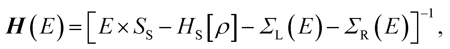
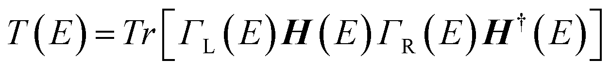
For the electronic transport calculations, the non-equilibrium Green's functions method combined with DFT was employed as implemented in Transiesta.40 We have considered the hybrid graphene/h-BN material in a supercell with dimensions 26.2 Å × 15.0 Å × 32.8 Å. This device is made up of two electrodes (left and right) and the scattering region as depicted in Fig. 1b. We have investigated the electronic transport along the z-direction. The left and right electrodes play the role of the source and drain of electrons, respectively. In order to numerically solve the large tridiagonal matrix eigenvalue problem we consider the Green's function:
 | (1) |
 | (2) |
The coupling matrices are defined as Γα = i[Σα − Σ†α], with α ≡ {L,R}. 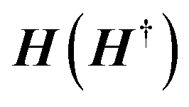 is the retarded (advanced) Green's function. Zero-bias calculations are performed in which the chemical potential of both electrodes are at the same level (μL = μR). Under this condition, the electrical current is zero by definition. Thus, our transmission calculations can be regarded as predicting the conductance of the device in the limit of small bias voltages. Further details on the theory and its numerical implementation can be found elsewhere.41,42 Note that we have assumed that during DNA translocation through the pore, the electrical signal of a particular nucleobase residing temporarily inside the pore is not affected by the adjacent nucleotides in the DNA strand.
3. Results & discussion
Inspection of all fully relaxed structures in Fig. 1c–g reveals that the B, Z, and S nucleobases remain in-plane with the device, whereas the P and rS nucleobases assume a slightly tilted conformation. As a result, the latter nucleobases exhibit a larger minimum distance (dmin) from the nanopore edges. In order to assess the energetic stability of the molecules in the device, we calculate the binding energy defined as:| Eb = ESMD+MOL − (ESMD + EMOL), | (3) |
| Nucleobase | E b (eV) | d min (Å) |
|---|---|---|
| P | +0.05 | 1.95 |
| B | −0.40 | 1.89 |
| Z | −0.02 | 1.88 |
| S | −0.19 | 1.82 |
| rS | −0.02 | 1.91 |
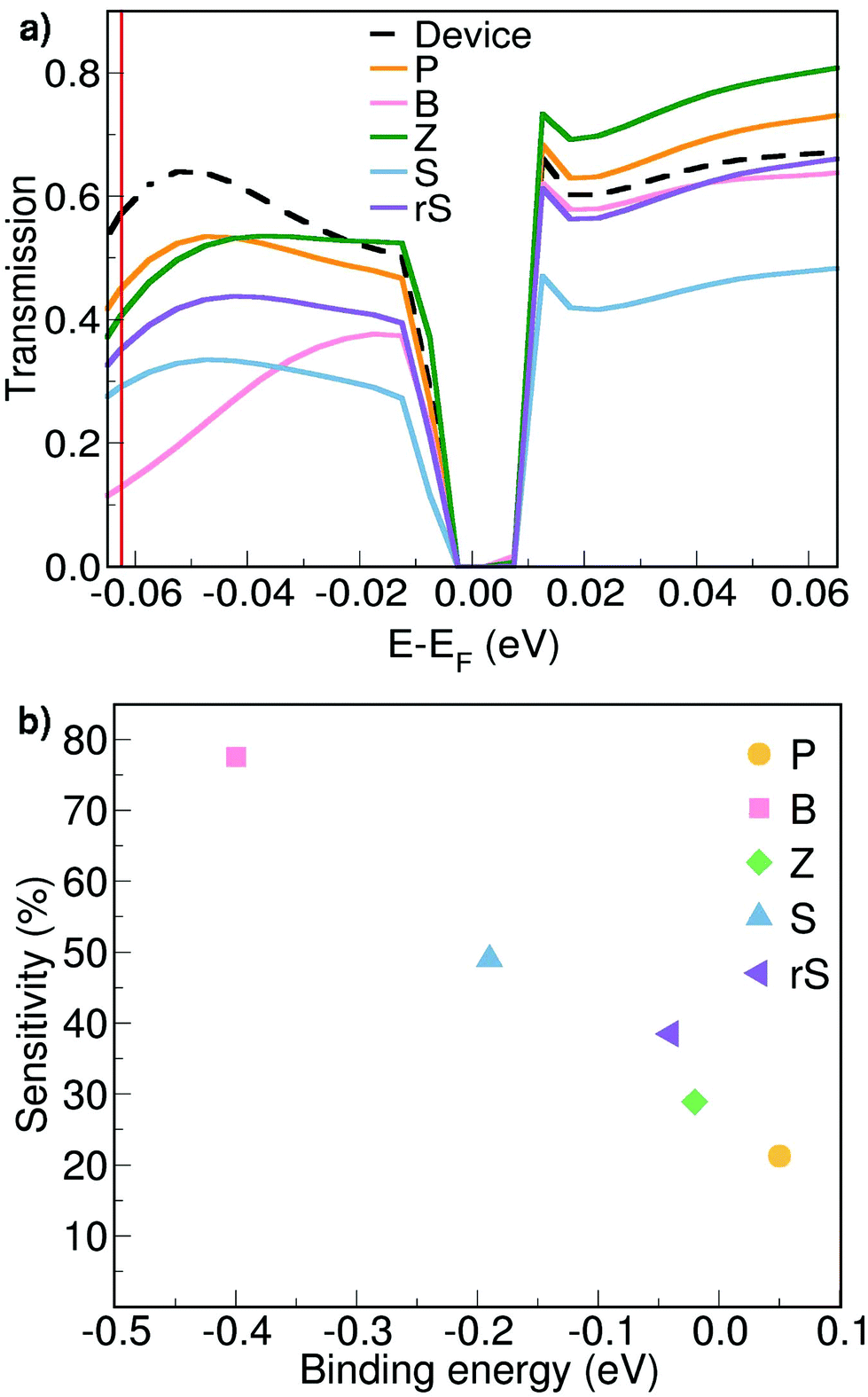
Next, electronic transport calculations are performed using the setup shown in Fig. 1b. The resulting zero-bias energy-resolved transmission spectra for a small energy interval close to the Fermi level are shown in Fig. 2a. The transmission curve of an empty pore, labelled as ‘Device’, serves as the reference to evaluate the possibility to discriminate a particular synthetic nucleobase.
 | ||
| Fig. 2 (a) Zero-bias transmission spectra for the bare device (in black) and the pore filled with each synthetic nucleobase, as denoted by the legends. (b) The sensitivity of the SMD with respect to the corresponding binding energy for each target molecule at E − EF = −0.0624 eV from panel (a). | ||
The perturbation to this reference ‘Device’ transmission curve represents the response of the SMD to the presence of the nucleobase within the pore. Virtually all transmission curves corresponding to a nucleobase in the pore exhibit a decrease with respect to the reference ‘Device’ for energy values below the Fermi level. The drop in the electronic transmission in this energy range can be assigned to the interaction of the SMD with the negatively charged sites of the target molecule (oxygen site). These are in the vicinity of the carbon wire, which creates a negative electrostatic potential and leads to the aforementioned response. The same trend has been observed for the SMD filled with natural nucleotides.20 Here, at an energy E − EF = −0.0624 eV, the transmission magnitudes follow a clear trend: Device > P > Z > rS > S > B. We will further exploit this trend in order to explain the read-out scheme according to which the proposed SMD could discriminate among all five unnatural nucleobases.
In view of such a qualitative understanding, we computationally probe our device by applying a small gate voltage (Vg) of −0.0624 V. The respective conductance is connected to the electronic transmission through the expression 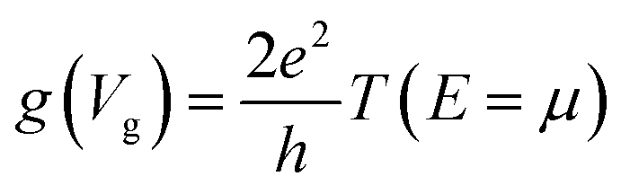 , where e is the elementary charge, h is Planck's constant and μ = EF + eVg is the chemical potential of the device.44 For a quantitative analysis of the selectivity of the SMD, we define the sensitivity as
  , where g and g0 are the conductance of the pore with a nucleobase inside and of the empty pore, respectively. The sensitivity at the applied gate voltage mentioned above as a function of the binding energy for each nucleobase is plotted in Fig. 2b. The device sensitivity shows a declining linear trend with respect to the binding energy. The sensitivity is the highest (≈80% for B) when the nucleobase is in-plane with the device and has the highest binding energy. For nucleobase P showing the weakest binding, the sensitivity reaches ≈20%, which is still significant. In spite of the fact that Z and rS have very small binding energies and are quasi not binding to the SMD, the sensitivities are large enough to allow these two molecules to be distinguished from each other. These results strongly underline the possibility to discriminate among the synthetic nucleobases. The results furthermore suggest two coupled schemes for nucleotide detection: one is based on the residence time in the pore, which is proportional to the Boltzmann factor including the binding energy (see above) and the other is based on quantifying the conductance modification due to the presence of a nucleotide. We emphasize that, thanks to this coupled scheme, even bases with similar sensitivities can be successfully distinguished, given that their binding energies are sufficiently different. Note that the smallest binding (for P) corresponds to the largest electronic transmission, but smallest current modulation as can be inferred from Fig. 2a. This more weakly bound molecule induces a smaller charge redistribution in the carbon chain of the pore edges, so that the modulation is not strongly expressed. The opposite is observed for the nucleobase with the largest binding energy (for B), which shows a much lower transmission than the SMD, but a much larger modulation as seen in Fig. 2b.
For the last part of the results, we turn to an analysis of the wavefunctions (WFs) of the systems we have studied. The WFs at an energy of E − EF = −0.0624 eV are visualized in Fig. 3. In the case of the empty pore (‘Device’) it can be observed that the WF is spread out through the left side, as well as along the carbon nanowire. The results for the nucleobase B in the pore reveal WFs slightly localized along the carbon wire. As seen in Fig. 2a, in that case, the electronic transmission is also lower than for the empty pore. The WFs for B indicate that the probability of an incoming electron from the left side to reach the right electrode is lower than in the open pore case. This decrease in the probability can be interpreted as a current modulation effect. Note, that the current is an integral over the product of the transmission and the difference of Fermi–Dirac functions. For the nucleobase S, the WFs are again less localized compared to the open pore device and slightly decreasing along the carbon wire. The behavior of the WFs for the nucleobases P, Z, and rS are similar, and again show differences compared to the bare device. Accordingly, each nucleobase inside the pore is perturbing the device, in particular the wire region. This perturbation then gives rise to the current or conductance modulation in the SMD. Note, that the transmission around the Fermi level is dominated by interface states.29
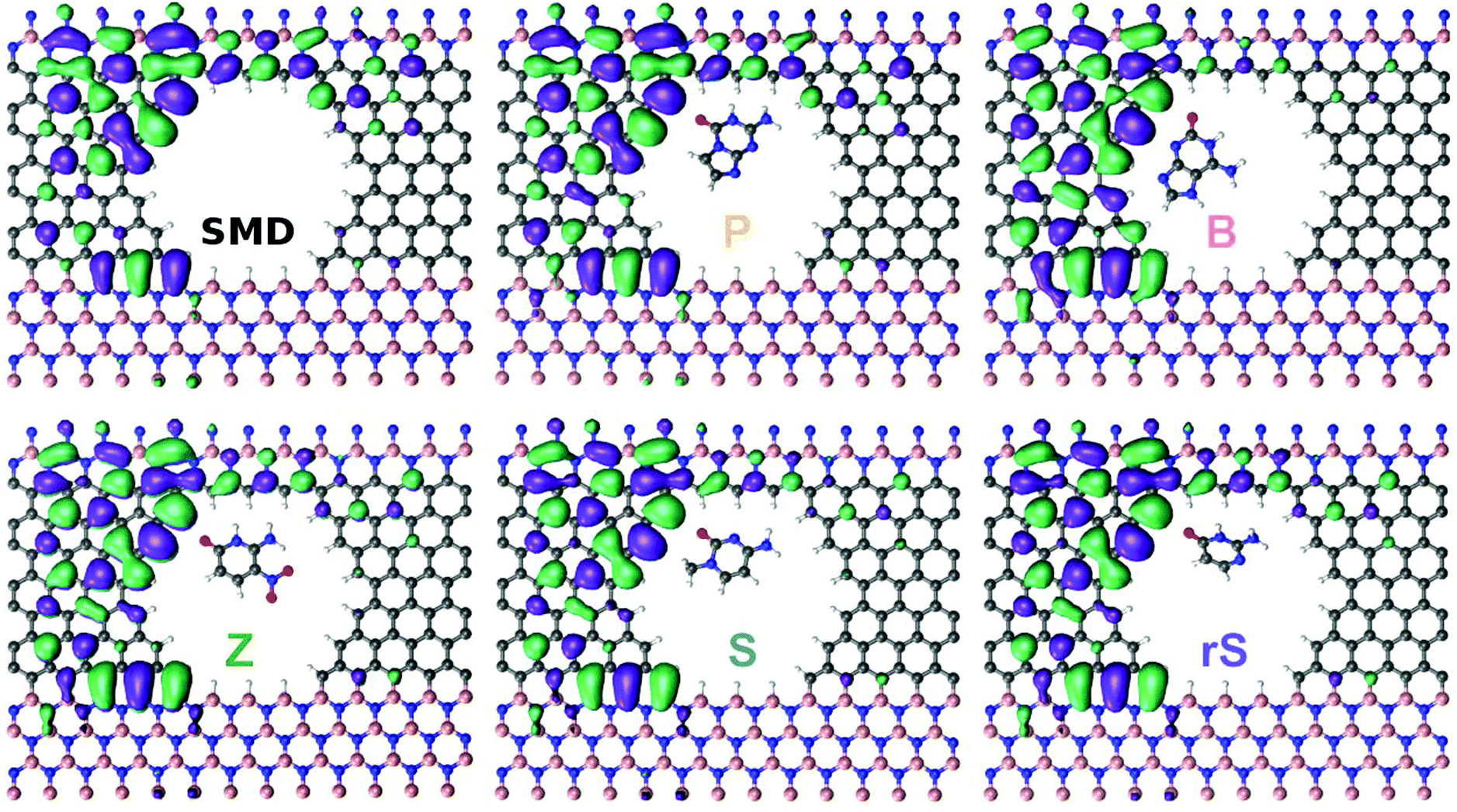 | ||
| Fig. 3 The wavefunctions corresponding to an energy of E − EF = −0.0624 eV for the bare SMD and the device filled with a synthetic nucleobase, as denoted by the labels. | ||
It must be emphasized that the proposed single modulation device represents a tremendous experimental challenge in terms of fabrication. However, this concept has the potential to pave new pathways for reducing the fluctuations of the target molecule when residing inside the pore. The device we have proposed here has one line of carbon atoms at the interface, along which the WFs of the nucleobases inside the nanopore are localized. In our simulations, the acceptor/donor atoms of the nucleobases (which would be the ones forming hydrogen bonds to a neighboring complementary nucleobase) were set to point towards the carbon nanowire. After relaxation, the structures in Fig. 1c–g represent the best coupling of the molecule towards the device. One should note though, that in a real device, an aqueous solution is present, leading to thermal fluctuations. Accordingly, further studies based on more sophisticated computational schemes, such as molecular dynamics and QM/MM methods should focus on the effect of water molecules and ions on the time-dependent configurations of the nucleobases in the pore and their respective binding to the pore. Based on previous findings,45 we do though expect that the presence of an aqueous solvent would preserve the nucleotide-specific features of the nanopore device. An additional important factor is also related to the configurational changes of the molecule within the pore. Here, we have assumed that the equilibrium configuration, the one with the best coupling between device and target molecule, will be dominant over all other possible arrangements when they are averaged out in the total transmission curve. Accordingly, we have considered only this configuration. Based on our findings, a follow-up study should also take into account other configurations of the molecules within the pore.
4. Conclusions
In summary, the main target of this work has been to computationally explore the electronic detection of the Hachimoji synthetic nucleobases in a graphene/h-BN single modulation device (SMD) containing a nanopore. The biomolecules were found to bind weakly to the SMD, indicating that they will not be trapped inside the nanopore. The zero-bias electronic transmission calculations revealed a well-resolved distinction for each artificial nucleobase through a notable associated change in the electronic transmission. The considerable differences in the sensitivities indicate a possibility of the graphene/h-BN SMD to work as a current modulation device. In such a device, local variations in the wave functions are related to nucleobase-specific probabilities of electrons to traverse from the left electrode to the right electrode through the scattering region, resulting in characteristic changes for each nucleobase. Through our model nanopore setup, we could propose two coupled schemes for identifying the synthetic nucleobases. These involve temporal measurements of the duration of a signal and conductance measurements. The former scheme is related to the residence time of the nucleobases in the pore, which exponentially depends on the binding energy through the Boltzmann factor. The latter scheme can quantify the conductance modifications (or current modulations) across the device due to the presence of the nucleotide in the pore.In the end, this work is a seminal theoretical study supporting a strong proof-of-concept that the proposed label-free biosensor-SMD with a nanopore in a heterostructure made up of graphene and h-BN has the potential to electrically discriminate synthetic DNA/RNA Hachimoji nucleobases. It is physically intuitive that in a real nanopore device, there are many more factors that influence the translocation and detection process, such as fluctuations of the 2D material, the influence of environmental factors, the existence of a long molecule with a sugar-phosphate backbone and thus linked nucleotides, and many more. However, from a fundamental theoretical point, this work has provided several interesting aspects for the potential of detecting synthetic DNA with a 2D nanopore setup. It has provided the foundation upon which future studies can gradually increase the level of complexity for more thorough investigations of the proposed device. The synthesis of in-plane heterostructures composed of graphene and h-BN with high control over the size and shape,31 the opening and control of 2D nanopores down to 1 nm,26,46 as well as the electrical detection of single nucleotides though 2D nanopores8 and the continuous exponential advancement in technological development are all reasons that culminate in the strong potential of realizing a device such as the one proposed in this work in the near future.
Conflicts of interest
There are no conflicts to declare.Acknowledgements
We gratefully acknowledge the computing resources provided on Bebop, a high-performance computing cluster operated by the Laboratory Computing Resource Center at Argonne National Laboratory. This research used resources of the Argonne Leadership Computing Facility, which is a DOE Office of Science User Facility supported under Contract DE-AC02-06CH11357. Argonne National Laboratory's work was supported by the U.S. Department of Energy, Office of Science, under contract DE-AC02-06CH11357. FALS thanks CNPq/FAPES First Projects Program for partially supporting this work (041/2019). MF acknowledges support from the collaborative network SFB 716 “Dynamic simulations of systems with large particle numbers” funded by the German Funding Agency (Deutsche Forschungsgemeinschaft, DFG) and the EXC2075 SimTech at the University of Stuttgart. RHS acknowledges financial support from the Swedish Research Council (under VR grant 2017-04627). WLS and RGA thank for financial support from CNPq (301648/2017-4 and 421227/2018-4) and (2535/2017-1 and 437182/2018-5), respectively. RGA also acknowledges financial support from the FAPERJ under grant number E-26/010.101126/2018 and 26/202.699/2019. This study was financed in part by the Coordenação de Aperfeiçoamento de Pessoal de Nível Superior – Brasil (CAPES) – Finance Code 001 and FAPES/CNPq (05/2017).References
- J. M. Berg, J. L. Tymoczko and L. Stryer, Biochemistry, W.H. Freeman, 5th edn, 2002 Search PubMed.
- J. D. Watson and F. Crick, Nature, 1953, 171, 737–738 CrossRef CAS PubMed.
- D. A. Malyshev, K. Dhami, T. Lavergne, T. Chen, N. Dai, J. M. Foster, I. R. Corrêa and F. E. Romesberg, Nature, 2014, 509, 385 CrossRef CAS PubMed.
- S. Hoshika, N. A. Leal, M.-J. Kim, M.-S. Kim, N. B. Karalkar, H.-J. Kim, A. M. Bates, N. E. Watkins, H. A. SantaLucia, A. J. Meyer, S. DasGupta, J. A. Piccirilli, A. D. Ellington, J. SantaLucia, M. M. Georgiadis and S. A. Benner, Science, 2019, 363, 884–887 CrossRef CAS PubMed.
- D. Branton, D. W. Deamer, A. Marziali, H. Bayley, S. A. Benner, T. Butler, M. Di Ventra, S. Garaj, A. Hibbs and X. Huang, et al., Nanoscience and technology: A Collection of Reviews from Nature Journals, World Scientific, 2010, pp. 261–268 Search PubMed.
- A. Meller, L. Nivon and D. Branton, Phys. Rev. Lett., 2001, 86, 3435 CrossRef CAS.
- M. Zwolak and M. Di Ventra, Rev. Mod. Phys., 2008, 80, 141 CrossRef.
- M. Graf, M. Lihter, D. Altus, S. Marion and A. Radenovic, Nano Lett., 2019, 19, 9075–9083 CrossRef CAS PubMed.
- M. Fyta, J. Phys.: Condens. Matter, 2015, 27, 273101 CrossRef PubMed.
- M. Mojtabavi, A. VahidMohammadi, W. Liang, M. Beidaghi and M. Wanunu, ACS Nano, 2019, 13, 3042–3053 CrossRef CAS PubMed.
- L. Zhou, K. Li, Z. Li, P. He, K. Lin, J. Mo and J. Ma, J. Vac. Sci. Technol., B: Nanotechnol. Microelectron.: Mater., Process., Meas., Phenom., 2019, 37, 061809 Search PubMed.
- L. Liang, F. Liu, Z. Kong, J.-W. Shen, H. Wang, H. Wang and L. Li, Phys. Chem. Chem. Phys., 2018, 20, 28886–28893 RSC.
- H. Qiu, A. Sarathy, K. Schulten and J.-P. Leburton, npj 2D Mater. Appl., 2017, 1, 3 CrossRef PubMed.
- F. Traversi, C. Raillon, S. Benameur, K. Liu, S. Khlybov, M. Tosun, D. Krasnozhon, A. Kis and A. Radenovic, Nat. Nanotechnol., 2013, 8, 939 CrossRef CAS PubMed.
- G. F. Schneider, S. W. Kowalczyk, V. E. Calado, G. Pandraud, H. W. Zandbergen, L. M. Vandersypen and C. Dekker, Nano Lett., 2010, 10, 3163–3167 CrossRef CAS PubMed.
- C. A. Merchant, K. Healy, M. Wanunu, V. Ray, N. Peterman, J. Bartel, M. D. Fischbein, K. Venta, Z. Luo and A. C. Johnson, et al. , Nano Lett., 2010, 10, 2915–2921 CrossRef CAS.
- R. H. Scheicher, A. Grigoriev and R. Ahuja, J. Mater. Sci., 2012, 47, 7439–7446 CrossRef CAS.
- J. Ambia-Garrido, A. Vainrub and B. M. Pettitt, Comput. Phys. Commun., 2010, 181, 2001–2007 CrossRef CAS PubMed.
- J. Prasongkit, G. T. Feliciano, A. R. Rocha, Y. He, T. Osotchan, R. Ahuja and R. H. Scheicher, Sci. Rep., 2015, 5, 17560 CrossRef CAS PubMed.
- F. A. de Souza, R. G. Amorim, W. L. Scopel and R. H. Scheicher, Nanoscale, 2017, 9, 2207–2212 RSC.
- J. Prasongkit, E. de Freitas Martins, F. A. De Souza, W. L. Scopel, R. G. Amorim, V. Amornkitbamrung, A. R. Rocha and R. H. Scheicher, J. Phys. Chem. C, 2018, 122, 7094–7099 CrossRef CAS.
- J. Prasongkit, A. Grigoriev, B. Pathak, R. Ahuja and R. H. Scheicher, Nano Lett., 2011, 11, 1941–1945 CrossRef CAS PubMed.
- R. G. Amorim, A. R. Rocha and R. H. Scheicher, J. Phys. Chem. C, 2016, 120, 19384–19388 CrossRef CAS.
- G. Sivaraman, R. G. Amorim, R. H. Scheicher and M. Fyta, RSC Adv., 2017, 7, 43064–43072 RSC.
- G. Sivaraman, R. G. Amorim, R. H. Scheicher and M. Fyta, Nanotechnology, 2016, 27, 414002 CrossRef PubMed.
- J. Feng, K. Liu, R. D. Bulushev, S. Khlybov, D. Dumcenco, A. Kis and A. Radenovic, Nat. Nanotechnol., 2015, 10, 1070 CrossRef CAS PubMed.
- F. A. de Souza, R. G. Amorim, J. Prasongkit, W. L. Scopel, R. H. Scheicher and A. R. Rocha, Carbon, 2018, 129, 803–808 CrossRef CAS.
- F. A. de Souza, G. Sivaraman, J. Hertkorn, R. G. Amorim, M. Fyta and W. L. Scopel, J. Mater. Chem. A, 2019, 7, 8905–8911 RSC.
- F. A. de Souza, R. G. Amorim, W. L. Scopel and R. H. Scheicher, Nanotechnology, 2016, 27, 365503 CrossRef PubMed.
- J. Lahiri, Y. Lin, P. Bozkurt, I. I. Oleynik and M. Batzill, Nat. Nanotechnol., 2010, 5, 326 CrossRef CAS PubMed.
- Z. Liu, L. Ma, G. Shi, W. Zhou, Y. Gong, S. Lei, X. Yang, J. Zhang, J. Yu and K. P. Hackenberg, et al. , Nat. Nanotechnol., 2013, 8, 119 CrossRef CAS PubMed.
- M. Shankla and A. Aksimentiev, Nat. Nanotechnol., 2019, 14, 858–865 CrossRef CAS PubMed.
- B. Luan and R. Zhou, Nat. Commun., 2019, 10, 1–6 CrossRef CAS PubMed.
- P. Hohenberg and W. Kohn, Phys. Rev. B: Solid State, 1964, 136, 864 CrossRef.
- J. M. Soler, E. Artacho, J. D. Gale, A. García, J. Junquera, P. Ordejón and D. Sánchez-Portal, J. Phys.: Condens. Matter, 2002, 14, 2745 CrossRef CAS.
- D. Hamann, M. Schlüter and C. Chiang, Phys. Rev. Lett., 1979, 43, 1494 CrossRef CAS.
- J. P. Perdew, K. Burke and M. Ernzerhof, Phys. Rev. Lett., 1996, 77, 3865 CrossRef CAS PubMed.
- J. Junquera, Ó. Paz, D. Sánchez-Portal and E. Artacho, Phys. Rev. B: Condens. Matter Mater. Phys., 2001, 64, 235111 CrossRef.
- J. Ireta, J. Neugebauer and M. Scheffler, J. Phys. Chem. A, 2004, 108, 5692–5698 CrossRef CAS.
- M. Brandbyge, J. Mozos, P. Ordejón, J. Taylor and K. Stokbro, Phys. Rev. B: Condens. Matter Mater. Phys., 2002, 65, 165401 CrossRef.
- S. Datta, Quantum transport: Atom to Transistor, Cambridge university press, 2005 Search PubMed.
- A. Rocha, V. García-Suárez, S. Bailey, C. Lambert, J. Ferrer and S. Sanvito, 2005, arXiv preprint cond-mat/0510083.
- F. A. L. de Souza, R. G. Amorim and R. H. Scheicher, et al. , Phys. Chem. Chem. Phys., 2019, 21, 24884–24890 RSC.
- S. K. Min, W. Y. Kim, Y. Cho and K. S. Kim, Nat. Nanotechnol., 2011, 6, 162 CrossRef CAS PubMed.
- M. Dou, F. C. Maier and M. Fyta, Nanoscale, 2019, 11, 14216–14225 RSC.
- J. Feng, K. Liu, M. Graf, M. Lihter, R. D. Bulushev, D. Dumcenco, D. T. Alexander, D. Krasnozhon, T. Vuletic and A. Kis, et al. , Nano Lett., 2015, 15, 3431–3438 CrossRef CAS PubMed.
Footnote |
| † All authors contributed equally to the work. |
| This journal is © The Royal Society of Chemistry 2020 |