
 Open Access Article
 This Open Access Article is licensed under a Creative Commons Attribution-Non Commercial 3.0 Unported Licence
Morphology-controlled MoS2 by low-temperature atomic layer deposition†
Chengxu
Shen
a,
Muhammad Hamid
Raza
 a,
Patrick
Amsalem
b,
Thorsten
Schultz
bc,
Norbert
Koch
bc and
Nicola
Pinna
*a
a,
Patrick
Amsalem
b,
Thorsten
Schultz
bc,
Norbert
Koch
bc and
Nicola
Pinna
*a
aInstitut für Chemie and IRIS Adlershof, Humboldt-Universität zu Berlin, Brook-Taylor-Str. 2, 12489 Berlin, Germany. E-mail: nicola.pinna@hu-berlin.de
bInstitut für Physik and IRIS Adlershof, Humboldt-Universität zu Berlin, Brook-Taylor-Str. 6, 12489 Berlin, Germany
cHelmholtz-Zentrum für Materialien und Energie GmbH, Hahn-Meitner-Platz 1, 14109 Berlin, Germany
First published on 25th September 2020
Abstract
Two-dimensional (2D) transition metal dichalcogenides (TMDs) such as MoS2 are materials for multifarious applications such as sensing, catalysis, and energy storage. Due to their peculiar charge-transport properties, it is always desired to control their morphologies from vertical nanostructures to horizontal basal-plane oriented smooth layers. In this work, we established a low-temperature ALD process for MoS2 deposition using bis(t-butylimino)bis(dimethylamino)molybdenum(VI) and H2S precursors. The ALD reaction parameters, including reaction temperature and precursor pulse times, are systematically investigated and optimized. Polycrystalline MoS2 is conformally deposited on carbon nanotubes, Si-wafers, and glass substrates. Moreover, the morphologies of the deposited MoS2 films are tuned from smooth film to vertically grown flakes, and to nano-dots, by controlling the reaction parameters/conditions. It is noticed that our MoS2 nanostructures showed morphology-dependent optical and electrocatalytic properties, allowing us to choose the required morphology for a targeted application.
Introduction
Transition metal dichalcogenides (TMDs) such as MoS2, WS2 and WSe2 are promising two-dimensional materials which have been applied in various areas due to their peculiar properties.1–3 Among TMDs, MoS2, due to its excellent electrochemical and electrical properties, has shown a great potential notably in sensors, catalysis, and transistors.1,4,5 Up to now, MoS2 is synthesized by various approaches like mechanical exfoliation,6 chemical exfoliation,7 hydrothermal methods,8 and chemical vapor deposition (CVD).9 However, these synthesis methods suffer from small particle size, poor film thickness control, and scalability.10,11 Moreover, high deposition temperature and inhomogeneous coating also limit the CVD method.1The electronic and catalytic properties of MoS2 are strongly related to its thickness and morphology. For example, bulk MoS2 exhibits an indirect bandgap of 1.2 eV, while it transits to a direct bandgap semiconductor with a 1.9 eV bandgap when it is thinned down to a monolayer,12,13 which is much more suitable for applications such as photonics, transistors,13,14 and memory devices.15 In addition, it is always desired to achieve MoS2 with high surface area or an enhanced exposure of active sites for applications in energy storage and conversion.5,16,17 Sun et al. demonstrated that flower-like MoS2 shows a better performance for Li-ion storage than MoS2 spheres.16 Ho et al. also reported the improvement in the hydrogen evolution reaction (HER) performance of MoS2 by tuning the active area.5 Therefore, it is important to develop synthesis approaches that easily allow to tune the MoS2 layer thickness, and to control the morphology and nanostructure.
Atomic layer deposition (ALD), due to its high conformality, shows great potential in the precise control of the thicknesses and morphologies of the deposited layers, especially for the preparation of complex nanostructures.1,18–23 Based on these peculiarities, several TMD nanomaterials with varying morphologies and complex nanostructures have been synthesized by ALD by modifying various deposition parameters and/or by using different substrates and templates.24–26 For example, Mattinen et al. deposited a ∼3 nm thick SnS2 film on 3D nanoscale trench substrates with a depth of 90 and a width of 30 nm.27 In another study, the morphology of the MoS2 films could be tuned from vertical nano-flakes to smooth films by controlling the sulfurization temperature of a precursor MoO3 film.25 Hämäläinen et al. also reported the vertical-growth of ReS2 on 3D substrates.26 These morphology-controlled depositions demonstrated the applicability of ALD in the synthesis of TMDs with tunable structure on various substrates.26,28
Simultaneously, researchers made a great effort on the ALD of MoS2.1,29–31 Liu et al. fabricated MoS2 with precise layer-control using MoCl5 and H2S as precursors.31 MacIsaac et al. developed an ALD/MLD process to synthesize MoS2 using Mo(CO)6 and 1,2-ethanedithiol.32 High-temperature sulfurization of thickness-controlled MoO3 by ALD is also a useful approach to obtain high-quality MoS2.10,33 Although these approaches produced promising materials, the high reaction temperatures required as well as high sulfurization temperature still hindered the progress of ALD-MoS2. Therefore, it is essential to develop an ALD process at low-temperature, which is more adaptive for temperature-sensitive substrates such as polymeric substrates and further facilitates device fabrication.1,34
Metal–amides complexes, due to their high reactivity, became a class of promising metal precursors in ALD processes for depositing high-quality metal dichalcogenides at low reaction temperatures. For example, SnS2 was prepared at 150 °C using tetrakis(dimethylamino)tin ((NMe2)4Sn),35 MoS2 was deposited even at 50 °C with tetrakis(dimethylamino)molybdenum ((NMe2)4Mo).1,34 Recently, we reported a low temperature deposition of WS2 with bis(t-butylimino)bis(dimethylamino)tungsten(VI) (BTBMW), another class of amide-containing precursors, and H2S as precursors.36 Moreover, bis(t-butylimino)bis(dimethylamino)molybdenum(VI) (BTBMMo) complex with the similar molecular structure as BTBMW has been used as molybdenum precursor for plasma-enhanced ALD or thermal-ALD synthesis of molybdenum carbonitride (MoCxNy),37 molybdenum nitride (MoN)38,39 and oxide (MoO3).40 Recently, BTBMMo was reported to be used for ALD-MoS2 by sulfurization of ALD molybdenum oxide10 and by depositing directly with the assistance of H2S plasma at a temperature above 300 °C.28 However, deposition of MoS2 using BTBMMo and H2S as precursors in a thermal ALD at low temperature (below 250 °C) with control over the morphologies and thicknesses has not been systematically investigated so far.
In this work, an ALD process of MoS2 was first established in a thermal ALD system at low temperature (<250 °C), using [(NtBu)2(NMe2)2Mo] as molybdenum precursor and H2S as a sulfur source. MoS2 was successfully deposited on Si wafers, carbon nanotubes (CNTs), and glass under optimized ALD parameters. Moreover, the influence of reaction temperature on morphologies and optical properties of ALD-MoS2 was also discussed. Further, the role of in situ post-annealing at 300 °C under H2S was investigated. Moreover, the influence of annealing temperature carried out under different environments was also studied. Finally, the potential applications for MoS2 were demonstrated by testing the catalytic properties of MoS2/CNTs nanostructures.
Experimental section
Pristine CNTs were first pretreated with nitric acid as previously reported.36 Then a CNTs dispersion was prepared by dispersing 10 mg of oxidized CNTs into 20 mL ethanol with sufficient sonication. Finally, 2 mL of the CNTs suspension was dropped cast onto a 5 × 5 cm2 aluminum foil for MoS2 ALD.The MoS2 was deposited in our homemade ALD system using bis(t-butylimino)bis(dimethylamino)molybdenum(VI) (BTBMMo, 98%, Strem), stored in a stainless steel cylinder (at 55 °C) as a molybdenum precursor. The H2S (Air Liquide, CAS number: 7783-06-4, H2S > 99.5%), kept at room temperature, was used as a source of sulfur at 400 mbar pressure. N2 (Air Liquide, 99.99%) was used as a carrier and purging gas in the ALD system to deliver the precursors and to remove the excess of the reactants and by-products, respectively. Functionalized CNTs, silicon wafers with natural oxide layer and glass were used as substrates. The ALD parameters were first optimized using silicon wafers as substrate. The ALD parameters were fixed to pulse/exposure/purge times of 1.5 s/30 s/30 s for BTBMMo and 0.2 s/75 s/30 s for H2S, respectively, unless otherwise stated. The precursors supply lines were heated to 110 °C to avoid the condensation of the metal precursor. The depositions were carried out at a chamber temperature ranging from 100–300 °C. Post annealing process, a useful approach to crystallize the deposited components, was carried out at 300 °C for 4 hours under H2S unless otherwise mentioned.
Spectroscopic ellipsometry (SENpro Sentech) was used to characterize the relative thickness of the as-deposited thin film on Si-wafer with data collection ranging from 370 to 1000 nm under a 70° incidence angle. Transmission electron microscopy (TEM, Philips CM200 LaB6) was used to characterize the morphology and structure of the as-deposited material on the CNTs. High-resolution transmission electron microscopy (HRTEM), high-angle annular dark-field scanning transmission electron microscopy (HAADF-STEM) and energy dispersive X-ray analysis (EDX) elemental mapping were measured using a FEI Talos F200S scanning/transmission electron microscope (S/TEM), operated at 200 kV. Powder X-ray diffraction (XRD) patterns were collected on a STOE Stadi MP Diffractometer with Mo Kα1 radiation source (λ = 0.7093 Å). MoS2 formation was analyzed by an XPLORA plus Raman microscope with an excitation wavelength of 532 nm laser and the Raman spectra were calibrated with the 520 cm−1 phonon mode of Si. X-ray photoelectron spectroscopy (XPS) measurements were carried out using a Jeol JPS-9030 set-up (base pressure 2.10−9 mbar) including a hemispherical energy analyzer and a monochromatic Al Kα (hv = 1486.6 eV) X-ray source in an ultrahigh vacuum chamber. For reference, the C 1s peak position from the CNTs was determined at 284.6 eV binding energy. UV-Vis spectra were recorded on a UV-Vis spectrometer (Thermo Fischer Evolution 220).
Results and discussion
In our recent report, we have developed a WS2 ALD process using the same thermal ALD system with bis(t-butylimino)bis(dimethylamino)tungsten(VI) (BTBMW) and H2S as precursors.36 Thus, by using the experience acquired with WS2 ALD, we started the MoS2 ALD experiments by adjusting the pulse/exposure/purge times as 1.5 s/30 s/30 s and 0.2 s/75 s/30 s for BTBMMo and H2S, respectively. The BTBMMo precursor was stored in a stainless steel cylinder and kept at 55 °C (keeping in view the TGA data in ref. 40) for providing sufficient vapor pressure. Finally, an in situ post-annealing process under H2S, a simple but useful approach to obtain high-quality MoS2,34 was carried out at 300 °C after the ALD process for improving the crystallinity and morphology of the deposited layers. The MoS2 deposited on Si/SiO2 wafers at 200 °C (denoted as MoS2-200) was first confirmed by Raman spectroscopy (Fig. S1a†). The two characteristic Raman peaks at 382 and 407 cm−1 are related to the in-plane (E2g1) and out of plane (A1g) vibrations of MoS2, respectively, indicating the successful synthesis of MoS2 using BTBMMo as molybdenum precursor. The large frequency difference between the two peaks (i.e., 25 cm−1) confirmed that the thickness of the MoS2 is larger than 6 layers.41Fig. S1b† shows the XRD pattern of MoS2 deposited onto the CNTs (MoS2/CNT) at 200 °C with 500 ALD cycles. The peaks at 6.27°, 14.99°, 15.34°, and 17.91° can be attributed to the (002), (100), (101) and (013) planes of MoS2 according to the reference card number COD 96-101-1287. The broad peaks are attributed to the low thickness and poor crystallinity of deposited MoS2 onto CNTs. The peak at 11.9° belongs to the (002) plane of graphitized carbon from the CNTs substrate (COD 96-101-1061). Both Raman and XRD results demonstrated the successful synthesis of MoS2 by ALD using BTBMMo and H2S as precursors.
The thermal ALD process was optimized by varying the deposition parameters, including reaction temperature and precursor pulse time (Fig. 1). Fig. 1a presents the MoS2 thickness after 200 ALD cycles as a function of the reaction temperature. A reaction with steady growth at temperatures between 100–225 °C is observed, while at higher temperatures (>225 °C) a slight increase in the growth per cycle (GPC) is recorded. Notably, this steady temperature window (100–225 °C) is close to the reported results on molybdenum oxide deposition by ALD using BMBMMo as a molybdenum precursor.42 However, due to the limitation of the temperature in our reactor, we could not study the reaction at a temperature higher than 300 °C and lower than 100 °C. Noticeably, considering the previous reports that show an ALD window using BTBMMo precursor between 260–300 °C for molybdenum nitride38 and oxide,42 suggests that the slight increase of the film thickness at 250–300 °C may not be caused by the decomposition of the metal precursor, but rather by other factors such as roughness of the deposited film (see below).28 The relationship between the MoS2 thickness after 100 ALD cycles and the pulse time of the metal precursor is presented in Fig. 1b. The substrate temperature was set to 200 °C and the pulse/exposure/purge time for H2S was kept as 0.2 s/75 s/30 s. The exposure and purge time for the metal precursor are both kept at 30 s, while the pulse time of the metal precursor was investigated in the range from 0.5 to 1.5 s with an increment of 0.25 s in each step. The layer thickness with 100 ALD cycles first increased with the increasing of the pulse time of BTBMMo and remained at ca. 7.5 nm when the dose time was longer than 1 s. This indicates that 1 s dose time for the metal precursor is sufficient to saturate the reaction chamber. However, for depositing MoS2 on high specific surface area substrates such as CNTs, we adjusted the pulse/exposure/pump time of BTBMMo and H2S at 1.5 s/30 s/30 s and 0.2 s/75 s/30 s, respectively.
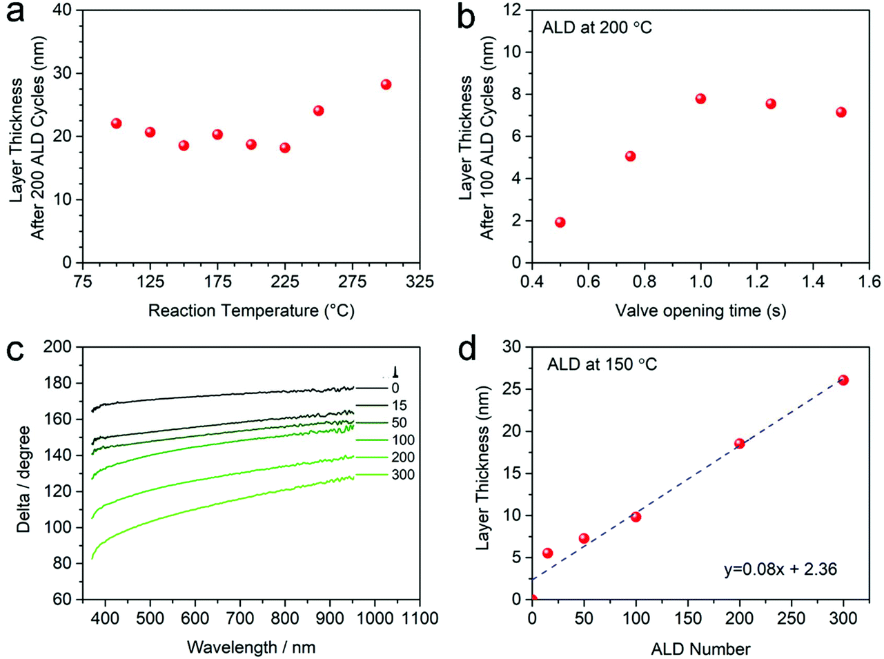 | ||
| Fig. 1 The thickness of the MoS2 as a function of the (a) deposition temperature and (b) pulse duration of BTBMMo. (c) Spectroscopic ellipsometry curves for the MoS2 deposited films with different ALD cycles (15, 50, 100, 200 and 300) at a reaction temperature of 150 °C. (d) A linear dependence between deposited film thickness and number of ALD cycles. All data sets are measured and fitted by spectroscopic ellipsometry on Si-substrates. | ||
The GPC was systematically determined by investigating the relationship between thickness and number of ALD cycles at 150 °C (Fig. 1c and d). The original data collected by spectroscopic ellipsometry on Si/SiO2 wafers are shown in Fig. 1c. It can be seen that with increasing number of ALD cycles, the curves shift to low delta values, indicating an increase in the film thickness. The shift between 0 and 15 cycles is much larger than that to the higher ALD cycle numbers, in contrast to the nucleation-inhibited reaction of WS2 reported in our previous work.36 The more probable reason for the dramatic increase of film thickness at the beginning of reaction may be due to island-like nucleation growth modes during the initial several deposition cycles.5 The film thickness increases following a linear relationship (R2 > 0.97) with a slope of 0.08 nm per cycle at 150 °C on Si wafer (Fig. 1d). Interestingly, the intercept on the y-axis demonstrates that there may be a nucleation-enhanced reaction at the beginning of the deposition. Nevertheless, the thickness and GPC value are the reference for guiding the experiment designing, the exact thickness values on different substrates should be measured by direct methods such as transmission electron microscopy.
The structure and morphologies of MoS2 deposited onto the CNTs (MoS2/CNTs), at a temperature range from 100 to 300 °C, are characterized by transmission electron microscopy (TEM). All the samples were annealed at 300 °C under H2S after the standard ALD process, except the samples that were deposited at 300 °C directly. Fig. 2 presents the overview TEM images for the samples deposited at 100, 125, 150, 175, 200, 225, 250 and 300 °C, respectively. It can be seen that the CNTs are conformally coated with a smooth film of MoS2 at relatively low temperature, i.e., 100–225 °C (Fig. 2a–f). Moreover, MoS2 deposited comparatively at lower temperatures (<150 °C) is even smoother (Fig. 2a–c) than those deposited at higher reaction temperatures, i.e., >175 °C (Fig. 2d–f). On the other hand, as the reaction temperature reached 250 °C, MoS2 deposited onto the CNTs as random nano-flakes rather than a continuous and smooth film. Noticeably, the growth model of TMDs from smooth film to vertical nano-flakes was also previously observed on planar substrates.5,26,43 Interestingly, when the reaction temperature reached 300 °C, there are only a few nanodots decorated onto CNTs, which may be due to the desorption of the molybdenum precursor from CNTs at this comparatively high temperature. On account of these results, it can be concluded that MoS2 with varying morphologies were deposited onto the CNTs by ALD through temperature-controlled processes.
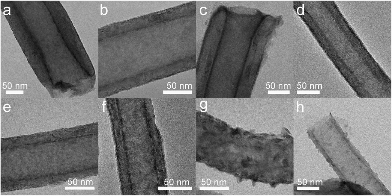 | ||
| Fig. 2 High-resolution TEM images of MoS2/CNT deposited at (a)–(g) 100, 125, 150, 175, 200, 225 and 250 °C followed by in situ post-annealing at 300 °C under H2S, and as-deposited at (h) 300 °C without post-annealing. All samples are deposited with 200 ALD cycles. | ||
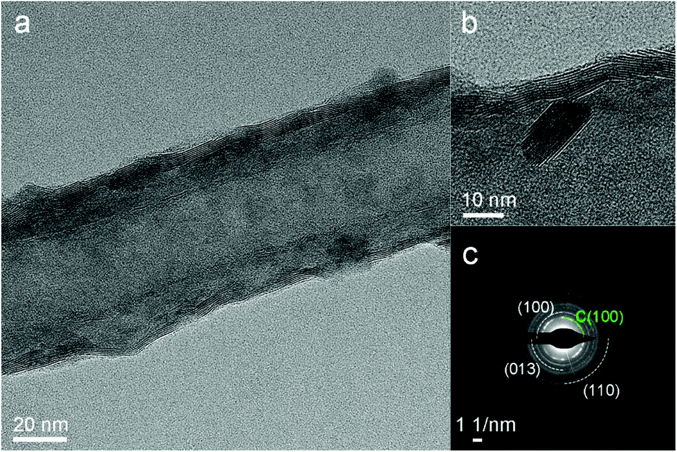
For further investigating the deposited MoS2 and the influence of the reaction temperature on their morphologies, two typical samples that were deposited at 200 °C (denoted as MoS2/CNTs-200, CNTs with smooth MoS2 coating layer) and at 250 °C (denoted as MoS2/CNTs-250, random nano-flakes grow on CNTs) were analyzed by HR-TEM, SAED and EDS elemental mappings (Fig. 3 and S2†). High-resolution TEM (HRTEM) images clearly revealed the morphologies and structures of MoS2. It can be seen that both samples are completely coated with crystalline MoS2 (Fig. 3). Noticeably, MoS2 is conformally deposited both onto the inner and outer surfaces of the CNTs with varying morphologies from smooth films to vertically grown nano-flakes for MoS2/CNTs-200 (Fig. 3a and b) and MoS2/CNTs-250 (Fig. 3e and f), respectively, further demonstrating the advantages of ALD for the conformal deposition of thin films onto the complex substrates. The HAADF-STEM and the corresponding elemental mapping images of both samples further revealed a homogenous distribution of Mo and S throughout the inner and outer walls of the CNTs, forming a smooth film of MoS2 for MoS2/CNTs-200 (Fig. 3d) and a flakes-like morphology of MoS2 for MoS2/CNTs-250 samples (Fig. 3h). The lattice fringes of 0.63 nm derived from the magnified HRTEM (red square of Fig. 3b and f) can be assigned to the (002) lattice plane for the MoS2. The selected area electron diffraction (SAED) pattern (Fig. 3c and g) of MoS2/CNTs-200 and MoS2/CNTs-250 indicate that the MoS2 coated on CNTs is polycrystalline.
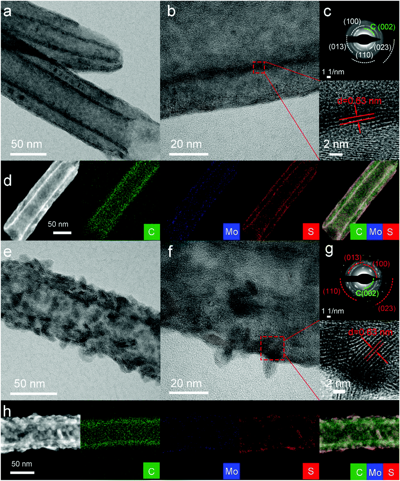 | ||
| Fig. 3 High-resolution TEM images (a and b), (e and f) and SAED (c and g) of MoS2/CNTs-200 (a–c) and MoS2/CNTs-250 (e–g). HAADF-STEM images of MoS2/CNTs-200 (d) and MoS2/CNTs-250 (h) and corresponding EDS elemental mappings. Both samples were in situ annealed at 300 °C under H2S. | ||
Concurrently, the importance of the post-annealing process is also confirmed by TEM images. Fig. S3† shows the TEM images of MoS2 deposited on CNTs at 200 and 250 °C, without post-annealing. It can be seen that the as-deposited samples at 200 °C show an amorphous MoS2 film, smoothly deposited onto the inner and outer walls of CNTs (Fig. S3a and b†), while the morphology of MoS2 deposited at 250 °C is obviously rougher than that deposited at 200 °C, indicating that the deposition temperature has a great effect on the morphology of final materials (Fig. S3d and e†). It is further noticed that the material deposited at 250 °C is a mixture of amorphous components and crystalline grains of MoS2. Several MoS2 nanocrystals are imbedded in the amorphous component, cf. the magnified view of the green dot square and the selected areas with red dot circles, Fig. S3e.† The appearance of these small MoS2 crystals is attributed to the high deposition temperature. This can analogously be observed on the samples deposited at 300 °C (Fig. S4†). Both SAED patterns indicate that the as-deposited samples are dominated by amorphous MoS2 (Fig. S3c and f†). As expected, the amorphous MoS2 film is converted to crystalline MoS2 after 4 hours post-annealing under H2S at 300 °C. Indeed, the crystalline MoS2 smoothly deposited on the surface of CNTs was confirmed by TEM data (Fig. 2 and 3).
The composition and chemical state of MoS2 deposited onto the CNTs were analyzed by X-ray photoelectron spectroscopy (XPS). The XPS data for MoS2/CNTs-200 are shown in Fig. 4a and b. The high-resolution XPS spectrum in Fig. 4a displays the Mo 3d and S 2s regions and Fig. 4b shows the S 2p region. In Fig. 4a, the peak at low binding energy at ca. 226.7 eV is due to the S 2s core level, which is followed by two distinct pairs of Mo 3d doublets. The Mo 3d5/2 from the low binding energy doublet is found at 229.0 eV and that of the high binding energy doublet is found at 232.7 eV, both doublets showing a spin–orbit splitting of ca. 3.1 eV (Fig. 4a). According to the literature, the low binding energy doublet can be readily ascribed to MoS2 and the high binding energy one to the MoO3,44 which could be mainly ascribed to the insufficient reduction of high valence Mo6+ by such a low sulfurization temperature of 300 °C, as well as the oxidation of the MoS2 film at the near-surface when it is exposed to the air. In Fig. 4b, only one S 2p doublet is found with the S 2p3/2 peak position at 162.2 eV, in agreement with the reported value of basal plane S2− ligands in MoS2.45
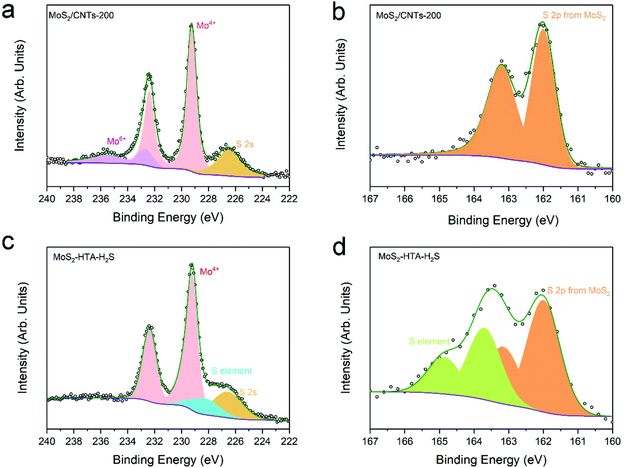 | ||
| Fig. 4 XPS spectra of Mo 3d (a and c) and S 2p (b and d) for MoS2/CNTs-200 sample, annealed in H2S at 300 °C for 4 h (a and b), and for MoS2-HTA-H2S sample, annealed in H2S at 700 °C for 2 h (c and d). | ||
Compared to the as-synthesized sample without post-annealing, the MoS2/CNTs-200 sample with post-ALD annealing under H2S shows comparatively a lower binding energy of Mo 3d5/2, which indicates a lower valence state of Mo (Fig. S5a†) demonstrating that the molybdenum has been reduced during the H2S annealing process. Moreover, the shape of the S 2p lines for the components with post-annealing at 300 °C, with a clear doublet and sharp peaks, differs strongly from that without post-sulfurization (Fig. S5b†). The latter is composed of two broad doublets, one corresponding to sulfur from MoS2 as in the sample with a post-ALD annealing process (S 2p3/2 at ca. 162 eV) and one at higher binding energy (S 2p3/2 at ca. 163.5 eV), which may be attributed to the presence elemental sulfur or amorphous MoS3.46 These results indicate that the post-annealing process is necessary to the as-deposited MoSx component for obtaining a higher quality MoS2. This is also confirmed by the high-resolution spectra of the Mo 3p–N 1s energy region (Fig. S5c†), in which the Mo 3p becomes much sharper after post-ALD annealing. Besides, no obvious N 1s signal can be observed around 400 eV both in the samples with and without post sulfurization, suggesting the complete exchange of amino and imino ligands with sulfur during the ALD process.
It can be seen that post-deposition annealing largely improved the MoS2 film (Fig. 2, 3 and Fig. S5†), even at relatively low annealing temperature, i.e., 300 °C, suggesting that a higher annealing temperature most probably will further increase the quality of ALD-MoS2. Therefore, a higher temperature sulfurization process was carried out at 700 °C under H2S flow in a tubular furnace. The sample was denoted as MoS2-HTA-H2S. The high-resolution XPS spectra in Fig. 4c and d show the Mo 3d and S 2p regions of MoS2-HTA-H2S. The Mo 3d spectrum shows only one doublet at 229.0 eV with a spin–orbit splitting of ca. 3.1 eV, which corresponds to the Mo4+ in MoS2 (Fig. 4c).44 Interestingly, the sample produced at a higher temperature sulfurization shows no signals belonging to Mo6+, compared to the 17.4% of Mo6+ in the sample of MoS2/CNT-200, which indicates that all Mo components completely convert to MoS2 during high-temperature sulfurization. The broad peak around 228.3 eV could be ascribed to elemental S, which can be further confirmed from the S 2p spectrum. There are two distinct pairs of S 2p doublets (Fig. 4d), one located at low binding energy at ca. 162.0 eV attributed to MoS2 while another located at a higher binding energy of ca. 163.7 that can be ascribed to the elemental S.47 This elemental S might be generated during the long sulfurization process under H2S at 700 °C,48 which may be controlled by reducing the sulfurization time or temperature.
The TEM images of MoS2-HTA-H2S depict the high crystallinity MoS2 film smoothly coated onto the CNTs walls (Fig. 5a and b). The SAED pattern (Fig. 5c) shows diffraction rings, which correspond to polycrystalline MoS2. The morphology of MoS2-HTA-H2S (annealed at 700 °C in H2S) is quite different from the vertical nano-flakes in MoS2/CNT-250 (Fig. 3e and f), which is in situ annealed at 300 °C under H2S. The MoS2-HTA-H2S shows a relatively smooth MoS2 film coated onto the CNTs, although there are still some nanocrystalls grown with random orientations (Fig. 5a and b). All of these results demonstrated that sulfurization at high temperatures could be a useful approach to improve the quality of as-deposited MoS2 film.
 | ||
| Fig. 5 TEM images (a and b) and SAED (c) of MoS2 deposited at 250 °C with post sulfurization under H2S atmosphere at 700 °C. | ||
Moreover, to see the effect of different annealing environments, the as-deposited samples were further annealed under forming gas (5% H2 in Ar) and inert gas (Ar) at 700 °C for 2 hours. Fig. S6† shows the TEM results of MoS2 deposited onto the CNTs at 200 °C followed by annealing at 700 °C under forming gas (denoted as MoS2-HTA-H2/Ar, Fig. S6a–c†) and under Ar (denoted as MoS2-HTA-Ar, Fig. S6d–f†) with a mass flow of 30 sccm. The HRTEM images of MoS2-HTA-H2/Ar (Fig. S6a and b†) show the presence of crystalline MoS2 film with typical lattice fringes of ∼0.63 nm, which can be ascribed to the (002) plane of MoS2 crystals. The SAED pattern (Fig. S6c†) of MoS2-HTA-H2/Ar demonstrates that the as-deposited MoS2 annealed at 700 °C under forming gas is polycrystalline. Although no obvious lattice fringes corresponding to MoS2 were observed in the MoS2-HTA-Ar sample (Fig. S6d and e†), nevertheless, the clear SAED pattern (Fig. S6f†) indicates that MoS2 is converted from amorphous to polycrystalline MoS2 during high-temperature annealing under Ar.
The optical properties of as-deposited MoS2 were investigated by UV-vis absorption spectroscopy on MoS2 deposited on glass (Fig. 6). Fig. 6a shows the UV-vis spectra of MoS2 deposited on glass at 200 °C with 100 (black), 200 (blue) and 400 (red) ALD cycles. The prominent C and D excitonic peaks around 410 nm belong to nanosized MoS2 sheets,49 while the broad and relatively lower intensity absorption peak around 600–700 nm reflects the A and B excitonic peaks derived from the K point of the Brillouin zone.50 The disappearance of distinguished A and B excitonic peaks (∼600–700 nm) may be due to the amorphous or poor crystallinity of MoS2 deposited and annealed at low temperatures.51,52 The appearance of a prominent peak around 410 nm also reflects the simultaneous existence of few-layer and nanocrystals.53 With the increase of the number of ALD cycles the absorption intensity increased significantly, which reflects the increase of mass loading of MoS2. Importantly, the absorption peaks always appeared at around 415 nm and without a significant shift. However, when the deposition temperature increased to 250 °C, the absorption peak undergoes a blue-shift from 410 to 380 nm (Fig. 6b and c). With the temperature increased to 275 °C, the absorption peak shifts to ∼370 nm. This blue-shift of the excitonic peaks may reflect the decrease of the nanocrystal size,49,53 as confirmed from TEM measurements. Furthermore, as the reaction temperature decreased to 100 °C, the absorption peak also shows a tendency to blue-shift with a ∼15 nm wavelength range (Fig. 6c).
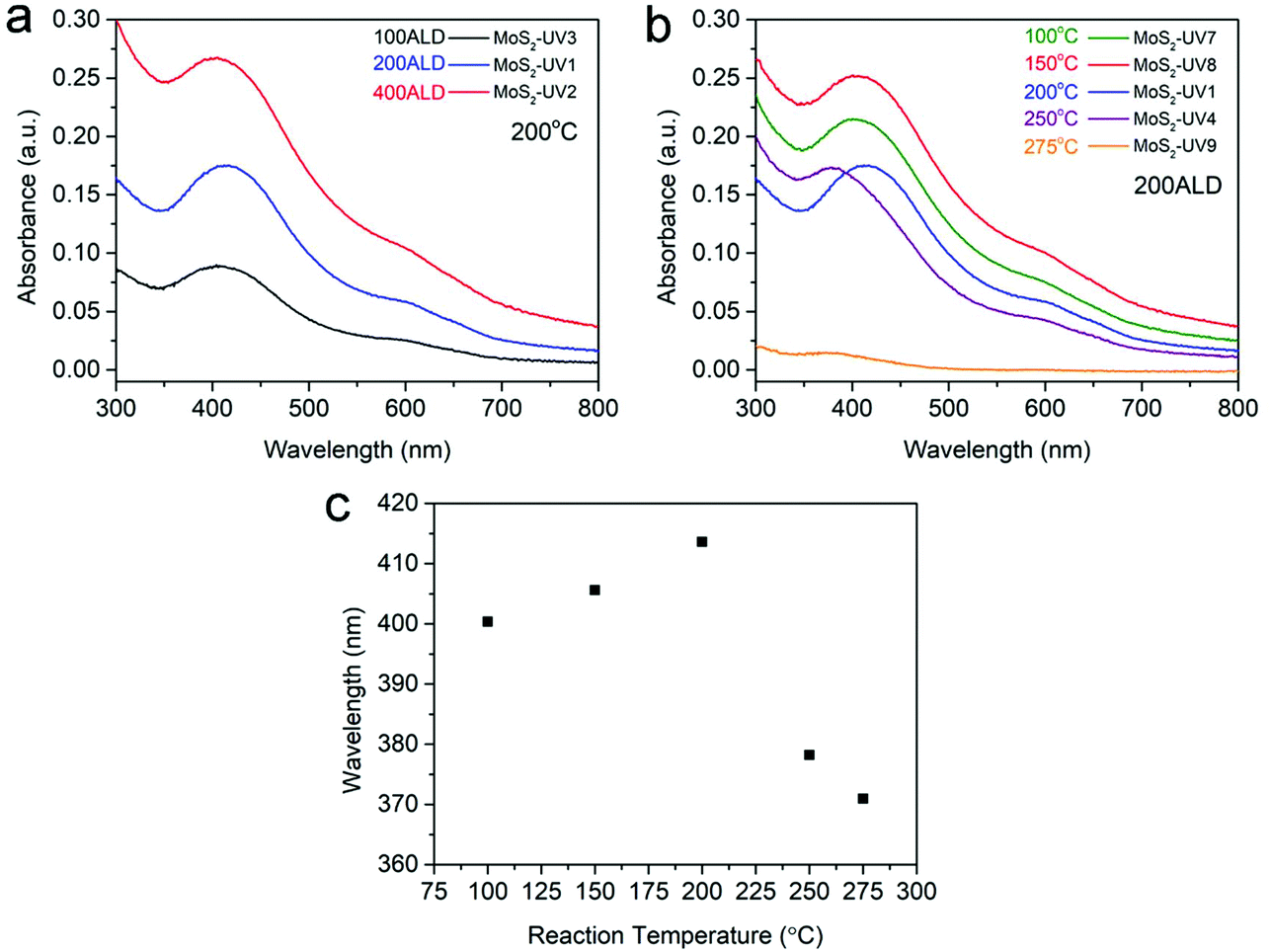 | ||
| Fig. 6 UV-vis spectra of MoS2 deposited on glass at 200 °C for different numbers of ALD cycles (a) and at different reaction temperatures with 200 ALD cycles (b). Variation of the wavelength of the absorption peak as a function of the reaction temperature (c). All the samples are post-sulfurized under a H2S atmosphere at 300 °C. | ||
As discussed in the introduction, different applications require specific characteristics of the TMDs materials in terms of morphology, nanostructure and film thickness. For example, smooth and even few-layer films of TMDs are much more suitable for semiconductor applications due to their tunable bandgap via controlling the film thickness, while TMDs with flake-like morphologies are more suitable for energy and catalysis applications, because of their high specific surface area and more exposed edges along with active sites.26 It is reported that few-layer exfoliated MoS2 presented high selectivity in gas sensors,4 while flower-liked MoS2 exhibited excellent HER performance.54 As an example of applications for our MoS2/CNTs synthesized heterostructure, HER measurements are briefly presented (Fig. S7†). Undoubtedly, the MoS2/CNTs-250 sample shows a comparatively lower overpotential at current densities of 10 mA cm−2 than the MoS2/CNTs-200 sample due to the exposed nanoflakes, which provide more catalytic active sites.
Conclusions
In summary, we report a successful deposition of MoS2 by thermal ALD at a low reaction temperature, using bis(t-butylimino)bis(dimethylamino)molybdenum(VI) (BTBMMo) and H2S as a Mo precursor and sulfur source, respectively. The MoS2 has been deposited onto different substrates including Si-wafer, CNTs and glass, where the morphologies of the MoS2 film were controlled from smooth film to vertical nanoflakes, and to nanodots by controlling the ALD reaction temperature and post-ALD annealing steps. The influence of annealing temperature and environments on the quality of final MoS2 films are also studied systematically. Moreover, the optical properties and the electrocatalytic activities of the MoS2 films show noticeable dependence on the morphology of the MoS2 nanostructures. As a matter of fact, vertically grown MoS2 flakes show a comparatively higher HER performance than the smoothly deposited MoS2 thin films, because of the higher surface area and surface concentration of catalytically active sites. All in all, we believe that the advantages and practical applications of such a facile low-temperature ALD process for morphology-controlled MoS2 thin films will enhance its potential applicability in electronics, catalysis and sensing devices.Conflicts of interest
There is no conflict of interest to declare.Acknowledgements
C. Shen acknowledges the fellowship from the China Scholarship Council (CSC). The authors thank C. Erdmann for performing the electron microscopy measurements. This work was partially funded by the Deutsche Forschungsgemeinschaft (DFG) – Projektnummer PI 762/11-1 and Projektnummer 182087777 – SFB 951.References
- T. Jurca, M. J. Moody, A. Henning, J. D. Emery, B. Wang, J. M. Tan, T. L. Lohr, L. J. Lauhon and T. J. Marks, Angew. Chem., Int. Ed., 2017, 56, 4991–4995 CrossRef CAS.
- B. Groven, M. Heyne, A. Nalin Mehta, H. Bender, T. Nuytten, J. Meersschaut, T. Conard, P. Verdonck, S. Van Elshocht, W. Vandervorst, S. De Gendt, M. Heyns, I. Radu, M. Caymax and A. Delabie, Chem. Mater., 2017, 29, 2927–2938 CrossRef CAS.
- T. Dai, Y. Liu, X. Liu, D. Xie and Y. Li, J. Alloys Compd., 2019, 785, 951–957 CrossRef CAS.
- F. K. Perkins, A. L. Friedman, E. Cobas, P. M. Campbell, G. G. Jernigan and B. T. Jonker, Nano Lett., 2013, 13, 668–673 CrossRef CAS.
- T. A. Ho, C. Bae, S. Lee, M. Kim, J. M. Montero-Moreno, J. H. Park and H. Shin, Chem. Mater., 2017, 29, 7604–7614 CrossRef CAS.
- D. Wang, F. Wu, Y. Song, C. Li and L. Zhou, J. Alloys Compd., 2017, 728, 1030–1036 CrossRef CAS.
- Q. Ding, F. Meng, C. R. English, M. Caban-Acevedo, M. J. Shearer, D. Liang, A. S. Daniel, R. J. Hamers and S. Jin, J. Am. Chem. Soc., 2014, 136, 8504–8507 CrossRef CAS.
- Y. Peng, Z. Meng, C. Zhong, J. Lu, W. Yu, Y. Jia and Y. Qian, Chem. Lett., 2001, 30, 772–773 CrossRef.
- A. Sanne, R. Ghosh, A. Rai, M. N. Yogeesh, S. H. Shin, A. Sharma, K. Jarvis, L. Mathew, R. Rao, D. Akinwande and S. Banerjee, Nano Lett., 2015, 15, 5039–5045 CrossRef CAS.
- B. D. Keller, A. Bertuch, J. Provine, G. Sundaram, N. Ferralis and J. C. Grossman, Chem. Mater., 2017, 29, 2024–2032 CrossRef CAS.
- X. Wang and G. Yushin, Energy Environ. Sci., 2015, 8, 1889–1904 RSC.
- A. Splendiani, L. Sun, Y. Zhang, T. Li, J. Kim, C. Y. Chim, G. Galli and F. Wang, Nano Lett., 2010, 10, 1271–1275 CrossRef CAS.
- B. Radisavljevic, A. Radenovic, J. Brivio, V. Giacometti and A. Kis, Nat. Nanotechnol., 2011, 6, 147–150 CrossRef CAS.
- B. W. Baugher, H. O. Churchill, Y. Yang and P. Jarillo-Herrero, Nano Lett., 2013, 13, 4212–4216 CrossRef CAS.
- S. Bertolazzi, D. Krasnozhon and A. Kis, ACS Nano, 2013, 7, 3246–3252 CrossRef CAS.
- P. Sun, W. Zhang, X. Hu, L. Yuan and Y. Huang, J. Mater. Chem. A, 2014, 2, 3498–3504 RSC.
- W. Wu, C. Niu, C. Wei, Y. Jia, C. Li and Q. Xu, Angew. Chem., Int. Ed., 2019, 58, 2029–2033 CrossRef CAS.
- C. Marichy, M. Bechelany and N. Pinna, Adv. Mater., 2012, 24, 1017–1032 CrossRef CAS.
- W. Jeon, Y. Cho, S. Jo, J. H. Ahn and S. J. Jeong, Adv. Mater., 2017, 29, 1703031 CrossRef.
- N. Pinna and M. Knez, Atomic layer deposition of nanostructured materials, Wiley-VCH, 2012 Search PubMed.
- A. Pucci, C. Marichy, M. G. Willinger and N. Pinna, in Atomic layer deposition of nanostructured materials, Wiley-VCH, 2012, DOI:10.1002/9783527639915.ch14.
- M. H. Raza, K. Movlaee, S. G. Leonardi, N. Barsan, G. Neri and N. Pinna, Adv. Funct. Mater., 2020, 30, 1906874 CrossRef CAS.
- M. H. Raza, N. Kaur, E. Comini and N. Pinna, ACS Appl. Mater. Interfaces, 2020, 12, 4594–4606 CrossRef CAS.
- S. B. Basuvalingam, Y. Zhang, M. A. Bloodgood, R. H. Godiksen, A. G. Curto, J. P. Hofmann, M. A. Verheijen, W. M. M. Kessels and A. A. Bol, Chem. Mater., 2019, 31, 9354–9362 CrossRef CAS.
- R. I. Romanov, M. G. Kozodaev, D. I. Myakota, A. G. Chernikova, S. M. Novikov, V. S. Volkov, A. S. Slavich, S. S. Zarubin, P. S. Chizhov, R. R. Khakimov, A. A. Chouprik, C. S. Hwang and A. M. Markeev, ACS Appl. Nano Mater., 2019, 2, 7521–7531 CrossRef CAS.
- J. Hämäläinen, M. Mattinen, K. Mizohata, K. Meinander, M. Vehkamaki, J. Raisanen, M. Ritala and M. Leskela, Adv. Mater., 2018, 30, e1703622 CrossRef.
- M. Mattinen, P. J. King, L. Khriachtchev, K. Meinander, J. T. Gibbon, V. R. Dhanak, J. Raisanen, M. Ritala and M. Leskela, Small, 2018, 14, e1800547 CrossRef.
- A. Sharma, M. A. Verheijen, L. Wu, S. Karwal, V. Vandalon, H. C. M. Knoops, R. S. Sundaram, J. P. Hofmann, W. Kessels and A. A. Bol, Nanoscale, 2018, 10, 8615–8627 RSC.
- Z. Jin, S. Shin, D. H. Kwon, S. J. Han and Y. S. Min, Nanoscale, 2014, 6, 14453–14458 RSC.
- D. K. Nandi, S. Sahoo, S. Sinha, S. Yeo, H. Kim, R. N. Bulakhe, J. Heo, J. J. Shim and S. H. Kim, ACS Appl. Mater. Interfaces, 2017, 9, 40252–40264 CrossRef CAS.
- L. Liu, Y. Huang, J. Sha and Y. Chen, Nanotechnology, 2017, 28, 195605 CrossRef.
- C. MacIsaac, J. R. Schneider, R. G. Closser, T. R. Hellstern, D. S. Bergsman, J. Park, Y. Liu, R. Sinclair and S. F. Bent, Adv. Funct. Mater., 2018, 28, 1800852 CrossRef.
- M. L. Shi, L. Chen, T. B. Zhang, J. Xu, H. Zhu, Q. Q. Sun and D. W. Zhang, Small, 2017, 13, 1603157 CrossRef.
- S. Cadot, O. Renault, M. Fregnaux, D. Rouchon, E. Nolot, K. Szeto, C. Thieuleux, L. Veyre, H. Okuno, F. Martin and E. A. Quadrelli, Nanoscale, 2017, 9, 538–546 RSC.
- G. Ham, S. Shin, J. Park, H. Choi, J. Kim, Y. A. Lee, H. Seo and H. Jeon, ACS Appl. Mater. Interfaces, 2013, 5, 8889–8896 CrossRef CAS.
- Y. Wu, M. H. Raza, Y.-C. Chen, P. Amsalem, S. Wahl, K. Skrodczky, X. Xu, K. S. Lokare, M. Zhukush, P. Gaval, N. Koch, E. A. Quadrelli and N. Pinna, Chem. Mater., 2019, 31, 1881–1890 CrossRef CAS.
- A. Bertuch, B. D. Keller, N. Ferralis, J. C. Grossman and G. Sundaram, J. Vac. Sci. Technol., A, 2017, 35, 01B141 CrossRef.
- V. Miikkulainen, M. Suvanto and T. A. Pakkanen, Chem. Mater., 2007, 19, 263–269 CrossRef CAS.
- V. Miikkulainen, M. Suvanto, T. A. Pakkanen, S. Siitonen, P. Karvinen, M. Kuittinen and H. Kisonen, Surf. Coat. Technol., 2008, 202, 5103–5109 CrossRef CAS.
- A. Bertuch, G. Sundaram, M. Saly, D. Moser and R. Kanjolia, J. Vac. Sci. Technol., A, 2014, 32, 01A119 CrossRef.
- C. Lee, H. Yan, L. E. Brus, T. F. Heinz, J. Hone and S. Ryu, ACS Nano, 2010, 4, 2695–2700 CrossRef CAS.
- M. F. J. Vos, B. Macco, N. F. W. Thissen, A. A. Bol and W. M. M. Kessels, J. Vac. Sci. Technol., A, 2016, 34, 01A103 CrossRef.
- M. Mattinen, T. Hatanpää, T. Sarnet, K. Mizohata, K. Meinander, P. J. King, L. Khriachtchev, J. Räisänen, M. Ritala and M. Leskelä, Adv. Mater. Interfaces, 2017, 4, 1700123 CrossRef.
- B. Kalanyan, W. A. Kimes, R. Beams, S. J. Stranick, E. Garratt, I. Kalish, A. V. Davydov, R. K. Kanjolia and J. E. Maslar, Chem. Mater., 2017, 29, 6279–6288 CrossRef CAS.
- Q. Xu, Y. Liu, H. Jiang, Y. Hu, H. Liu and C. Li, Adv. Energy Mater., 2019, 9, 1802553 CrossRef.
- Y. Shi, Y. Wang, J. I. Wong, A. Y. Tan, C. L. Hsu, L. J. Li, Y. C. Lu and H. Y. Yang, Sci. Rep., 2013, 3, 2169 CrossRef.
- A. M. de Jong, H. J. Borg, L. J. van IJzendoorn, V. G. F. M. Soudant, V. H. J. de Beer, J. A. R. van Veen and J. W. Niemantsverdriet, J. Phys. Chem., 1993, 97(24), 6477–6483 CrossRef CAS.
- Y. Lu and L. Schaefer, J. Power Sources, 2004, 135, 184–191 CrossRef CAS.
- S. Ghayeb Zamharir, R. Karimzadeh and S. H. Aboutalebi, Appl. Phys. A, 2018, 124, 692 CrossRef.
- G. Eda, H. Yamaguchi, D. Voiry, T. Fujita, M. Chen and M. Chhowalla, Nano Lett., 2011, 11, 5111–5116 CrossRef CAS.
- N. Saha, A. Sarkar, A. B. Ghosh, A. K. Dutta, G. R. Bhadu, P. Paul and B. Adhikary, RSC Adv., 2015, 5, 88848–88856 RSC.
- L. K. Tan, B. Liu, J. H. Teng, S. Guo, H. Y. Low, H. R. Tan, C. Y. Chong, R. B. Yang and K. P. Loh, Nanoscale, 2014, 6, 10584–10588 RSC.
- S. Mukherjee, R. Maiti, A. Midya, S. Das and S. K. Ray, ACS Photonics, 2015, 2, 760–768 CrossRef CAS.
- B. Gao, X. Du, Y. Ma, Y. Li, Y. Li, S. Ding, Z. Song and C. Xiao, Appl. Catal., B, 2020, 263, 117750 CrossRef CAS.
Footnote |
| † Electronic supplementary information (ESI) available. See DOI: 10.1039/d0nr03863f |
| This journal is © The Royal Society of Chemistry 2020 |