
 Open Access Article
 This Open Access Article is licensed under a
 Creative Commons Attribution 3.0 Unported Licence
Characterising the size and shape of metallic nano-structures by their acoustic vibrations†
Rafael
Fuentes-Domínguez
 *,
Shakila
Naznin
,
Leonel
Marques
,
Fernando
Pérez-Cota
,
Richard J.
Smith
and
Matt
Clark
*,
Shakila
Naznin
,
Leonel
Marques
,
Fernando
Pérez-Cota
,
Richard J.
Smith
and
Matt
Clark
Optics and Photonics Group, Faculty of Engineering, University of Nottingham, University Park, NG7 2RD, Nottingham, UK. E-mail: rafael.fuentesdominguez1@nottingham.ac.uk
First published on 24th June 2020
Abstract
The characterisation of metallic nano-structures is of great importance as their optical properties are strongly dependent on their size and shape. Inaccurate size or shape characterisation can result in misleading measurements in applications such as bio-imaging and sensing. Characterisation techniques such as dynamic light scattering, electron microscopy or atomic force microscopy are commonly used; however, performing sub-surface measurements (inside semi-transparent objects) or in liquid media are very challenging. Here, we use time-resolved pump–probe spectroscopy to characterise the size and shape of metallic nano-structures in a water surrounding medium by using their vibrational modes. We show that this technique can achieve size measurements with a precision of 3 nm for the largest nano-structures which are in agreement with electron microscopy images. Furthermore, we demonstrate the ability to probe individual nano-structures despite being located in the same optical point spread function (PSF). Combining the high precision and sub-optical measurements provided by this technique with the ability to insert metallic nano-structures inside biological samples might open a way to perform 3D characterisation measurements.
1. Introduction
Metallic nano-structures have been widely applied in bio-imaging, sensing and nonlinear optics.1–5 Accurate characterisation of these nano-structures is important since their optical and electronic properties are strongly dependent on their size and shape.6,7 Characterisation methods such as extinction measurements,8–10 direct imaging by scanning and transmission electron microscopy (SEM, TEM)11–13 and atomic force microscopy (AFM)14,15 are commonly used. However, measuring nano-structures inside a semi-transparent object or surrounded by a liquid medium is challenging as a vacuum environment and conductive substrates are needed by electron microscopy and sub-surface measurements cannot be performed by AFM.In this paper, we show that the size and shape of metallic nano-structures can be characterised by using time-resolved pump–probe spectroscopy delivered through a conventional optical microscope. The measured vibrational modes are related to the diameter, length and width of each individual nano-structure and they are compared with electron microscopy images. We are able to measure and to differentiate multiple nano-structures, with different size, under the same optical point spread function and do so with a precision of 3 nm for large particles. This provides a way to achieve sub-optical resolution imaging using the characteristic vibrations of each metallic nano-structure.16
The detection of the vibrational modes of metallic nano-structures is typically performed in a pump–probe configuration.17,18 Following the excitation by a femtosecond pump pulse, the conduction band of the metal is excited into a nonthermal electronic distribution which relaxes into thermalised electronic distribution via electron–electron interaction on the hundred femtosecond time scale.19 The hot electron gas equilibrates with the lattice via electron–phonon interaction on the picosecond time scale.20 Finally, the thermal equilibrium is reached via phonon–phonon interaction where the energy is transferred to the environment.21
Time-resolved pump–probe spectroscopy has been used to investigate the vibrational modes of different size and shape nano-structures. Nano-spheres21–23 were the first structures to be measured due to the simple fabrication and easiness to model. Later, more complicated geometries have been measured such as rods,24 triangles25 or cubes.26 With the development of electron beam-lithography (EBL), new shapes have been fabricated such as discs27 and cubes28 together with the study of their vibrational modes.
Although there has been extensive investigation of the mechanical vibrations of nano-structures, we believe that time-resolved pump–probe spectroscopy can be a key technique for the characterisation of metallic nano-structures in liquids and would be able to perform sub-surface measurements in semi-transparent objects such as biological cells. This might allow sub-optical resolution imaging of these samples where the optical labels, fluorophores, would be replaced by acoustic labels; i.e., metallic nano-structures.
2. Experimental section
2.1. Substrate preparation
A photolithography process was used to make cover-slips with reference grids for SEM purposes. A photoresist, BPRS 150, was spin-coated on a clean cover-slip and then, it was cured by ultraviolet (UV) exposure performed by a Karl Suss MJB3 Mask Aligner through the gridded mask. Later, the sample was developed by a solution (1![[thin space (1/6-em)]](https://www.rsc.org/images/entities/char_2009.gif) :8) of AZ400K and deionised (DI) water, and the cover-slip was washed with DI water and dried with nitrogen gas. Then, 10 nm of indium tin oxide (ITO) and 20 nm of gold (Au) were coated. The lift-off process was made by using warm acetone in an ultrasonic bath. Finally, an extra thin ITO film, ∼80 nm, was also coated over the entire surface before depositing the metallic nano-structures. This extra ITO layer avoids charging effects during SEM so that reference images could be taken of the nano-structures. The gridded cover-slip contained reference coordinates that were clearly visible in both optical and SEM microscopes so that the same imaging area and orientation could easily be found in all instruments.
:8) of AZ400K and deionised (DI) water, and the cover-slip was washed with DI water and dried with nitrogen gas. Then, 10 nm of indium tin oxide (ITO) and 20 nm of gold (Au) were coated. The lift-off process was made by using warm acetone in an ultrasonic bath. Finally, an extra thin ITO film, ∼80 nm, was also coated over the entire surface before depositing the metallic nano-structures. This extra ITO layer avoids charging effects during SEM so that reference images could be taken of the nano-structures. The gridded cover-slip contained reference coordinates that were clearly visible in both optical and SEM microscopes so that the same imaging area and orientation could easily be found in all instruments.
2.2. Depositing metallic nano-structures
Nano-spheres and rods were drop-coated on a homemade gridded coverslip with an electrostatic self assembly layer-by-layer process29 to avoid the nano-structures being washed away when water is added. Firstly, a layer of potassium hydroxide (KOH) solution is deposited for 1 hour on the gridded coverslip. Then, poly(allylamine hydrochloride) (PAH) and poly(styrenesulfonate) (PSS) are deposited for 30 minutes each. Between all the steps, the coverslips are washed with deionised water and dried with nitrogen.The gold spheres are 100 and 150 nm diameter (Sigma-Aldrich) with 20% polydispersity, and 125 nm (NanoPartz) with 4% polydispersity. Gold nanorods (NanoPartz) are 145 by 50 nm and 112 by 40 nm in length and width, respectively, and the polydispersity is 10%. All the previous values are provided by the manufacturer.
2.3. Experimental set-up
Time-resolved measurements are performed by a dual Ti:Sapphire (Tsunami Spectra-Physics) laser asynchronous optical sampling system (ASOPS)17,18 with ∼100 fs pulses at 80 MHz repetition rate. The ASOPS electronics allow the timing of the laser pulse from each laser to be precisely controlled and for the time delay between the pulses to be swept from 0–12.5 ns every 250 μs (4 kHz). While the lasers were wavelength tunable, these experiments were performed with fixed wavelength of 415 nm and 780 nm for the pump and probe beams, respectively.Maximum average powers of 1 mW pump and 2 mW probe (measured at sample) were used, corresponding to pulse energies of 12.5 pJ and 25 pJ, and peak powers of 125 W and 250 W, respectively. The sample was scanned in an area of 40 × 40 μm2 by moving electromechanical stages with a step-size of 0.5 μm. Both beams were focused by an objective with 0.45 NA. This produced an optical point spread function of ∼1 μm (FWHM) which limits the optical resolution to around 1 μm.
2.4. Mechanical vibrations of nano-structures
By measuring the vibrational frequencies of each metallic nano-structure using time-resolved measurements, we can extract the real size as well as shape. These vibrational modes can be described with continuous mechanics24,30 and can be used for nano-structures made of more than a few hundred of atoms.31 For a sphere, the following equation describes the main vibrational mode: | (1) |
In the case of a nano-rod with cylindrical shape,24 two main vibrational frequencies are present, along the length and the width which are referred as extensional (eqn (2)) and breathing mode (eqn (3)), respectively. These expressions are valid only if 2L/w ≫ 1, where L and w are the length and width of the rod.
 | (2) |
 | (3) |
 | (4) |
A nano-disc is equivalent to a nano-rod, but in this case, the extensional and breathing modes are along the diameter and thickness, respectively.
By knowing the mechanical properties of nano-structures which are equivalent of the bulk ones, one can extract their diameter, length and width by applying the previous equations. For the calculation of the size and shape, the following values were used for the gold nano-structures: cL = 3240 m s−1, E = 79 GPa, ρ = 19700 kg m−3 and ν = 0.42.
2.5. Finite element simulations
The previous extensional and breathing frequency expressions are only valid for a cylindrical shape rod and when the length is much larger than the width. However, this is not always the case, as rods are not perfect cylinders and their aspect ratio values might be close to 1. Therefore, finite element simulations have been performed to understand two behaviours. First, how the vibrational modes behave for different shapes and compare them with the previous analytical model. Second, what it might be possible to distinguish around AR = 1 due to frequency difference and frequency resolution of the measurements.The finite element (FE) simulations were performed using COMSOL Multiphysics 5.3a. The mechanical displacement is calculated in a 2D axial symmetry thermal stress time-dependent model and the frequency is obtained by applying a fast Fourier transform (FFT). Two geometries have been used: a ellipsoid and “real” rod shape which is composed of a cylinder and two semi-spheres at each edge. The nano-structure aspect ratios have been varied from 0.5 to 3, where each AR has the same volume, equivalent to a sphere of 100 nm diameter.
Fig. 1(a) shows both extensional and breathing mode frequencies for different rod geometries while varying the aspect ratio. The analytical model is represented by the blue line; whereas the “real” rod (a cylinder plus two semi-spheres at each edge) and the ellipsoid are the black and red line, respectively. It can be seen that the analytical model is a good approximation in the regime of AR > 1.5 which allows a fast characterisation of the experimental results. Furthermore, the main vibrational mode of a sphere is obtained when AR = 1.
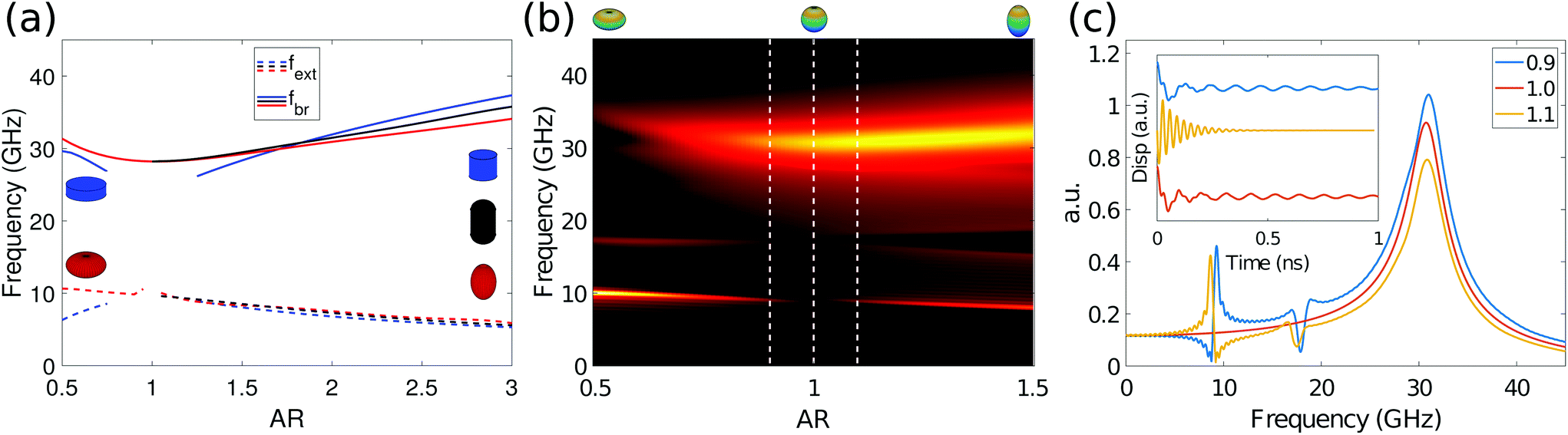 | ||
| Fig. 1 (a) Simulated extensional and breathing modes of a cylinder given by eqn (2) and (3) (blue lines) as well as the spheroid (red lines) and the “real” rod modes calculated by finite element model for different aspect ratios (AR). The geometries have constant volume and equivalent to a sphere of 100 nm diameter. (b) is the vibrational frequencies of an spheroid with volume constant calculated by finite element simulations. The white dashed lines point when AR is equal to 0.9, 1.0 and 1.1. (c) Plots the frequency traces of 0.9, 1.0 and 1.1 AR spheroid and the inset shows their time traces. These were frequency filtered to visualise the time traces in a similar way as the experimental set-up (lower frequencies are more sensitive). | ||
The full frequency spectrum of the ellipsoid from the FE simulations is shown in Fig. 1(b) where two main vibrational modes, extensional and breathing, can be seen around 10 and 30 GHz, respectively. There are some extra modes, but there are not detectable in our experiment as they are much weaker. Also, the three white dashed lines point the AR equal to 0.9, 1 and 1.1 which represents the regime where our technique cannot distinguish between a perfect sphere and a prolate or oblate spheroid. This is because the extensional mode amplitude is below the noise level. Also, the variation of the breathing mode frequency is so small, less than 0.5 GHz, that can only suggest the size change of a perfect sphere rather than a shape modification. The time and frequency traces for these aspect ratio values are shown in Fig. 1(c). The time traces were frequency filtered to visualise the traces in a similar way as the experimental set-up as the lower frequencies are more sensitive.
3. Results
Time-resolved pump–probe spectroscopy allows the study of ultrafast events in metallic nano-structures such as electron dynamics, electron–phonon coupling and phonon dynamics. The first two effects occur in a very fast regime, hundreds of femtoseconds; whereas, the phonon dynamics are from hundreds to several thousands of picoseconds. For the scope of this paper, the phonon dynamics provide all the information we need to characterise the size and shape of multiple nano-structures as we can extract their characteristic vibrational frequencies. These can be related to the real size and shape as shown in eqn (1)–(3).Representative time and frequency traces are plotted in Fig. 2(a)–(e). The frequency is extracted by a FFT after removing the electronic excitation (at t = 0) and the thermal background from the time trace. As the vibrational mode frequencies have a large range, the low frequency modes (<30 GHz) are calculated from a time trace of 0.42 ns long (blue lines); whereas, the high ones are taken from a 0.17 ns time trace (orange lines). For the case of nanorods, two main vibrational modes can be seen very clearly and due to their large aspect ratio, these frequencies are well separated. The nanorod example traces are given by a 203 × 52 nm whose frequencies are 5.15 and 45.01 GHz; and also by a 112 × 42 nm whose extensional and breathing mode are 9.06 and 55.50 GHz, respectively. Fig. 2(c) and (d) show example traces for two nano-spheres with 152 nm and 115 nm diameter where their main vibrational frequencies are 21.36 and 28.51 GHz, respectively. Finally, Fig. 2(e) shows that two frequencies are present in the same FFT; however, their values match with two nano-spheres with 138 and 102 nm (23.56 and 31.76 GHz, respectively). Although the pump laser spot is about 1 μm2, Fig. 2(e) shows two sphere vibrational modes which proves that this technique can obtain size and shape information from more than one individual nano-structure inside the same optical PSF.
 | ||
| Fig. 2 (a)–(e) are example raw time and Fourier transform traces (calculated after removing the electronic excitation and thermal background) of gold nanorods and spheres with different sizes including SEM pictures. The blue and orange lines are showing the long (0.42 ns) and short (0.17 ns) time traces used to calculate the low and high frequencies. (a) is a gold nanorod of 203 × 52 nm. (b) is a gold nanorod of 112 × 42 nm. (c) is a gold nanosphere of 152 nm. (d) is a gold nanosphere of 115 nm. (e) are two gold nanospheres of 102 and 138 nm. The insets are the SEM pictures (area of 1 μm2 and the bar is 100 nm) of the measured nano-structures where the reconstructed size and shape are drawn. | ||
All these experimental measurements match with SEM images which can be seen in the same figures. This shows that our technique agrees very well with the images taken by the electron microscope. This demonstrates that time-resolved measurements can provide the size and shape characterisation of nano-structures in a liquid surrounding medium with good agreement to SEM as well as distinguish multiple objects inside the same optical PSF.
By scanning an area with the same set-up, the size and shape characterisation of multiple metallic nano-structures is shown in Fig. 3. Each pixel of the scanned area is composed by a light intensity value (DC) and the temporal data where the vibrational modes of each nano-structure are present. The DC map (Fig. 3(a)) shows the optical image of the sample and allows the localisation of groups of nano-structures as well as defects on the specimen. From the temporal data, the vibrational frequencies can be obtained by applying a FFT as it was shown in Fig. 2. The acoustic map (or modulation depth), Fig. 3(b), is the amplitude of the largest FFT peak. Comparing the optical and acoustic maps allows the identification of any residues or defects in the sample as these can be seen optically, but they will not provide any signal in the acoustics. Furthermore, each pixel in the acoustic map can be a combination of more than one frequency, for instance, if a nano-rod or two nano-structures are present, multiple vibrational modes can coexist in the same FFT. The frequency maps were calculated by taking two different time trace lengths, 0.42 and 0.17 ns, same length as the single point measurements. The longer time trace will result in identification of the low frequency modes, i.e., the sphere and rod extensional modes shown in Fig. 3(c); whereas, for the short time trace high frequencies (rod breathing modes) will appear in Fig. 3(d).
 | ||
| Fig. 3 Size and shape characterisation data. (a) is the optical picture of a mixture of spheres and rods in an area of 40 × 40 μm2 with 0.5 μm step-size. (b) is the acoustic map. (c) is the frequency obtained by the acoustic data shown between 5 and 35 GHz (rod extensional mode and sphere main mode) and (d) is the frequency between 35 and 70 GHz (rod breathing mode). (e) Measured size and shape from as mixture of spheres (red dots) and rods (blue asterisks) given by the acoustic data. The sphere sizes are 100, 125 and 150 nm, whereas the rod length and width are 112 × 40 nm and 145 × 50 nm. The colour lines show the polydispersity of the spheres. The shaded rectangles show the polydispersity of the rods. The red dashed lines show the limitation of this technique to distinguish between a sphere and rod. | ||
The real sizes and shapes can be extracted using the frequency data from each pixel as demonstrated earlier. This is shown in Fig. 3(e) where the measured width and length of multiple spheres and rods are plotted. Here, the coloured squares are the polydispersity values for the rods given by the manufacturer (10%), whereas the lines are the size distribution for the spheres, 20% for 100 and 150 nm, and 4% for 125 nm. Furthermore, the red dashed lines point to the limitation of this technique to distinguish between a sphere and rod. This happens when the extensional mode cannot be measured due to signal-to-noise ratio (SNR) and frequency resolution, and only the breathing mode is present, seen in Fig. 1(b). We have estimated by finite element simulations that a nano-rod with aspect ratio between 0.9 and 1.1 cannot be differentiated from a sphere.
The quality factors of the scanned nano-structures shown in Fig. 3 are described here. For the range of nano-rods measured, the Q factor for the extensional and breathing mode are ∼6 and ∼8, respectively. On the other hand, the sphere Q factor is higher, around 10, and it can be seen clearly in the example traces shown in Fig. 2.
4. Discussion
The size precision and error are described in this section; however, it needs to be noticed before that the frequency spectrum is not limited by the laser repetition rate, 80 MHz. This is due to the damping of the signals which means that the frequency peaks are much wider than 80 MHz, so the peak can be located with greater precision.The frequency precision of our technique is obtained by calculating the centroid standard deviation of a simulated Gaussian (5 GHz width) with different SNR values. Although the precision is obtained from simulated data, the amplitude of the Gaussian peak and noise levels are obtained from the experimental data, giving a good approximation. Then, the frequency precision can be converted into size precision for a large rod, 200 nm, which is the worst case scenario and both are shown in Fig. 4(a). Typically, the SNR of our time-resolved system is between 10–30 which allows a frequency and size precision of ∼80 MHz and ∼3 nm, respectively, and improves when the nano-structure size is reduced. This can also be boosted by increasing the pump and probe input powers or the number of averages, despite of increasing the acquisition time.
 | ||
| Fig. 4 (a) is the frequency and size precision with respect to the SNR for a nano-structure larger than 200 nm length. (b) is the size error with respect to the frequency when the frequency error is 150 MHz. | ||
Analysis of the signals and noise in the system puts the size error to be 2.5% or 5 nm for the largest nano-structures as it is shown in Fig. 4(b). This can be obtained from the frequency error that depends on the width of the frequency peak and SNR. However, the later is the main limitation and puts the frequency error around 150 MHz for the previous experimental data. The size error is also reduced for smaller structures, 1 and 2 nm for the mean rod width and sphere size used in this paper, respectively.
However, these noise derived figures need to be treated carefully, while the measurements are repeatable to these errors, the assumptions that we have used to derive the images are slightly naive. For instance, we treat the vibration of the nano-structures as if they were suspended in free space and completely isolated from any optical or mechanical influences. The reality of the situation is that the nano-structures are sat on a hard elastic surface and the optical refractive index of the surface differs from that of water. However, this does not appear to affect our ability to measure the size and shape of these nano-structures as it is shown in the example SEM images.
The size precision and error depend on the quality factor and therefore, the surrounding medium. If the vibrations are strongly damped, the accuracy of the measurements will be reduced. However, Fig. 4 has been calculated for the worse case scenario using the range of sizes and shapes shown in Fig. 3 as well as taking into account a water surrounding medium. These values can be improved by increasing the Q factor, for instance, by using a less viscous medium like air.
The size and shape characterisation measurements can be performed in air or liquid media. There is no need for conductive substrates and the process to attach the nano-structures on the glass cover-slip does not affect the measurements. All these capabilities as well as the high precision might allow us to substitute electron microscopy by time-resolved pump–probe spectroscopy.
The current limitation of this technique is that to measure the size of two nano-structures inside the same optical PSF (1 μm2) their vibrational frequencies must be separated. In our experimental set-up, the frequency bandwidth is about ∼1.5 GHz. This is the minimum difference to be able to resolve two FFT peaks. This is equivalent to 4, 6 and 10 nm size difference for nano-spheres of 100, 125 and 150 nm, respectively. For nano-rods with 112 and 145 nm length, the minimum difference is 20 and 30 nm, respectively, whereas for a width of 40 and 50 nm, the difference is 1 and 2 nm.
The size limitation can be overcome by nano-structures with polarisation sensitive shapes such as nano-rods. In these type of nano-structures, the mechanical vibrations would be turned on and off depending on the laser polarisation which will provide a way of separating their characteristic vibrational frequencies by orientation.
Finally, others have shown that metallic nano-structures can be easily inserted in biological samples32 and can also be conjugated to target specific areas of cells. With the characterisation of the size and shape of the nano-structures with our technique, each individual structure can be super-localised providing a new way of super-resolution imaging.16 The two current limitations are the heat rise produced by the nano-structures due to the laser excitation and the UV photons used to excite the nano-structures. These two effects could damage the biological specimens as live cells are very sensitive to temperature changes as well as photo-damage. However, other shape nano-structures, such as rods, show localised plasmon resonances in the NIR regime which would allow the replacement of the UV pump laser. Also, using more sensitive nano-structures, could permit the reduction of the input power, which means less generated heat, as well as keeping a good SNR without the need of increasing the averages and in general, the acquisition time.
5. Conclusions
We have presented a technique to characterise the size and shape of metallic nano-structures by measuring their characteristic vibrational frequencies using time-resolved measurements. This technique allows us to measure nano-structures in any surrounded media, but with very high precision in agreement with electron microscopy images. The size error and precision are 5 and 3 nm, respectively, for the largest structures and the technique can localise multiple nano-structures inside the same optical PSF. Together with the possibility to insert these metallic nano-structures inside biological samples, time-resolved pump–probe spectroscopy might lead to the development of a novel super-resolution technique with acoustic resolution and the ability to do sub-surface measurements.Author contributions
Experimental concept and design: RFD, FPC, RJS and MC. Experimental measurement and analysis: RFD. Sample preparation and SEM imaging: RFD, SN and LM. All authors reviewed the manuscript.Conflicts of interest
There are no conflicts of interest to declare.Acknowledgements
This work was supported by the Engineering and Physical Sciences Research Council [grant number EP/K021877/1, EP/G061661/1]. The authors would like to acknowledge the Nanoscale and Microscale Research Centre (nmRC) at the University of Nottingham for providing access to instrumentation and SEM imaging.References
- P. Sharma, S. Brown, G. Walter, S. Santra and B. Moudgil, Adv. Colloid Interface Sci., 2006, 123, 471–485 CrossRef PubMed.
- O. S. Wolfbeis, Chem. Soc. Rev., 2015, 44, 4743–4768 RSC.
- W. Deng and E. M. Goldys, Analyst, 2014, 139, 5321–5334 RSC.
- Y.-X. Zhang and Y.-H. Wang, RSC Adv., 2017, 7, 45129–45144 RSC.
- M. Kauranen and A. V. Zayats, Nat. Photonics, 2012, 6, 737 CrossRef CAS.
- K. L. Kelly, E. Coronado, L. L. Zhao and G. C. Schatz, The optical properties of metal nanoparticles: the influence of size, shape, and dielectric environment, 2003 Search PubMed.
- I. O. Sosa, C. Noguez and R. G. Barrera, J. Phys. Chem. B, 2003, 107, 6269–6275 CrossRef CAS.
- S. K. Brar and M. Verma, TrAC, Trends Anal. Chem., 2011, 30, 4–17 CrossRef CAS.
- M. Kaasalainen, V. Aseyev, E. von Haartman, D. Ş. Karaman, E. Mäkilä, H. Tenhu, J. Rosenholm and J. Salonen, Nanoscale Res. Lett., 2017, 12, 74 CrossRef PubMed.
- A. D. Levin, E. A. Shmytkova and B. N. Khlebtsov, J. Phys. Chem. C, 2017, 121, 3070–3077 CrossRef CAS.
- E. Buhr, N. Senftleben, T. Klein, D. Bergmann, D. Gnieser, C. Frase and H. Bosse, Meas. Sci. Technol., 2009, 20, 084025 CrossRef.
- S. Yoon, B. Lee, J. Yun, J. G. Han, J.-S. Lee and J. H. Lee, Nanoscale, 2017, 9, 7114–7123 RSC.
- E. A. Grulke, X. Wu, Y. Ji, E. Buhr, K. Yamamoto, N. W. Song, A. B. Stefaniak, D. Schwegler-Berry, W. W. Burchett and J. Lambert, et al. , Metrologia, 2018, 55, 254 CrossRef CAS PubMed.
- S. Hsieh, S. Meltzer, C. C. Wang, A. A. Requicha, M. E. Thompson and B. E. Koel, J. Phys. Chem. B, 2002, 106, 231–234 CrossRef CAS.
- A. Rao, M. Schoenenberger, E. Gnecco, T. Glatzel, E. Meyer, D. Brändlin and L. Scandella, J. Phys.: Conf. Ser., 2007, 971 CrossRef CAS.
- R. Fuentes-Domínguez, F. Pérez-Cota, S. Naznin, R. J. Smith and M. Clark, Sci. Rep., 2018, 8, 16373 CrossRef PubMed.
- P. A. Elzinga, F. E. Lytle, Y. Jian, G. B. King and N. M. Laurendeau, Appl. Spectrosc., 1987, 41, 2–4 CrossRef CAS.
- A. Bartels, R. Cerna, C. Kistner, A. Thoma, F. Hudert, C. Janke and T. Dekorsy, Rev. Sci. Instrum., 2007, 78, 035107 CrossRef CAS PubMed.
- J.-Y. Bigot, V. Halté, J.-C. Merle and A. Daunois, Chem. Phys., 2000, 251, 181–203 CrossRef CAS.
- J. Hodak, I. Martini and G. V. Hartland, Chem. Phys. Lett., 1998, 284, 135–141 CrossRef CAS.
- M. Nisoli, S. De Silvestri, A. Cavalleri, A. Malvezzi, A. Stella, G. Lanzani, P. Cheyssac and R. Kofman, Phys. Rev. B: Condens. Matter Mater. Phys., 1997, 55, R13424 CrossRef CAS.
- J. H. Hodak, I. Martini and G. V. Hartland, J. Chem. Phys., 1998, 108, 9210–9213 CrossRef CAS.
- N. Del Fatti, S. Tzortzakis, C. Voisin, C. Flytzanis and F. Vallée, Phys. B, 1999, 263, 54–56 CrossRef.
- M. Hu, X. Wang, G. V. Hartland, P. Mulvaney, J. P. Juste and J. E. Sader, J. Am. Chem. Soc., 2003, 125, 14925–14933 CrossRef CAS PubMed.
- L. Bonacina, A. Callegari, C. Bonati, F. van Mourik and M. Chergui, Nano Lett., 2006, 6, 7–10 CrossRef CAS PubMed.
- H. Petrova, C.-H. Lin, S. de Liejer, M. Hu, J. M. McLellan, A. R. Siekkinen, B. J. Wiley, M. Marquez, Y. Xia and J. E. Sader, et al. , J. Chem. Phys., 2007, 126, 094709 CrossRef PubMed.
- W.-S. Chang, F. Wen, D. Chakraborty, M.-N. Su, Y. Zhang, B. Shuang, P. Nordlander, J. E. Sader, N. J. Halas and S. Link, Nat. Commun., 2015, 6, 1–8 Search PubMed.
- L. Wang, Y. Nishijima, K. Ueno, H. Misawa and N. Tamai, Appl. Phys. Lett., 2009, 95, 053116 CrossRef.
- H. Ai, S. A. Jones and Y. M. Lvov, Cell Biochem. Biophys., 2003, 39, 23–43 CrossRef CAS PubMed.
- C. Voisin, D. Christofilos, N. Del Fatti and F. Vallée, Phys. B, 2002, 316, 89–94 CrossRef.
- H. E. Sauceda, D. Mongin, P. Maioli, A. Crut, M. Pellarin, N. Del Fatti, F. Vallée and I. L. Garzón, J. Phys. Chem. C, 2012, 116, 25147–25156 CrossRef CAS.
- A. M. Alkilany and C. J. Murphy, J. Nanopart. Res., 2010, 12, 2313–2333 CrossRef CAS PubMed.
Footnote |
| † Electronic supplementary information (ESI) available: Experimental set-up diagram, additional SEMs and experimental time traces. See DOI: 10.1039/d0nr03410j |
| This journal is © The Royal Society of Chemistry 2020 |