
 Open Access Article
 This Open Access Article is licensed under a
 Creative Commons Attribution 3.0 Unported Licence
Photovoltaic nanowires affect human lung cell proliferation under illumination conditions†
Therese B.
Olsson
 ,
Laura
Abariute
,
Lukas
Hrachowina
,
Enrique
Barrigón
,
Diogo
Volpati
,
Steven
Limpert
,
Gaute
Otnes‡
,
Magnus T.
Borgström
and
Christelle N.
Prinz
*
,
Laura
Abariute
,
Lukas
Hrachowina
,
Enrique
Barrigón
,
Diogo
Volpati
,
Steven
Limpert
,
Gaute
Otnes‡
,
Magnus T.
Borgström
and
Christelle N.
Prinz
*
Division of Solid State Physics and NanoLund, Lund University, 221 00 Lund, Sweden. E-mail: christelle.prinz@ftf.lth.se
First published on 25th June 2020
Abstract
Using light to interact with cells is a promising way to steer cell behavior with minimal perturbation. Besides optogenetics, photovoltaic nanostructures such as nanowires can be used to interact with cells using light as a switch. Photovoltaic nanowires have, for instance, been used to stimulate neurons. However, the effects of the photovoltaic activity on cells are still poorly understood and characterized. Here, we investigate the effects of the photovoltaic activity of p–i–n nanowire arrays on A549 human lung adenocarcinoma cells. We have cultured A549 cells on top of vertical arrays of indium phosphide p–i–n nanowires (photovoltaic nanowires), with and without illumination to assess the effects of the nanowire photovoltaic activity on cells. We show that there is a higher proportion of dormant cells when the p–i–n nanowire arrays are illuminated. However, there is no difference in the proportion of dormant cells when the p–i–n nanowires are coated with oxide, which suggests that carrier injection in the cell medium (in this case, the release of electrons from the tip of the nanowires) is an important factor for modulating cell proliferation on photovoltaic nanowires. The results open up for interesting applications of photovoltaic nanowires in biomedicine, such as using them as a dormancy switch.
Introduction
Semiconductor nanowires are high aspect ratio nanoparticles with a diameter in the sub-100 nm scale and a length on the micron scale. They are composed of semiconductor materials, such as silicon, gallium phosphide, indium phosphide or gallium arsenide.1Vertical arrays of semiconductor nanowires have been used extensively as cell culture substrates.2,3 By tuning the geometry of the array, vertical nanowire arrays can steer cell behavior, such as motility, proliferation, morphology, and adhesion.4–9 Vertical nanowire arrays have also been used as biosensors. For instance, they have been used to record cell action potentials and measure cellular forces.10–15 In these applications, the needle-like shape of the nanowires and the versatile geometry of the array are exploited. However, semiconductor nanowire arrays exhibit functional properties beyond a compelling surface topography. For instance, above a certain diameter, nanowires act as lightguides, which can be used to integrate the fluorescent signal of biomolecules, thereby enabling analyte detection, even at very low concentrations.16–19 Moreover, semiconductor nanowires also exhibit optoelectronic properties. For instance, photoluminescent nanowires have been used to assess the biodistribution of nanowires in tissue.20–22 The optoelectronic properties of semiconductor materials can be controlled by doping (addition of impurities) during synthesis. By use of doping, nanowire heterostructures (such as p–i–n junctions) can be synthesized, which can be used as light emitting diodes, and transistors (electronical switch).23–25 For instance, nanowire field effect transistors, arranged horizontally on a substrate, have been used to detect the presence of biomolecules and record neuronal signals.26–28 Nanowires with p–i–n junctions can also exhibit photovoltaic properties, i.e. the generation of a voltage or current upon light illumination.29 Recently, photovoltaic nanowires engulfed by cells, have been used to modulate the electrical activity of neurons using light as trigger.30 In another application, silicon nanowires have been used for retinal stimulation.31 Taken together, the studies cited above suggest that combining the nanowire photovoltaic properties with array geometry effects in vertical nanowire arrays could possibly broaden the application range of nanowire arrays. However, nothing is known of the changes in cell properties when cultured on an array of photovoltaic nanowires.
Here, we assess whether the photovoltaic properties of nanowires containing a p–i–n junction can affect non-electrogenic cells cultured on an array of such nanowires. We have cultured A549 human lung adenocarcinoma cells on indium phosphide (InP) p–i–n nanowire arrays and assessed the cell properties on these substrates using immunofluorescence. Our results show that the cell viability is not affected by the photovoltaic effect. We observed a lower cell proliferation on illuminated p–i–n nanowire arrays, compared to cells seeded on non-illuminated photovoltaic nanowire arrays and illuminated non-photovoltaic nanowire arrays (referred to as inactive (InP i), in this manuscript). When the p–i–n nanowires are coated with SiO2, there is no difference in cell proliferation between illuminated and non-illuminated samples. This suggests that the injection of electrons close to the nanowire tip, in the vicinity of the cells, may be the underlying mechanism of the lower cell proliferation on uncoated p–i–n nanowires arrays.
Experimental
Nanowire synthesis
InP nanowires were grown in a low pressure (100 mbar) metal–organic vapor phase epitaxy (MOVPE) system in the vapour–liquid–solid (VLS) growth mode using H2 as the carrier gas (see below for detailed experimental protocol). Rectangular p-type InP![[thin space (1/6-em)]](https://www.rsc.org/images/entities/char_2009.gif) :Zn (111)B substrates of 9 × 11 mm2 in size were used, with a Au catalyst particle pre-defined hexagonal pattern of pitch 500 nm on the surface made using nano imprint lithography (NIL), metal evaporation and lift off.32 The Au particle dimensions were 190 nm in diameter, 70 nm in thickness. The nanowires were grown in a structure containing short p-doped bottom and n-doped top segments, with a long middle segment in between (see Fig. 1a). This middle segment was compensation-doped with Zn, with the aim of having a low enough carrier concentration for it to be depleted. This structure was chosen to maximize the volume of efficient carrier collection and hence the solar cell efficiency.33
:Zn (111)B substrates of 9 × 11 mm2 in size were used, with a Au catalyst particle pre-defined hexagonal pattern of pitch 500 nm on the surface made using nano imprint lithography (NIL), metal evaporation and lift off.32 The Au particle dimensions were 190 nm in diameter, 70 nm in thickness. The nanowires were grown in a structure containing short p-doped bottom and n-doped top segments, with a long middle segment in between (see Fig. 1a). This middle segment was compensation-doped with Zn, with the aim of having a low enough carrier concentration for it to be depleted. This structure was chosen to maximize the volume of efficient carrier collection and hence the solar cell efficiency.33
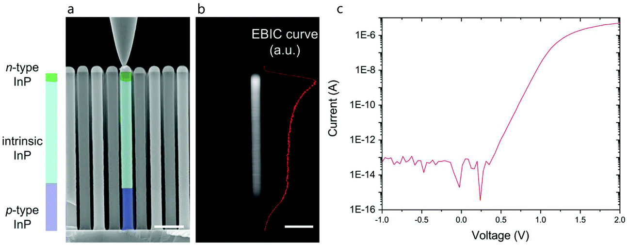 | ||
| Fig. 1 Properties of the InP p–i–n nanowires (a) schematic of a InP p–i–n nanowire next to false colored SEM image of a cross section of the InP p–i–n nanowire array. (b) EBIC profile of the InP p–i–n nanowire contacted by the nanoprobe. (c) I–V curve of the InP p–i–n nanowire contacted by the nanoprobe. Scale bars: 500 nm. | ||
InP p–i–n nanowires were grown using phosphine (PH3), trimethylindium (TMIn), diethylzinc (DEZn), and tetraethyltin (TESn) as precursors and hydrogen chloride (HCl) was used during the whole growth time (χHCl = 1.23 × 10⁻⁴) to prevent tapering by etching in situ.34 To help pattern preservation, a pre-anneal nucleation step was used, at 280 °C for 1 min under PH3 (χPH3 = 6.92 × 10⁻³), TMIn (χTMIn = 8.91 × 10⁻⁵), and DEZn (χDEZn = 8.53 × 10⁻⁶).32 Then, the temperature was raised to 550 °C and the sample was annealed for 10 min under a PH3 flow (χPH3 = 3.46 × 10⁻²) to desorb surface oxides. Subsequently, the temperature was lowered to 440 °C, the PH3 flow was decreased to its initial value (χPH3 = 6.92 × 10⁻³), and TMIn (χTMIn = 5.94 × 10⁻⁵) and DEZn (χDEZn = 1.11 × 10⁻⁵) were introduced to initiate growth of the p-segment. After 6 min and 48 s, the TMIn molar fraction was raised to χTMIn = 7.43 × 10⁻⁵ and the DEZn molar fraction was lowered to χDEZn = 9.51 × 10⁻⁸ to grow the middle segment for 23 min and 30 s. The low level of DEZn was introduced to compensate the n-type background doping of nominally intrinsic InP33 and achieve a low enough carrier concentration in the middle segment for depletion. For the n-segment, the flow of DEZn was turned off, TMIn was decreased back to χTMIn = 5.94 × 10⁻⁵, and TESn (χTESn = 4.29 × 10⁻⁵) was introduced to the chamber for 2 min. These growth conditions resulted in nanowires with a diameter of 172 ± 5 nm, a length of 2.8 ± 0.1 μm, as determined using scanning electron microscopy (SEM).
As a reference, inactive (i.e. non-photovoltaic) p-doped InP nanowires (InP i) were grown on p-type InP:Zn (111)B substrates using PH3, TMIn, DEZn and HCl as precursors using the same molar fractions as for the p-segment in the p-i-n junctions. These growth conditions resulted in nanowires with a diameter of 188 ± 10 nm, a length of 2.9 ± 0.2 μm.
For all type of arrays, an extra sample was grown as a reference to check the electrical properties of the p–i–n junctions by measuring electron beam induced current (EBIC) and I–V characteristics at the single nanowire level, using a nanoprobe system located inside the SEM33 (Fig. 1 and Fig. S1†).
Atomic layer deposition (ALD) was used to deposit 15 nm SiO2 on InP NW substrates of both p–i–n and inactive types. The deposition was performed at 150 °C using bisdiethylaminosilane (BDEAS) as precursor. The flow was set to 40 sccm for the Ar carrier gas, 40 sccm Ar and 60 sccm O2 for the plasma. Each cycle in the process consisted of 1.25 s BDEAS, 10 s Ar gas flow, 300 W plasma for 2 s and then 2 s of Ar gas flow. In total 125 cycles were performed.
Cell culture and exposure
Prior to all cell culture exposures, InP p–i–n nanowire arrays and InP i nanowire arrays were sterilized by exposing them to UV light for 10 min. Sterile nanowire array substrates were placed at the bottom of a 3.5 cm diameter Petri Dish (PD), before cells were seeded on the arrays.A549 cells (at passage #91) were purchased from European Collection of Cell Cultures (ECCC, distributor Sigma Aldrich). Cells were cultured in Ham's F12K medium (Gibco™, Scotland), containing 10% Fetal Bovine Serum (FBA, USA origin, Sigma Aldrich) and 1% penicillin–streptomycin (BioReagent, Sigma Aldrich). Cell cultures were initialized in T-75 culture flasks, at a density of 7000 cells per cm2. After cells have reached 70–80% confluence, they were passaged as follows: cells were detached from the bottom of the T-75 flask using 0.25% Trypsin-EDTA solution (BioReagent, Sigma Aldrich) for 5 min at 37 °C. The Trypsin-EDTA solution was subsequently neutralized using complete Ham's F12K medium. Cells were centrifuged for 5 min at 200g. After removing the supernatant, cells were suspended in fresh warm medium, counted, and seeded in to T-75 flask for cell culture propagation. Cells were seeded on nanowire arrays (glass substrates were used as controls) at a density of 8000 cells per cm2. All substrates were placed at the bottom of a 3.5 mm diameter PD. Immediately after cell seeding, the PD were placed in specifically designed 3D printed black boxes (Zortrax M200), preventing any external light to reach the PD, and placed in the incubator (Fig. S2a†). A commercially available, flat electroluminescent panel was glued inside the box lid; 5 cm above the substrates (see Fig. S2b† for light spectrum).
Cells were let to adhere onto the substrates and adapt to the environment for 2 hours, after which the light was turned on for 2 or 48 hours (in parallel, identical control substrates were left in the dark). Passages #94-99 were used in all experiments and each experiment was repeated at least 3 times.
Cell viability assay
The cell viability was assessed for cells cultured on InP p–i–n nanowire arrays and glass cover slips after 48 hours of incubation with/without light exposure using fluorescein diacetate (FDA, Sigma Aldrich) and propidium iodide (PI, Sigma Aldrich) according to a protocol obtained from Ibidi GmbH.35 In short, the cell medium was removed from the PD and replaced by a fresh solution of FDA (8 μg mL−1, Sigma Aldrich) and PI (20 μg mL−1, Sigma Aldrich) in Ham's F12K cell medium, without FBS and phenol red. Cells were incubated in this solution for 5 min, in the dark and at room temperature. We counterstained cells with the cell permeable dye Hoechst 33342 (1 μg mL−1), in order to count the total number of nuclei in each sample. Afterwards, cells were washed once with warm PBS, and imaged immediately in Ham's F12K medium, without FBS and phenol red, using a home built upright fluorescence microscope, optimized for high-speed multi-colour acquisitions. In this setup samples are illuminated by a LED lamp (LED4D120, Thorlabs), which is controlled by a digital controller (DC4100, Thorlabs). A 4-band filter cube (BrightLine LED-DA/FI/TR/Cy5-A-000, Semrock) is used to illuminate the sample. Fluorescent light from the sample is collected and focused by a tube lens onto the camera (Prime 95b, Photometrics). Successive triggers were used to illuminate the sample with different wavelengths (405, 470, and 530 nm).Immunohistochemistry
Cells on coverslips were mounted on a clean microscope slide with MOWIOL 4–88 solution, containing 2% DABCO anti-fading agent. The mounted samples were left to cure at room temperature in the dark overnight and stored at +4 °C for a week or at −20 °C for longer storage. Labelled cells on nanowire arrays were imaged immediately using a Nikon Ti-Eclipse microscope, using a ×10 NikonFluor objective (NA = 0.3). The nanowire arrays were placed upside down in a glass bottom PD filled with PBS and the entire sample surface area was imaged. Samples were subsequently prepared for characterization using SEM. Fluorescence microscopy images were analysed using ImageJ software.
Simulations of Au particle heating during illumination
Sequentially executed finite difference time domain (FDTD) electromagnetic wave simulations and finite element method (FEM) heat transport simulations were performed to assess the effect of the gold seed particle illumination in terms of heat. FDTD wave optics simulations of a rectangular array of InP nanowires with Au seed particles on an InP substrate with an inter-nanowire spacing of 500 nm, a nanowire length of 2.8 μm and a nanowire diameter of 200 nm, immersed in water. A single unit cell of the array surrounded by periodic boundary conditions at the x and y axis boundaries and perfectly matched layers at the z axis boundaries was simulated. Complex refractive indices of Au36 and InP37 from the literature were used. The optical power density at 500 nm was taken to be 0.1 W m−2 as determined from measurement of the experimental spectrum. The amount of power absorbed in the Au seed particle from this spectrum was computed from the FDTD simulation results and was used as the heat source in the FEM heat transport simulations. The amounts of power absorbed in the Au seed particles was found to be 2.6 × 10⁻¹⁵ W, corresponding to an absorption efficiency at 500 nm of the Au seed particles of 82%.Using the absorbed power in the Au seed particles as a heat source, finite element method (FEM) heat transport simulations of InP nanowire arrays in the case of a 300 μm thick substrate were performed. The density, specific heat and thermal conductivity of Au used were 8933 kg m−3, 385 J (kg K)−1 and 397 W (m K)−1, respectively. The density, specific heat and thermal conductivity of InP used were 4810 kg m−3, 410 J (kg K)−1 and 68 W (m K)−1, respectively. The density, specific heat and thermal conductivity of H2O used were 996 kg m−3, 4178 J (kg K)−1 and 0.6 W (m K)−1, respectively. All values were obtained from the Lumerical DEVICE software.
Scanning electron microscopy
After fluorescence imaging, the samples were dehydrated in ethanol series (20, 50, 70, 90, 95%, and absolute ethanol for 5 min). The ethanol was exchanged with liquid CO2 and the samples dried using a critical point dryer (K850, Emitech). Subsequently, the samples were sputter-coated with a 5 nm thick layer of palladium–platinum (20:80) at a 2 nm min−1 deposition rate (Sputter – Q150 T ES). SEM images of the cells were taken using a LEO-SEM 1560 at 5–15 keV acceleration voltage, using a 30 μm aperture, at a working distance of 5–10 mm, with a secondary electron detector and a 30° sample stage tilt.
Statistical analysis
The results were analysed for each group using one-way analysis of variance (ANOVA) followed by pairwise mean comparison using Tukey test. The statistical analysis was performed with OriginPro2017 (OriginLab, Northampton, MA). Statistical significance was considered at p < 0.05, p < 0.01, and p < 0.001.Results and discussion
The electrical properties of the p–i–n junctions were verified by measuring the electron beam induced current (EBIC) and I–V characteristics at the single nanowire level, using a nanoprobe system placed inside the SEM33 (Fig. 1). Fig. 1a shows a cross section SEM image of the array of InP p–i–n nanowires. The nanowire in the center of the image is being contacted by the nanoprobe and the corresponding EBIC profile is shown in Fig. 1b. The presence of an EBIC profile indicates the presence of a p–i–n junction with a signal peak at the interface between the compensation-doped middle- and top n-segment. This shows that the compensation-doped segment is actually slightly p-type, due to the introduction of Zn with the aim to balance P vacancies. Fig. 1c shows a I–V measurement of a single InP p–i–n nanowire, with a clear exponential behavior of the current as a function of voltage. The ideality factor and dark saturation current values of the diode after fitting the curve to one single diode model are 2.04 and 1.3 × 10⁻¹⁶ A, respectively. Current values lower than approximately 1 × 10⁻¹³ A are below the detection limits of the SMU employed for the measurements.Cells were cultured on InP p–i–n nanowire arrays and on glass substrates with and without illumination. After 48 h, the cell viability was assessed using fluorescein diacetate and propidium iodide (see Fig. S3† for fluorescence images of stain cells). The results show that the cell viability is not affected by the photovoltaic effect of the nanowires, i.e. there is no difference in cell viability on p–i–n nanowire arrays, whether they are illuminated or not (Fig. 2). Similarly, there are no significant differences in the proportion of apoptotic cells cultured on InP p–i–n nanowires with and without illumination (<5%, Fig. S4†). There is, however, a slight decrease in the viability of cells cultured on InP p–i–n nanowire arrays compared to when cultured on flat glass. This is in contrast with studies of cells on GaP and InAs nanowires, where the cell viability was found unaffected by the presence of nanowires.2,4,8,38 We speculate that this may be due to differences in the nanowire material. To our knowledge, nanowires made of InP have seldom been used at the interface with living cells, and no toxicity issues have been reported.15,39 In any case, since the scope of the present study is the investigation of the photovoltaic effect on cells, and as there is no difference in cell viability between cells on photovoltaic InP nanowires irrespective of the illumination conditions, we will not investigate this point further here.
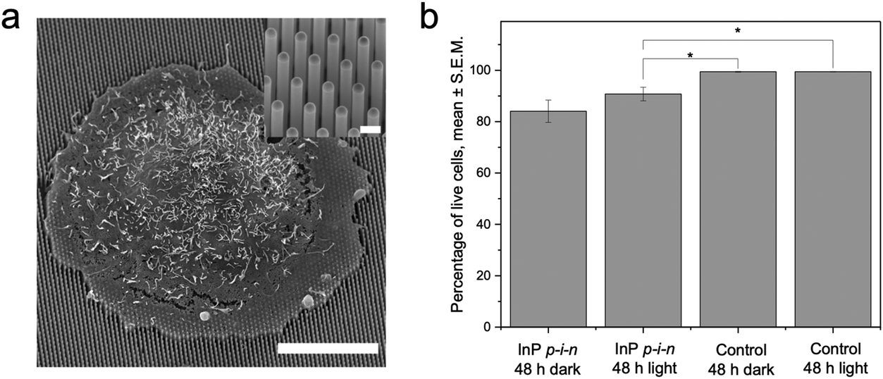 | ||
| Fig. 2 (a) SEM image of a A549 cell cultured on a InP p–i–n nanowire array substrate. Scale bars: 10 μm and 400 nm (inset) (b) percentage of live cells on InP p–i–n nanowire substrates and control glass, with and without illumination (±S.E.M.). *: p < 0.05, one-way ANOVA. n = 3, with over 450 cells counted for each condition. | ||
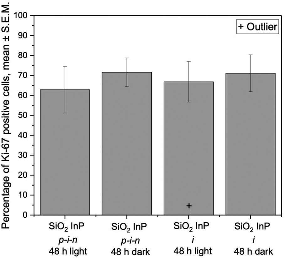
Next, we have assessed how cell proliferation varies between substrates and illumination conditions. We have stained cells for Ki-67, which labels all the cells that are in an active cell cycle phase, i.e. all phases except G0 (Fig. 3 and Fig. S5†). After 48 h, the proportion of Ki-67 positive cells is lower on illuminated photovoltaic nanowire arrays compared to on non-illuminated arrays (Fig. 3). This suggests that the photovoltaic activity of the nanowires leads to more cells being in the quiescent G0 phase of the cell cycle.
 | ||
| Fig. 3 Percentage of Ki-67 positive cells on InP p–i–n nanowire arrays, inactive InP nanowire arrays (InP i) and glass substrates (control) in the presence and absence of light (±S.E.M.). n = 11 for InP substrates, with a minimum of 1500 cells counted for each treatment; n = 9 for control substrates, with a minimum of 8000 cells counted for each condition. ***: p < 0.001, one-way ANOVA. | ||
This is comforted by the fact that cells seeded on inactive InP (InP i) nanowires (i.e. non-photovoltaic) exhibit similar proportion of Ki-67 positive cells when the substrate is illuminated compared to when left in the dark (within the error bars, Fig. 3 and Fig. S6†). The fact that the proportion of proliferating cells on glass does not vary significantly when cells are illuminated (see Fig. 3) shows that phototoxicity effects can be excluded from the list of possible explanations for the lower cell proliferation observed on illuminated photovoltaic nanowire arrays. Considering that InP i nanowires are made of the same material as InP p–i–n nanowires, we can rule out material-mediated phototoxicity as possible cause of the decreased cell proliferation. Another explanation could be that, during illumination, cells are affected by a possible heating of the Au nanoparticles, which are located on the top of the nanowires. In order to investigate this, we have performed sequentially executed finite difference time domain (FDTD) electromagnetic wave simulations and finite element method (FEM) heat transport simulations. The maximum steady state temperature in the system was recorded as a function of the illumination power density for a 500 nm illumination wavelength (Fig. S7†). At the experimental illumination power density used in this study (0.1 W m−2), for InP nanowire arrays, the maximum temperature increase was found to be 52 × 10−9 K. To achieve a steady state temperature increase of greater than 1 K, a 5 order of magnitude increase in illumination power density would be necessary. Therefore, we conclude that the illumination of the Au seed particles does not result in any substantial heating of the Au seed particles, nanowires, substrates, nor surrounding medium. Thus, it appears that the photovoltaic activity of the p–i–n nanowires is directly responsible for sending a fraction of the cells into dormancy. In InP p–i–n nanowires, illumination by light with higher energy than the bandgap creates electron–hole pairs, which are spatially separated by the built-in electric field at the p–i–n junction. For uncoated nanowires, this leads to the injection of electrons (current) in the medium at the n-doped section of the nanowires. In order to investigate whether this carrier injection may be involved in the decreased proportion of proliferating cells, we repeated the experiments on SiO2-coated InP p–i–n and inactive nanowire substrates (Fig. 4).
 | ||
| Fig. 4 Proportion of Ki-67 positive cells after 48 h culture on SiO2-coated InP p–i–n nanowires substrates and SiO2 coated InP inactive (InP i) nanowires under light and dark conditions. n = 11, with a minimum of 800 cells counted for each condition. According to one-way ANOVA statistical analysis, there are no statistical significant difference between substrates and light exposure at p < 0.05. | ||
In contrast to bare p–i–n nanowires, p–i–n nanowires coated with a dielectric material, such as SiO2, are in open circuit and build up a voltage under illumination.33 The results show no significant difference between the proportion of Ki-67 positive cells for SiO2 coated InP p–i–n and inactive nanowires, irrespective of the illumination conditions (Fig. 4). This shows that having uncoated InP p–i–n junctions releasing electrons into the medium is key in lowering the proportion of Ki-67-positive cells. Note that any significant variation in pH was not observed on the various substrates under various illumination conditions (data not shown). We cannot exclude, however, that a local pH change occurs, which would be too small to be measured in the medium.
Next, we investigated whether the effect of photovoltaic nanowires on cell proliferation is reversible. After culturing cells on illuminated InP p–i–n nanowires, the light exposure was switched off and cells were further cultured for 48 h. The results show an increase in the proportion of Ki-67 positive cells from 55 to 67% (Fig. S8†), suggesting that the photovoltaic effect on cell proliferation is, at least partly, reversible.
Finally, additional control experiments were performed. We illuminated the InP p–i–n and inactive substrates immersed in cell medium for 48 h first (without cells), and subsequently added cells in the same medium and cultured them for 48 hours in the dark. The results showed a similar proportion of Ki-67 positive cells, as for cells cultured on the substrates that were immersed in cell medium and kept in the dark for 48 h before cell seeding (Fig. S9†). Moreover, we have stained cell focal adhesions via labeling vinculin in the cells. Our results show that, while the pattern of focal adhesion differs on InP nanowires from the one of cells cultured on glass, there is no difference between the focal adhesion of cells cultured on InP p–i–n nanowire substrates with and without exposure to light (Fig. S10†).
The difference in cell and focal adhesion morphology for cells cultured on nanowires compared to cells cultured on flat substrates, with smaller cells and more point-like focal adhesion structures, has been reported before,40,41 and we show here that it is not related to the photovoltaic effect of the nanowires.
Our results point to the injection of electrons in the medium, in the direct vicinity of the cells, as being the possible underlying mechanism for the observed decrease in cell proliferation on illuminated photovoltaic nanowires. This takes place only when cells are interfacing the substrate during illumination. This effect is, at least partially, reversible after switching off the light. This opens up for exploring new applications in biomedicine. For instance, cancer cells are frequently going into dormancy when treated with chemotherapeutic compounds, which is one of the causes of cancer relapse.42 The present photovoltaic nanowires could possibly be used as a switch to induce cell dormancy while exploring new schemes to reverse or prevent cancer cell dormancy during treatment. In that context, it would be valuable to test whether the effect reported here only applies to cancer cells or is depending on the cell type. Finally, our results are also interesting from a nanosafety point of view with possible effects in skin–cell proliferation in case of contact with the skin. This particular case will be investigated in a follow-up study.
Conclusions
In summary, we have investigated the effects of culturing cells on photovoltaic InP nanowire arrays with and without illumination. Whereas the cell viability is not affected by the photovoltaic effect when the array is illuminated, the proportion of proliferating cells is substantially lower on illuminated arrays compared to when the p–i–n nanowire arrays are not illuminated. More cells in the G0 dormant phase of the cell cycle were found on the illuminated photovoltaic nanowire substrates. This effect was not observed when nanowires were coated with silicon oxide, which suggests that the injection of electrons at the cell–nanowire interface is a key factor for sending cells to a dormant state. Moreover, the fact that the proportion of proliferating cells can increase again after turning off the illumination opens up for exciting applications in biomedicine, such as using photovoltaic nanowires as switches in cell dormancy studies in the context of, for instance, cancer research.Conflicts of interest
There are no conflicts to declare.Acknowledgements
The authors would like to thank Karl Adolfsson and Martin Hjort for discussions at an early stage of the work, as well as Zhen Li, Jason Beech, Damiano Verardo and Anders Kyrsting for help with microscopy. The authors also would like to thank Dan Hessman for help with electroluminescent panel characterization. This work was financed by ERC-CoG NanoPokers, grant agreement no. 682206, Marie Sklodowska-Curie actions (656208), NanoLund, the Crafoord Foundation, MyFab, the Swedish Research Council (VR), and the Swedish Energy Agency. Nanowires were fabricated at the Lund Nano Lab. Cell critical point drying was performed at the Lund University Bioimaging Center with the help of Lina Gefors.References
- N. P. Dasgupta, J. Sun, C. Liu, S. Brittman, S. C. Andrews, J. Lim, H. Gao, R. Yan and P. Yang, Adv. Mater., 2014, 26, 2137–2183 CrossRef CAS PubMed.
- W. Hällström, T. Mårtensson, C. Prinz, P. Gustavsson, L. Montelius, L. Samuelson and M. Kanje, Nano Lett., 2007, 7, 2960–2965 CrossRef PubMed.
- Z. Li, S. Kamlund, T. Ryser, M. Lard, S. Oredsson and C. N. Prinz, J. Mater. Chem. B, 2018, 6, 7042–7049 RSC.
- G. Piret, M. T. Perez and C. N. Prinz, Biomaterials, 2013, 34, 875–887 CrossRef CAS PubMed.
- H. Persson, C. Købler, K. Mølhave, L. Samuelson, J. O. Tegenfeldt, S. Oredsson and C. N. Prinz, Small, 2013, 9, 4006–4016 CrossRef CAS PubMed.
- H. Persson, Z. Li, J. O. Tegenfeldt, S. Oredsson and C. N. Prinz, Sci. Rep., 2015, 5, 18535 CrossRef CAS PubMed.
- N. Buch-Månson, S. Bonde, J. Bolinsson, T. Berthing, J. Nygård and K. L. Martinez, Adv. Funct. Mater., 2015, 3246–3255 CrossRef.
- S. Bonde, T. Berthing, M. H. Madsen, T. K. Andersen, N. Buch-Månson, L. Guo, X. Li, F. Badique, K. Anselme, J. Nygård and K. L. Martinez, ACS Appl. Mater. Interfaces, 2013, 5, 10510–10519 CrossRef CAS PubMed.
- N. Buch-Månson, D.-H. Kang, D. Kim, K. E. Lee, M.-H. Yoon and K. L. Martinez, Nanoscale, 2017, 9, 5517–5527 RSC.
- J. T. Robinson, M. Jorgolli, A. K. Shalek, M.-H. H. Yoon, R. S. Gertner and H. Park, Nat. Nanotechnol., 2012, 7, 180–184 CrossRef CAS PubMed.
- X. J. Duan, R. X. Gao, P. Xie, T. Cohen-Karni, Q. Qing, H. S. Choe, B. Z. Tian, X. C. Jiang and C. M. Lieber, Nat. Nanotechnol., 2012, 7, 174–179 CrossRef CAS PubMed.
- W. Hällström, M. Lexholm, D. B. Suyatin, G. Hammarin, D. Hessman, L. Samuelson, L. Montelius, M. Kanje and C. N. Prinz, Nano Lett., 2010, 10, 782–787 CrossRef PubMed.
- Z. Li, H. Persson, K. Adolfsson, L. Abariute, M. T. Borgström, D. Hessman, K. Åström, S. Oredsson and C. N. Prinz, Nanoscale, 2017, 9, 19039–19044 RSC.
- Z. Li, J. H. Song, G. Mantini, M. Y. Lu, H. Fang, C. Falconi, L. J. Chen and Z. L. Wang, Nano Lett., 2009, 9, 3575–3580 CrossRef CAS PubMed.
- P. K. Sahoo, R. Janissen, M. P. Monteiro, A. Cavalli, D. M. Murillo, M. V. Merfa, C. L. Cesar, H. F. Carvalho, A. A. de Souza, E. P. A. M. Bakkers and M. A. Cotta, Nano Lett., 2016, 16, 4656–4664 CrossRef CAS PubMed.
- M. Lard, L. Ten Siethoff, J. Generosi, A. Månsson and H. Linke, Nano Lett., 2014, 14, 3041–3046 CrossRef CAS PubMed.
- R. S. Frederiksen, E. Alarcon-Llado, M. H. Madsen, K. R. Rostgaard, P. Krogstrup, T. Vosch, J. Nygård, A. Fontcuberta I Morral and K. L. Martinez, Nano Lett., 2015, 15, 176–181 CrossRef CAS PubMed.
- R. S. Frederiksen, E. Alarcon-Llado, P. Krogstrup, L. Bojarskaite, N. Buch-Månson, J. Bolinsson, J. Nygård, A. FontcubertaMorral and K. L. Martinez, ACS Photonics, 2016, 3, 1208–1216 CrossRef CAS.
- D. Verardo, F. W. Lindberg, N. Anttu, C. S. Niman, M. Lard, A. P. Dabkowska, T. Nylander, A. Mansson, C. Prinz and H. Linke, Nano Lett., 2018, 8, 4796–4802 CrossRef PubMed.
- K. Adolfsson, H. Persson, J. Wallentin, S. Oredsson, L. Samuelson, J. O. Tegenfeldt, M. T. Borgström and C. N. Prinz, Nano Lett., 2013, 13, 4728–4732 CrossRef CAS PubMed.
- J. Oracz, K. Adolfsson, V. Westphal, C. Radzewicz, M. T. Borgström, S. J. Sahl, C. N. Prinz and S. W. Hell, Nano Lett., 2017, 17, 2652–2659 CrossRef CAS PubMed.
- K. Adolfsson, M. Schneider, G. Hammarin, U. Häcker and C. N. Prinz, Nanotechnology, 2013, 24, 285101 CrossRef PubMed.
- W. Lu and C. M. Lieber, J. Phys. D: Appl. Phys., 2006, 39, 21 CrossRef.
- A. Sitt, I. Hadar and U. Banin, Nano Today, 2013, 8, 494–513 CrossRef CAS.
- E. Barrigón, M. Heurlin, Z. Bi, B. Monemar and L. Samuelson, Chem. Rev., 2019, 119, 9170–9220 CrossRef PubMed.
- Y. Cui, Q. Wei, H. Park and C. M. Lieber, Science, 2001, 293, 1289–1292 CrossRef CAS PubMed.
- F. Patolsky, G. F. Zheng, O. Hayden, M. Lakadamyali, X. W. Zhuang and C. M. Lieber, Proc. Natl. Acad. Sci. U. S. A., 2004, 101, 14017–14022 CrossRef CAS PubMed.
- F. Patolsky, B. P. Timko, G. Yu, Y. Fang, A. B. Greytak, G. Zheng and C. M. Lieber, Science, 2006, 313, 1100–1104 CrossRef CAS PubMed.
- G. Otnes and M. T. Borgström, Nano Today, 2017, 12, 31–45 CrossRef CAS.
- R. Parameswaran, J. L. Carvalho-De-Souza, Y. Jiang, M. J. Burke, J. F. Zimmerman, K. Koehler, A. W. Phillips, J. Yi, E. J. Adams, F. Bezanilla and B. Tian, Nat. Nanotechnol., 2018, 13, 260–266 CrossRef CAS PubMed.
- S. Ha, M. L. Khraiche, A. Akinin, Y. Jing, S. Damle, Y. Kuang, S. Bauchner, Y. H. Lo, W. R. Freeman, G. A. Silva and G. Cauwenberghs, J. Neural Eng., 2016, 13, 056008 CrossRef PubMed.
- G. Otnes, M. Heurlin, M. Graczyk, J. Wallentin, D. Jacobsson, A. Berg, I. Maximov and M. T. Borgström, Nano Res., 2016, 9, 2852–2861 CrossRef CAS.
- G. Otnes, E. Barrigón, C. Sundvall, K. E. Svensson, M. Heurlin, G. Siefer, L. Samuelson, I. Åberg and M. T. Borgström, Nano Lett., 2018, 18, 3038–3046 CrossRef CAS PubMed.
- M. T. Borgstrom, J. Wallentin, J. Tragardh, P. Ramvall, M. Ek, L. R. Wallenberg, L. Samuelson and K. Deppert, Nano Res., 2010, 3, 264–270 CrossRef.
- ibidi GmbH, ibidi GmbH, 2015, 2–5.
- W. M. Haynes, Handbook of Chemistry and Physics: A Ready-Reference of Chemical and Physical Data, CRC Press, Boca Raton, 2009 Search PubMed.
- E. Palik, Handbook of Optical Constants of Solids, Academic Press, 1998 Search PubMed.
- T. Berthing, S. Bonde, C. B. Sorensen, P. Utko, J. Nygard and K. L. Martinez, Small, 2011, 7, 640–647 CrossRef CAS PubMed.
- A. M. da Silva, P. K. Sahoo, A. Cavalli, A. A. de Souza, E. P. A. M. Bakkers, C. L. Cesar, R. Janissen and M. A. Cotta, Small Methods, 2018, 2, 1700411 CrossRef.
- C. Prinz, W. Hällström, T. Mårtensson, L. Samuelson, L. Montelius and M. Kanje, Nanotechnology, 2008, 19, 345101 CrossRef.
- Z. Li, H. Persson, K. Adolfsson, S. Oredsson and C. N. Prinz, Sci. China: Life Sci., 2018, 61, 427–435 Search PubMed.
- X. L. Gao, M. Zhang, Y. L. Tang and X. H. Liang, OncoTargets Ther., 2017, 10, 5219–5228 CrossRef.
Footnotes |
| † Electronic supplementary information (ESI) available. See DOI: 10.1039/c9nr07678f |
| ‡ Current affiliation: Institute for Energy Technology, NO-2007 Kjeller, Norway. |
| This journal is © The Royal Society of Chemistry 2020 |