
A MoS2@SnS heterostructure for sodium-ion storage with enhanced kinetics†
Yemao
Lin‡
a,
Xiaodong
Guo‡
b,
Mingjun
Hu
 c,
Bin
Liu
d,
Yucheng
Dong
*ad,
Xin
Wang
a,
Neng
Li
e and
Hong-En
Wang
*f
c,
Bin
Liu
d,
Yucheng
Dong
*ad,
Xin
Wang
a,
Neng
Li
e and
Hong-En
Wang
*f
aInternational Academy of Optoelectronics at Zhaoqing, South China Normal University, Guangdong Province, China
bRenewable Energy Research Group (RERG), Department of Building Services Engineering, The Hong Kong Polytechnic University, HKSAR, China
cSchool of Materials Science and Engineering, Beihang University, 100191 Beijing, China
dCenter of Super Diamond and Advanced Films (COSDAF), Department of Materials Science and Engineering, City University of Hong Kong, 83 Tat Chee Avenue, HKSAR, China. E-mail: ycdong4@cityu.edu.hk
eState Key Laboratory of Silicate Material for Architectures, Wuhan University of Technology, 430070 Wuhan, China
fCollege of Physics and Electronics Information, Yunnan Normal University, 650500 Kunming, China. E-mail: hongen.wang@outlook.com
First published on 19th June 2020
Abstract
Layered metal sulphides are promising anode materials for sodium-ion batteries (SIBs) and capacitors owing to their distinctive crystal structures and large interlayer spacings, which are suitable for Na+ insertion/extraction. However, low electronic conductivity, sluggish ion transfer and large volume variation of metal sulphides during sodiation/desodiation processes have hindered their practical application. In this work, we report the construction of a walnut-like core–shell MoS2@SnS heterostructure composite as an anode for SIBs with high capacity, remarkable rate and superior cycling stability. Experimental observations and first-principles density functional theory (DFT) calculations reveal that the enhanced electrochemical performances can be mainly ascribed to the boosted charge transfer and ion diffusion capabilities at the heterostructure interface driven by a self-building internal electric field. Our findings herein may pave the way for the development of novel heterostructure composite materials for beyond lithium-ion batteries and capacitors.
Introduction
Lithium-ion batteries (LIBs) with high energy and power densities have dominated the portable electronic device market and been targeted for (hybrid) electric vehicles, smart grids and storage of electricity from renewables.1However, the limited resource of lithium in the Earth's crust has triggered intensive research on either novel electrode materials2 or various beyond-LIBs.3 In particular, sodium-ion batteries (SIBs) are regarded as a potential alternative energy storage device to replace or supplement LIBs owing to sodium's natural abundance and environmental friendliness.4,5 SIBs have physiochemical properties (e.g., intercalation behaviour) similar to LIBs, but traditional electrode materials for commercial LIBs cannot be simply transplanted into SIBs mainly owing to the larger ionic radius of Na+ (1.02 Å) than that of Li+ (0.69 Å), causing sluggish Na+ diffusion, large volume variation and severe pulverization.6,7 For instance, a graphite anode for LIBs is unable to accommodate a large portion of Na+ because sodium can hardly form staged intercalation compounds with graphite. Therefore, developing suitable electrode materials for SIBs with high capacity, good rate and superior cycling stability to meet the increasing demands of practical applications is urgently desired.8
Recently, considerable effort has been devoted to searching for suitable anode materials for SIBs, including carbonaceous materials,9 metals and alloys,10 metal oxides/sulphides and so on.11–13
In particular, layered metal sulphides have attracted much attention due to the S–M–S sandwich-like structures bonded by weak van der Waals forces, which are beneficial for Na+ diffusion with reversible intercalation/extraction.14–16 For example, MoS2 has been investigated as an anode for SIBs because of its large interlayer spacing (0.62 nm) to host Na+ without a large volume variation.17–19 However, the practical application of MoS2 materials is limited by their poor intrinsic conductivity, low coulombic efficiency (CE), inferior cycling stability, and poor rate capability. Many efforts have been made to circumvent these issues through designing various nanostructured MoS2 and combining with carbonaceous materials.18,20–22 Besides, SnS is another promising anode material for SIBs because of its relatively weaker Sn–S bond resulting in higher initial CE and better reversibility.23–26 But the serious volume variation in the sodiation/desodiation process leads to aggregation and pulverization of the SnS electrode, giving rise to quick capacity decay.27,28
Recently, a heterostructure electrode formed by coupling two dissimilar semiconductors that can enhance interface reaction kinetics and facilitate charge transfer between different components driven by the internal electrical field at the heterointerfaces has been studied.29–33 Gong et al. demonstrated that a p-Co3O4/n-BiVO4 heterojunction enhanced surface reaction kinetics and charge separation of BiVO4 photoanodes.34 Guo et al. reported a SnS/SnO2 heterostructure as an anode for SIBs with superior electrochemical performance, displaying greater charge transfer capability and lower ion diffusion resistance.35 Wang et al. proposed that the interface synergistic effect from layered metal sulphides of a MoS2/SnS2 van der Waals heterojunction can induce more layer spaces for lithium-ion storage.36
Therefore, rational design and controlled synthesis of novel heterostructure electrodes with distinct morphologies, structures and compositions can considerably improve their electrochemical performances for various energy storage devices, which remains challenging. Herein, we reported a unique architecture of SnS nanocrystals decorated on MoS2 nanospheres to form a hierarchical walnut-like MoS2@SnS core–shell heterostructure. Such a composite has several structural merits when used as an anode for SIBs: (1) the formation of the MoS2@SnS heterostructure promoted the electron/Na+ transfer/separation at the interface with enhanced redox kinetics; (2) the spherical particles with high mobility facilitated electrode fabrication; (3) a small amount of carbon was incorporated into the composite, which improved the electrical transport and better buffered the structural variation during sodiation/desodiation. Electrochemical tests revealed that the resulting composites delivered excellent electrochemical performances with a high reversible capacity of ∼697 mA h g−1 at 0.1 A g−1, remarkable rate capability and superior cyclability derived from their unique structural features, thus confirming the potential of hierarchical walnut-like MoS2@SnS core–shell heterostructures as high-performance anode materials for SIBs. The strategy proposed in this work can potentially be extended to the design and interface engineering of a wide array of core–shell heterostructure electrodes for SIBs.
Results and discussion
The MoS2@SnS core/shell heterostructure was synthesized by step-by-step hydrothermal reaction procedures as schematically illustrated in Fig. 1. First, MoG solid spheres were fabricated through a hydrothermal method, followed by conversion into MoS2via reaction with Na2S. Next, SnS nanocrystals were deposited on the MoS2 surface with the assistance of PVP as a capping agent,37 forming a walnut-like core–shell MoS2@SnS heterostructure. The as-obtained composite was further annealed under a N2 atmosphere to improve the crystallinity. | ||
| Fig. 1 Schematic illustration of the synthesis of MoS2@SnS heterostructure. | ||
The crystal structure of the MoS2@SnS heterostructure was characterized by X-ray diffraction (XRD) as shown in Fig. 2a. The observed diffraction peaks can be readily indexed to orthorhombic SnS (JCPDS 65-3812; Pnma (62), a = 11.200 Å, b = 3.990 Å, c = 4.340 Å) and hexagonal MoS2 (JCPDS 24-0513; P![[6 with combining macron]](https://www.rsc.org/images/entities/char_0036_0304.gif) m2 (187), a = 3.166 Å, b = 3.166 Å, c = 12.290 Å). The slightly weak intensity of the peaks of MoS2 relative to that of SnS can be ascribed to the coating of SnS on MoS2. No additional peaks can be observed in the XRD pattern, suggesting high purity of the as-prepared MoS2@SnS heterostructure. For comparison, the XRD patterns of the as-synthesized pure MoS2 and SnS (Fig. S1, ESI†) are in good accordance with those of the standard patterns of MoS2 (JCPDS: 09-0312) and SnS (JCPDS: 65-3812), respectively. Next, the specific surface area and pore size distribution of MoS2@SnS were determined by N2 adsorption–desorption analysis. As shown in Fig. 2b, the composite yields a Brunauer–Emmett–Teller (BET) surface area of 43.7 m2 g−1 and a pore size distribution mainly ranging from ∼2 to ∼6 nm (inset), which is beneficial for improving sodium-ion storage performance owing to a large contact area between the electrolyte and electrode. Next, the molar ratio of MoS2 to SnS in the MoS2@SnS heterostructure was determined to be ca. 0.91 as measured by inductively coupled plasma-optical emission spectrometry (ICP-OES).
m2 (187), a = 3.166 Å, b = 3.166 Å, c = 12.290 Å). The slightly weak intensity of the peaks of MoS2 relative to that of SnS can be ascribed to the coating of SnS on MoS2. No additional peaks can be observed in the XRD pattern, suggesting high purity of the as-prepared MoS2@SnS heterostructure. For comparison, the XRD patterns of the as-synthesized pure MoS2 and SnS (Fig. S1, ESI†) are in good accordance with those of the standard patterns of MoS2 (JCPDS: 09-0312) and SnS (JCPDS: 65-3812), respectively. Next, the specific surface area and pore size distribution of MoS2@SnS were determined by N2 adsorption–desorption analysis. As shown in Fig. 2b, the composite yields a Brunauer–Emmett–Teller (BET) surface area of 43.7 m2 g−1 and a pore size distribution mainly ranging from ∼2 to ∼6 nm (inset), which is beneficial for improving sodium-ion storage performance owing to a large contact area between the electrolyte and electrode. Next, the molar ratio of MoS2 to SnS in the MoS2@SnS heterostructure was determined to be ca. 0.91 as measured by inductively coupled plasma-optical emission spectrometry (ICP-OES).
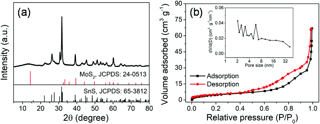 | ||
| Fig. 2 (a) XRD pattern and (b) N2 adsorption/desorption isotherms and pore size distribution curve (inset) of the MoS2@SnS heterostructure. | ||
X-ray photoelectron spectroscopy (XPS) measurements (Fig. 3) were performed to further investigate the chemical composition and surface electronic states of the MoS2@SnS heterostructures. The full XPS survey scan spectrum (Fig. S2, ESI†) verifies the presence of Sn, O, N, C, Mo, and S elements in the composite sample. The existence of N and C elements can be ascribed to the carbonization of trace PVP residue during heat treatment process. The carbon shell creates abundant extrinsic defects, which can improve the overall conductivity and enhance electrochemical performance of the MoS2@SnS heterostructure. The existence of O can be attributed to the adsorbed oxygen species on the sample surface. The high-resolution XPS spectrum of Mo 3d (Fig. 3a) shows four peaks located at ∼231.3, ∼228.0, ∼234.9 and ∼225.2 eV. The former two peaks correspond to Mo 3d3/2 and Mo 3d5/2 of Mo4+ in MoS2. The small peak at ∼234.9 eV is ascribed to the presence of a small amount of Mo6+ of MoO3 due to surface oxidation.38 The peak at ∼225.2 eV originates from the S 2s component in the MoS2@SnS composites. The high-resolution XPS spectrum of the Sn 3d core level (Fig. 3b) displays two main peaks at ∼494.3 and ∼485.9 eV corresponding to Sn 3d3/2 and Sn 3d5/2 of Sn2+ in SnS, respectively.27 The high-resolution S 2p spectrum (Fig. 3c) can be deconvoluted into two peaks at ∼161.9 and ∼160.7 eV, which can be assigned to S 2p1/2 and S 2p3/2 of S2− in MoS2@SnS, respectively.39 The high-resolution N 1s spectrum (Fig. 3d) suggests the presence of pyridinic N (398.5 eV) and pyrrolic N (400.2 eV) components in the MoS2@SnS heterostructure.
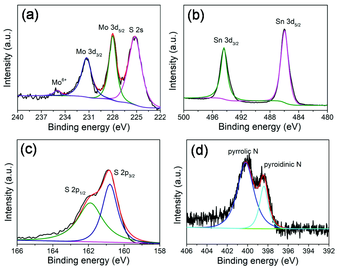 | ||
| Fig. 3 High-resolution XPS spectra of the MoS2@SnS heterostructure. (a) Mo 3d; (b) Sn 3d; (c) S 2p; and (d) N 1s spectra. | ||
The structure and morphology of the MoS2@SnS heterostructure were characterized by scanning electron microscopy (SEM), transmission electron microscopy (TEM), and high-resolution TEM (HRTEM). The SEM image (Fig. 4a) shows that the as-prepared MoG nanospheres have a diameter of ∼700 nm and a smooth surface. After the sulfuration process, the MoS2 nanospheres possess similar particle shapes but a rough surface (Fig. S3a†). The SEM images (Fig. 4b and c) of the MoS2@SnS heterostructure reveal the formation of a walnut-like heterostructure after decoration of SnS nanocrystals on MoS2 nanospheres during the hydrothermal process. The coating of SnS nanocrystals not only increases the contact area between the active materials and electrolyte but also buffers the volume variation to maintain the electrode integrity during charge/discharge. The TEM micrograph in Fig. 4d further discloses that the MoS2@SnS heterostructure has a diameter of ∼800 nm and a shell thickness of ∼50 nm. Fig. 4e and its inset show the HRTEM image of the edge of an individual MoS2@SnS nanosphere and the corresponding fast Fourier transform (FFT) pattern. In Fig. 4e, an ultrathin amorphous carbon layer can be observed as indicated by the white arrow at the margin of MoS2@SnS, which is consistent with the XPS result. The interplanar distance of 0.32 nm is in good agreement with the d-spacing of the (210) plane of orthorhombic SnS. The results confirmed the decoration of SnS nanocrystals on MoS2 nanospheres, leading to the formation of a hierarchical core–shell heterostructure. In contrast, the pure SnS sample is composed of nanosheet-constructed microflowers (Fig. S3b†). The energy-dispersive X-ray spectroscopy (EDS) mapping analysis of a single MoS2@SnS sphere shown in Fig. 4f–i further demonstrates the uniform distribution of Sn, Mo, S and N elements in the MoS2@SnS composite. The EDS mapping result suggests that the uniform coating of SnS on MoS2 helps to form a heterostructure.40
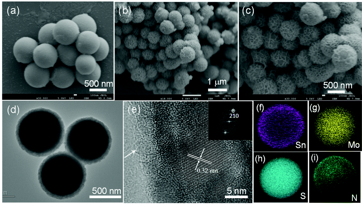 | ||
| Fig. 4 (a) SEM image of the MoG nanospheres; (b and c) SEM images of the MoS2@SnS heterostructures with different magnifications; (d) TEM image of the MoS2@SnS heterostructures; (e) HRTEM image of the MoS2@SnS heterostructures with the corresponding fast Fourier transform (FFT) pattern (inset); EDS elemental mapping of (f) Sn, (g) Mo, (h) S and (i) N elements in the MoS2@SnS composite. | ||
The electrochemical properties of the MoS2@SnS heterostructure were evaluated by cyclic voltammetry (CV) and galvanostatic charge/discharge tests. The CV curves of the MoS2@SnS electrode for the first three cycles at a scan rate of 0.1 mV s−1 in the potential range of 0.01–3 V (vs. Na+/Na) are shown in Fig. 5a. During the initial cathodic scanning process, a shoulder at ca. 0.9–1.2 V corresponds to the conversion reaction of SnS to Sn and Na2S24,26 as well as intercalation of Na into the MoS2 interlayer.41 The peak centered at ∼0.63 V can be ascribed to the alloying reaction of Sn and Na and conversion of MoS2 into Mo and Na2S as well as the formation of a solid electrolyte interface (SEI) film.42 Another peak appearing at ∼0.03 V suggests a multistep alloying reaction process of NaxSn and Na-ion storage at the Mo/Na2S interface.43 The formation of NaxSn alloys can effectively relieve the huge volume change during the multistep alloying reactions and thus improve the cycling stability. During charge, the peak at 0.2 V corresponds to the dealloying reaction of NaxSn into Na and Sn. Another peak centered at ∼1.16 V indicates the reverse conversion of Sn and Na2S into SnS, while the peak at ∼2.48 V (which shifts to ∼2.2 V and becomes broad in the 2nd/3rd cycle) is caused by the reverse conversion of Mo and Na2S into the MoS2 phase.44 The potential-dependent redox reactions involved in the whole charge/discharge processes can be summarized as follows:
| SnS + 2Na+ + 2e− → Sn + Na2S; |
| Sn + Na+ + xe− → NaxSn; |
| MoS2 + xNa+ + xe− → NaxMoS2; |
| NaxMoS2 + (4 − x)Na+ + (4 − x)e− ↔ Mo + 2Na2S. |
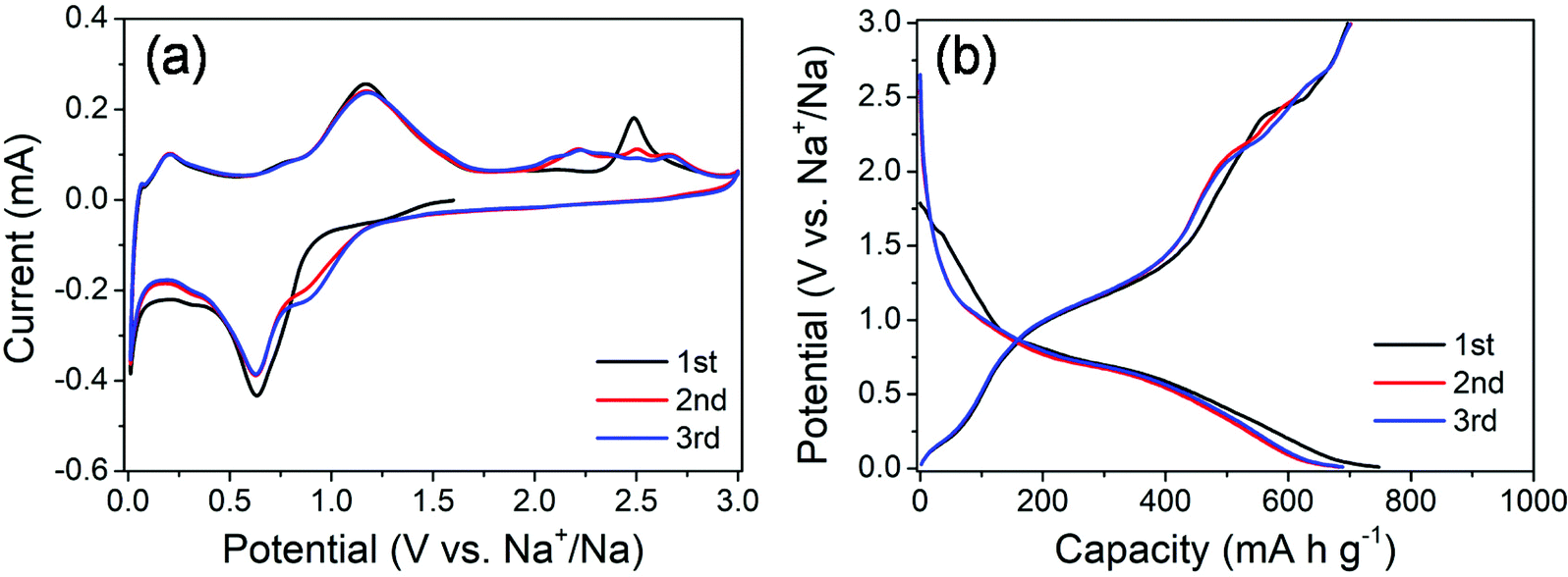 | ||
| Fig. 5 (a) CV curves of the MoS2@SnS heterostructure at a scan rate of 0.1 mV s−1 and (b) galvanostatic charge/discharge profiles of the MoS2@SnS heterostructure at a current density of 0.1 A g−1. | ||
The CV curves almost overlap in the subsequent cycles, indicating the formation of a stable SEI layer and high reversibility of electrochemical reactions in the MoS2@SnS electrode.
The galvanostatic charge/discharge profiles of MoS2@SnS at a current density of 0.1 A g−1 for the first three cycles are shown in Fig. 5b. The MoS2@SnS heterostructure delivers an initial discharge capacity of ∼747 mA h g−1 and a charge capacity of ∼697 mA h g−1, with a high initial coulombic efficiency (CE) of ∼93.3%. Such a high CE could be ascribed to the formation of a uniform and stable SEI layer at the surface of SnS, resulting from the strong interface synergistic effect of the MoS2 and SnS heterointerface for improved electrochemical activity.36 From the second cycle, the discharge and charge curves overlap well and no obvious capacity loss can be observed, revealing the good capacity retention and cyclability of the MoS2@SnS electrode.
The rate capability of the SnS microflowers, MoS2 nanospheres, and MoS2@SnS heterostructure is shown in Fig. 6a. The MoS2@SnS heterostructure electrode exhibits a high capacity of ∼662 mA h g−1 at 0.1 A g−1. As the current densities increase to 0.2, 0.5, 1.0 and 2.0 A g−1, the MoS2@SnS electrode can maintain reversible capacities of ∼614, 600, 596 and ∼586 mA h g−1, respectively. Even when the cycling current density increases to 5 A g−1, the MoS2@SnS electrode can still maintain a reversible capacity of ∼556 mA h g−1. After switching the current density back to 0.2 A g−1, the MoS2@SnS electrode can maintain a reversible capacity of ∼654 mA h g−1 again, indicating its good capacity reversibility, which makes it suitable as an anode material for SIBs. In comparison, the pure MoS2 nanosphere electrode exhibits an inferior sodium-ion storage property with capacities of ∼476, ∼418, ∼359, ∼317, ∼260, and ∼160 mA h g−1 at 0.1, 0.2, 0.5, 1.0, 2.0, and 5.0 A g−1, respectively. The SnS microflower electrode manifests an even lower rate capability under the same test conditions. The remarkable rate capability of the MoS2@SnS heterostructure can originate from the synergetic enhancement of electronic conductivity and sodium-ion transport kinetics, benefiting from the internal electric field at the heterointerfaces.34 The long-term cycling stability of the SnS microflowers, MoS2 nanospheres and MoS2@SnS heterostructures was further evaluated at 1.0 A g−1 as shown in Fig. 6b. The MoS2@SnS heterostructure displays a high and stable reversible capacity of ∼566 mA h g−1 after 500 cycles, implying excellent cycling stability. In contrast, the MoS2 nanospheres deliver a reversible capacity of ∼295 mA h g−1 after 500 cycles. Meanwhile, the SnS microflowers show a lower reversible capacity of ∼198 mA h g−1 after 300 cycles. These results further demonstrate the high sodium-ion storage capability and superior cycling stability of MoS2@SnS heterostructure anode materials for SIBs. To clarify the relationship between the architecture and electrochemical performance, the morphology of the MoS2@SnS heterostructures upon cycling was examined. The SEM images of the MoS2@SnS heterostructure after testing at 1 A g−1 for 100 cycles are shown in Fig. S4.† It can be seen that the original morphology of the MoS2@SnS heterostructure has been well preserved during the cycling process. Table S1† compares the sodium-ion storage properties of the MoS2@SnS heterostructure electrode with some transition-metal sulphides reported in the recent literature, demonstrating its better electrochemical performance.
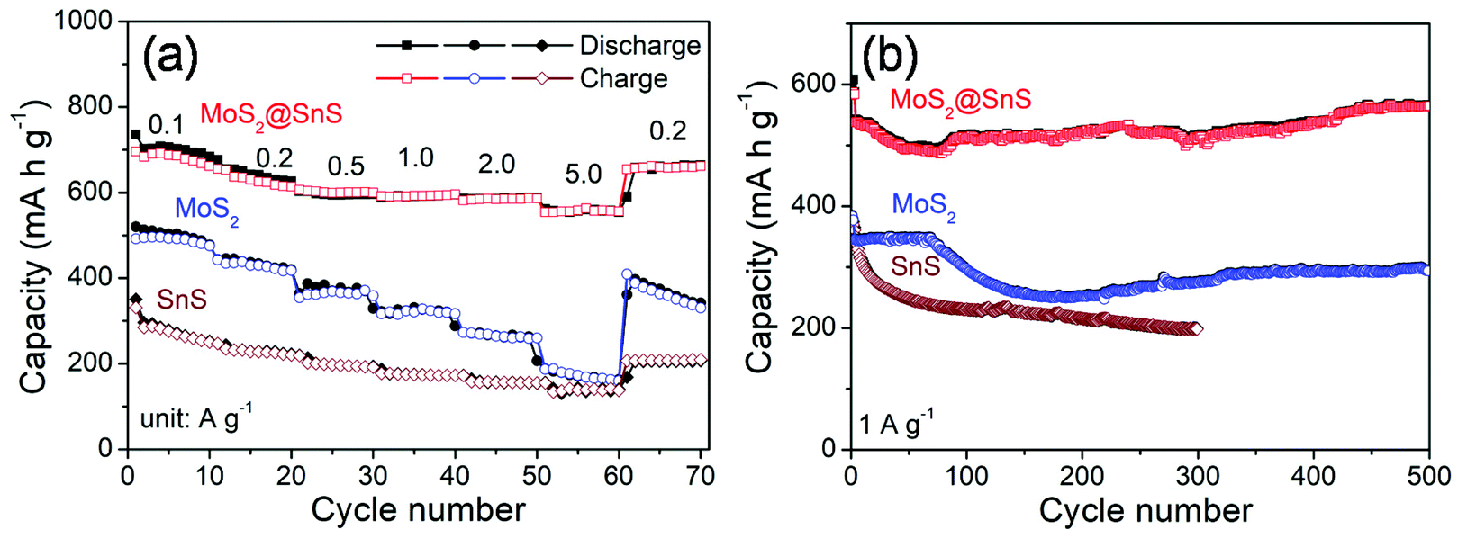 | ||
| Fig. 6 (a) Rate capability and (b) cycling stability of the SnS microflowers, MoS2 nanospheres and MoS2@SnS heterostructures at the indicated densities. | ||
The electrode reaction kinetics were studied via electrochemical impedance spectroscopy (EIS) before cycling. The Nyquist plots are composed of a depressed semicircle in the high-to-medium frequency region and an inclined line in the low frequency region (Fig. S5†). The depressed semicircle in the high-to-medium frequency region of the Nyquist plots corresponds to the SEI layer impedance (RSEI) and charge transfer impedance (Rct) between the electrode/electrolyte interface, and the sloping line at low frequency is related to Na+ diffusion in the solid phase.45,46 From the Nyquist plots, the MoS2@SnS heterostructure displays a smaller semicircle diameter, suggesting improved electrolyte/electrode interfacial characteristics after the formation of the MoS2@SnS core/shell heterojunction. The calculated interfacial impedances (Rint = RSEI + Rct) of the SnS microflowers, MoS2 nanospheres, and MoS2@SnS heterostructure are ∼106.9, ∼93.4 and ∼55.2 Ω, respectively. The reduced interface impedances can be attributed to enhanced electronic conductivity and sodium-ion transportation in the MoS2@SnS heterostructure. Moreover, EIS measurement of the MoS2@SnS heterostructure electrode after testing at 0.1 A g−1 for 100 cycles was carried out and the Nyquist plot is shown in Fig. S6†. Compared with the fresh one, a smaller, high-frequency semicircle is noted after cycling, demonstrating stable Na-ion storage capability during cycling.
In order to further investigate the origin of reaction kinetics, the CV curves of the MoS2@SnS heterostructure at various scan rates were recorded between 0.01 and 3 V (vs. Na+/Na), as shown in Fig. 7. The shapes of the CV curves are well preserved and a slightly positive shift for the anodic peaks and a negative shift for the cathodic peaks can be observed in Fig. 7a with increasing scan rates owing to polarization during the sodiation/desodiation process.47 The degree of the capacitive effect can be qualitatively analysed according to the relationship between the peak current (i) and scan rate (v) from the CV curves: i = avb, where i is the peak current, v stands for the scan rate, and a and b are both adjustable parameters. The value of b is between 0.5 and 1.0, which is determined by the slope of the log(i) vs. log(v) plot. It is well known that the electrochemical behavior is dominated by a surface capacitive process when b is close to 1.0, whereas for a diffusion-controlled process, b approaches 0.5. In the current experiment, the adjustable b values for peak 1, peak 2, and peak 3 are ∼0.84, ∼0.87, and ∼0.89, respectively, as shown in Fig. 7b, indicating more significant capacitive storage kinetics of the MoS2@SnS heterostructure.
 | ||
| Fig. 7 (a) CV curves at various scan rates ranging from 0.1 to 2.0 mV s−1; (b) plots of log(i) vs. log(v) at the sharp cathodic/anodic peak pair (peak current: i, scanning rate: v); (c) capacity contributions at different scan rates; and (d) capacitive charge storage contribution at a scan rate of 1.0 mV s−1. The estimated pseudocapacitance contribution is shown in the blue region. | ||
The contribution from the pseudocapacitive effects (both surface pseudocapacitive and double layer capacitance) and diffusion-controlled process to the current response can be calculated based on the following equation:48
| I(V) = k1v + k2v1/2 | (1) |
| I(V)/v1/2 = k1v1/2 + k2 | (2) |
The values of k1 (slope) and k2 (intercept) from the straight lines can be calculated by plotting I(V)/v1/2vs. v1/2 at different potentials. The percentage of the capacitive contribution at different scanning speeds can be calculated, as shown in Fig. 7c, demonstrating the percentages of the capacitive contribution can be improved with the increase of the scan rate, which may account for the high rate capability and superior cycling stability of Na+ storage in the designed MoS2@SnS heterostructure. Fig. 7d shows the typical voltage profile for the pseudocapacitive contribution (blue shaded region) in comparison with the whole area (black line). A large part of the pseudocapacitive contribution of ∼67.6% was achieved at a scan rate of 1 mV s−1, indicating favorable charge transfer kinetics of the MoS2@SnS heterostructure. Therefore, a large portion of the stored charge stems from the pseudocapacitive effect, which is in good agreement with the calculated b value.
More mechanistic insights are further gained from first-principles density functional theory (DFT) calculations. Fig. 8a shows the structure of MoS2@SnS after geometry optimization. From the charge difference contour plot, the red and green colors denote the electron gain and loss regions, respectively, indicating the charge redistribution at the MoS2@SnS interface and formation of the heterostructure. The optimized geometry structures of MoS2, SnS and MoS2@SnS heterostructure after intercalation of one Na are shown in Fig. 8b–d. The corresponding binding energies (Eb) are calculated to be ca. −2.25, −1.05 and −2.82 eV for MoS2, SnS and MoS2@SnS, respectively. The computational results indicate that Na insertion in all three structures is feasible and the intercalation in MoS2@SnS is more favored in energy. During Na insertion, the Na can donate most of its electrons to the MoS2@SnS framework as revealed by the charge difference plot.
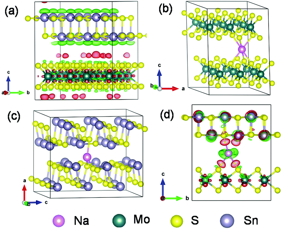 | ||
| Fig. 8 (a) The MoS2@SnS heterostructure after geometry optimization and the optimized geometry structures of (b) MoS2, (c) SnS supercells and (d) MoS2@SnS heterostructure after insertion of one Na atom. The corresponding binding energies (Eb) of one Na atom in (b) MoS2, (c) SnS and (d) MoS2@SnS are calculated to be ca. −2.25, −1.05 and −2.82 eV, respectively. The red and green colors in the charge difference contour plots of (a) and (d) represent the charge accumulation and depletion regions, respectively. The isosurface levels are 3.5 × 10⁻⁴ e bohr−3 in (a) and 2 × 10⁻³ e bohr−3 in (d). | ||
Next, we investigated Na diffusion in the three structures. As shown in Fig. 9a, Na can readily diffuse in the MoS2 (001) planes with a relatively small energy barrier (∼0.39 eV) (Fig. 9d). For SnS, the diffusion of Na along the (100) plane experiences a much higher energy barrier (3.0 eV) (Fig. 9d), possibly due to the scattering of Sn–S chains in this plane. In contrast, the diffusion of Na within the interface of MoS2(001)/SnS(100) is the fastest with the smallest energy barrier (∼0.016 eV). The much enhanced Na diffusion behavior further suggests that the existence of a built-in electric field at the interface can considerably propel the electronic/ionic transport and charge transfer, thus boosting the rate capability.
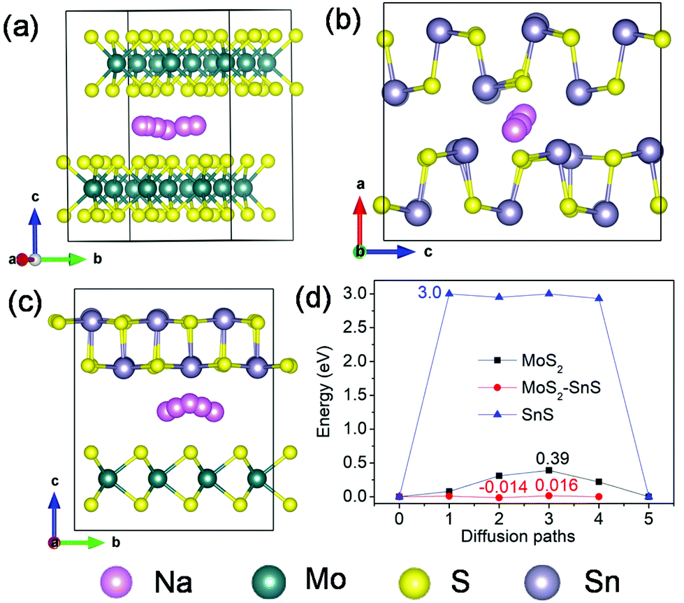 | ||
| Fig. 9 Possible diffusion pathways of Na in (a) MoS2, (b) SnS supercells and (c) MoS2@SnS heterostructure, and (d) the corresponding energy barriers for Na diffusion in MoS2, SnS and MoS2@SnS. | ||
Conclusions
In summary, a hierarchical walnut-like MoS2@SnS core–shell heterostructure has been designed and synthesized via a simple yet effective hydrothermal method. The heterostructure is comprised of MoS2 spheres wrapped by SnS nanocrystals. When evaluated as an anode material for SIBs, the MoS2@SnS heterostructure exhibited high capacity and initial coulombic efficiency, remarkable rate capability, and superior cycling stability, much superior to those of pure SnS microflowers and MoS2 nanospheres. The improved sodium-ion storage properties mainly stem from the increased charge transfer capability and ion diffusion kinetics due to the presence of an internal built-in electric field at the heterointerfaces during charge/discharge. It is believed that the unique core–shell architecture designed herein can pave the way for the development of novel heterojunction-based electrode materials for high-performance SIBs and other electrochemical energy storage and conversion devices.Experimental
Synthesis of the Mo-glycerate (MoG) precursor
Typically, 10 mL of H2O, 10 mL of glycerol, and 35 mL of isopropanol were mixed and stirred to form a homogeneous solution. Then, 150 mg of molybdenyl acetoacetonate was added into the resulting solution under magnetic stirring to obtain a transparent solution. The resultant solution was transferred to a Teflon-lined stainless steel autoclave (100 mL in volume) and maintained at 190 °C for 3 h. After cooling down to room temperature, the obtained product was centrifuged and washed with ethanol three times, and then dried at 60 °C for 12 h under vacuum.Synthesis of MoS2 nanospheres
Briefly, 100 mg of the as-prepared MoG solid spheres were dispersed in 25 mL of ethanol with the assistance of ultrasonication for 30 min to form a homogeneous suspension. Then, 10 mL of ethanol and 100 mg of Na2S were added into the above suspension and stirred for 10 min. The solution was transferred into a Teflon-lined stainless steel autoclave (100 mL in volume) and maintained at 200 °C for 10 h. The obtained MoS2 was centrifuged and washed with deionized water and ethanol three times, and then dried at 60 °C for 12 h under vacuum.Synthesis of SnS microflowers
500 mg of polyvinyl pyrrolidone (PVP, molecular weight of 40![[thin space (1/6-em)]](https://www.rsc.org/images/entities/char_2009.gif) 000) were dissolved in 50 mL of ethylene glycol followed by stirring and ultrasonication. Then, 225 mg of SnCl2 and 75 mg of thioacetamide were added into the solution and stirred for 10 min. Finally, the mixed solution was transferred into a sealed Teflon-lined stainless-steel autoclave (100 mL in volume) and maintained at 160 °C for 12 h. After cooling down, the product was centrifuged and washed with ethanol three times and then dried at 60 °C for 12 h under vacuum.
000) were dissolved in 50 mL of ethylene glycol followed by stirring and ultrasonication. Then, 225 mg of SnCl2 and 75 mg of thioacetamide were added into the solution and stirred for 10 min. Finally, the mixed solution was transferred into a sealed Teflon-lined stainless-steel autoclave (100 mL in volume) and maintained at 160 °C for 12 h. After cooling down, the product was centrifuged and washed with ethanol three times and then dried at 60 °C for 12 h under vacuum.
Synthesis of MoS2@SnS heterostructures
In the first step, 500 mg of PVP (molecular weight of 40000) and 50 mg of MoS2 nanospheres were successively added into 50 mL of ethylene glycol (EG) followed by stirring and ultrasonication to form a homogeneous solution. In the second step, 144 mg of SnCl2 and 288 mg of thioacetamide (TAA) were dissolved in 3.2 mL of ethylene glycol, respectively. Then, the two solutions were added into the above solution under stirring for 15 min. Subsequently, the mixed solution was transferred into a Teflon-lined stainless-steel autoclave (100 mL in volume) and kept at 160 °C for 12 h. After cooling down to room temperature, the MoS2@SnS heterostructures were centrifuged and washed with ethanol three times and then dried at 60 °C for 12 h under vacuum. Finally, the product was sintered at 400 °C for 2 h under a high-purity N2 atmosphere to increase the degree of crystallinity.
Characterization
The morphology and structure of the samples were characterized using a field-emission scanning electron microscope (FESEM; JEOL, Model JSM-7800F), a transmission electron microscope (TEM; Philips, CM20 operated at 200 kV), and a high-resolution TEM (HRTEM; CM200 FEG operated at 200 kV) with energy-dispersive X-ray spectroscopy (EDS). The X-ray diffraction (XRD) pattern was recorded on a Bruker D8 Advance X-Ray Diffractometer with Cu-Kα as the radiation source (λ = 0.154 nm). X-ray photoelectron spectroscopy (XPS) measurement was performed by using a VG ESCA-LAB 220i-XL UHV surface analysis system with a monochromatic Al Kα X-ray source (1486.6 eV). The Brunauer–Emmett–Teller (BET) method was used to evaluate the surface area and porous size distribution with N2 adsorption–desorption isotherms at 77 K.Electrochemical measurements
Electrochemical performances of the MoS2@SnS heterostructures were tested by assembling CR2032 coin-type cells in a high-purity argon-filled glovebox with sodium metal foils as counter and reference electrodes. The working electrode was fabricated by mixing the active materials (MoS2@SnS, MoS2, SnS), acetylene black, and binder (sodium alginate) in a weight ratio of 7:2:1 to form a uniform slurry in deionized water. The slurry was coated on copper foil and vacuum-dried at 70 °C for 12 h. The typical mass loading for the active materials was ∼1.5 mg cm−2. A solution of 1.25 M NaPF6 dissolved in ethyl methyl carbonate was used as the electrolyte. A glass fiber (Whatman, GF/D) was used as the separator. The galvanostatic discharge/charge measurements were performed on a LAND CT2001A test system at various current densities within a potential window of 0.01–3.0 V vs. Na+/Na. Cyclic voltammetry (CV) was carried out on a CHI 760E electrochemical workstation at a scanning rate of 0.1 mV s−1. Electrochemical impedance spectra (EIS) both before and after testing at 0.1 A g−1 for 100 cycles were measured on a ZAHNER-elektrik IM 6 electrochemical system in a frequency range from 100 kHz to 5 mHz. All the electrochemical tests were performed at room temperature.
Computational details
All the calculations were based on first-principles density functional theory (DFT) using plane-wave pseudopotentials with an exchange-correlation of Perdew–Burke–Ernzerhof (PBE) formation implemented in Vienna ab initio simulation package (VASP).50,51 An energy cutoff of 400 eV was used for plane wave expansion of the wavefunctions. The Brillouin zone was sampled with a 1 × 1 × 1 gamma-centered Monkhorst–Pack k-point mesh. The convergence criteria for the total energy and ionic forces were set to 10−5 eV and 0.03 eV Å−1, respectively. The binding energies (Eb) for Na intercalation in the respective structures were determined by Eb = Etotal − ENa − EMS, where Etotal, ENa, and EMS represent the calculated energies of the whole system, single Na atom in a vacuum, and host structure (MoS2, SnS or MoS2@SnS), respectively. The Na diffusion in the three host structures (MoS2, SnS and MoS2@SnS) was calculated via the climbing-image nudged elastic band (CI-NEB) method. During the calculations, van der Waals interactions (DFT-D3) were considered. The drawing of the calculated results was carried out using VESTA software.52Conflicts of interest
There are no conflicts to declare.Acknowledgements
The authors acknowledge the support by a grant from the National Natural Science Foundation of China Program (No. 51602111), the Xijiang R&D Team (X.W.), the Guangdong Provincial Grant (2017A010104013), the Guangdong Provincial Key Laboratory of Optical Information Materials and Technology (Grant No. 2017B030301007), and the Beijing Super Cloud Computing Center (BSCC) for providing HPC resources that have contributed to the DFT calculation results reported in this paper. URL: http://www.blsc.cn/.Notes and references
- Q. Zhang, E. Uchaker, S. L. Candelaria and G. Cao, Chem. Soc. Rev., 2013, 42, 3127–3171 RSC.
- G. Zhao, Y. Zhang, Z. Gao, H. Li, S. Liu, S. Cai, X. Yang, H. Guo and X. Sun, ACS Energy Lett., 2020, 5, 1022–1031 CrossRef CAS; W. Wang, Y. Guo, L. Liu, S. Wang, X. Yang and H. Guo, J. Power Sources, 2014, 245, 624–629 CrossRef; H. Guo, L. Liu, T. Li, W. Chen, J. Liu, Y. Guo and Y. Guo, Nanoscale, 2014, 6, 5491–5549 RSC; H. Guo, R. Mao, D. Tian, W. Wang, D. Zhao, X. Yang and S. Wang, J. Mater. Chem. A, 2013, 1, 3652–3658 RSC; Y. Cai, H. E. Wang, X. Zhao, F. Huang, C. Wang, Z. Deng, Y. Li, G. Z. Cao and B. L. Su, ACS Appl. Mater. Interfaces, 2017, 9, 10652–10663 CrossRef PubMed.
- X. C. Li, G. L. Guo, N. Qin, Z. Deng, Z. G. Lu, D. Shen, X. Zhao, Y. Li, B. L. Su and H. E. Wang, Nanoscale, 2018, 10, 15505–15512 RSC; H. E. Wang, K. L. Yin, X. Zhao, N. Qin, Y. Li, Z. Deng, L. C. Zheng, B. L. Su and Z. G. Lu, Chem. Commun., 2018, 54, 12250–12253 RSC; H. E. Wang, K. L. Yin, N. Qin, X. Zhao, F. J. Xia, Z. Y. Hu, G. L. Guo, G. Z. Cao and W. J. Zhang, J. Mater. Chem. A, 2019, 7, 10346010353 Search PubMed; H. E. Wang, X. C. Li, N. Qin, X. Zhao, H. Cheng, G. Z. Cao and W. J. Zhang, J. Mater. Chem. A, 2019, 7, 12068–12074 RSC.
- D. Kundu, E. Talaie, V. Duffort and L. F. Nazar, Angew. Chem., Int. Ed., 2015, 54, 3431–3448 CrossRef CAS PubMed.
- M. S. Islam and C. A. Fisher, Chem. Soc. Rev., 2014, 43, 185–204 RSC.
- N. Yabuuchi, K. Kubota, M. Dahbi and S. Komaba, Chem. Rev., 2014, 114, 11636–11682 CrossRef CAS PubMed.
- Y. Dong, M. Hu, Z. Zhang, J. A. Zapien, X. Wang, J. M. Lee and W. Zhang, ACS Appl. Nano Mater., 2019, 2, 1457–1465 CrossRef CAS.
- Z. Liu, X. Y. Yu, X. W. Lou and U. Paik, Energy Environ. Sci., 2016, 9, 2314–2318 RSC.
- H. Hou, X. Qiu, W. Wei, Y. Zhang and X. Ji, Adv. Energy Mater., 2017, 7, 1602898 CrossRef.
- Y. Zhao and A. Manthiram, Chem. Mater., 2015, 27, 3096–3101 CrossRef CAS.
- X. Zhou, L. Yu and X. W. D. Lou, Adv. Energy Mater., 2016, 6, 1600451 CrossRef CAS; Q. Y. Ren, N. Qin, B. Liu, Y. Yao, X. Zhao, Z. Deng, Y. Li, Y. C. Dong, D. Qian, B. L. Su, W. J. Zhang and H. E. Wang, J. Mater. Chem. A, 2020, 8, 3450–3458 RSC.
- Y. Zhao, L. P. Wang, M. T. Sougrati, Z. Feng, Y. Leconte, A. Fisher, M. Srinivasan and Z. Xu, Adv. Energy Mater., 2017, 7, 1601424 CrossRef.
- H. Liu, H. Guo, B. Liu, M. Liang, Z. Lv, K. R. Adair and X. Sun, Adv. Funct. Mater., 2018, 28, 1707480 CrossRef CAS; H. Liu, B. H. Liu, H. Guo, M. F. Liang, Y. H. Zhang, T. Borjigin, X. F. Yang, L. Wang and X. L. Sun, Nano Energy, 2018, 51, 639–648 CrossRef; X. Zhao, W. Cai, Y. Yang, X. D. Song, Z. Neale, H. E. Wang, J. H. Sui and G. Z. Cao, Nano Energy, 2018, 47, 224–234 CrossRef; L. Xu, P. Xiong, L. Zeng, Y. Fang, R. Liu, J. Liu, F. Luo, Q. Chen, M. Wei and Q. Qian, Nanoscale, 2019, 11, 16308–16316 RSC.
- W. Lv, J. Xiang, F. Wen, Z. Jia, R. Yang, B. Xu, D. Yu, J. He and Z. Liu, Electrochim. Acta, 2015, 153, 49–54 CrossRef CAS.
- H. Shu, F. Li, C. Hu, P. Liang, D. Cao and X. Chen, Nanoscale, 2016, 8, 2918–2926 RSC.
- N. S. Mikhaleva, M. A. Visotin, A. A. Kuzubov and Z. I. Popov, J. Phys. Chem. C, 2017, 121, 24179–24184 CrossRef CAS.
- S. H. Choi, Y. N. Ko, J.-K. Lee and Y. C. Kang, Adv. Funct. Mater., 2015, 25, 1780–1788 CrossRef CAS.
- Q. Pan, Q. Zhang, F. Zheng, Y. Liu, Y. Li, X. Ou, X. Xiong, C. Yang and M. Liu, ACS Nano, 2018, 12, 12578–12586 CrossRef CAS PubMed.
- Y. L. Bai, Y. S. Liu, C. Ma, K. X. Wang and J. S. Chen, ACS Nano, 2018, 12, 11503–11510 CrossRef CAS PubMed.
- S.-K. Park, S. H. Yu, S. Woo, J. Ha, J. Shin, Y. E. Sung and Y. Piao, CrystEngComm, 2012, 14, 8323 RSC.
- K. Chang and W. Chen, Chem. Commun., 2011, 47, 4252–4254 RSC.
- J. Pei, H. Geng, E. H. Ang, L. Zhang, X. Cao, J. Zheng and H. Gu, Nanoscale, 2018, 10, 17327–17334 RSC.
- C. Bommier and X. Ji, Isr. J. Chem., 2015, 55, 486–507 CrossRef CAS.
- X. Hu, J. Chen, G. Zeng, J. Jia, P. Cai, G. Chai and Z. Wen, J. Mater. Chem. A, 2017, 5, 23460–23470 RSC.
- P. He, Y. Fang, X. Y. Yu and X. W. D. Lou, Angew. Chem., Int. Ed., 2017, 56, 12202–12205 CrossRef CAS PubMed.
- T. Zhou, W. K. Pang, C. Zhang, J. Yang, Z. Chen, H. K. Liu and Z. Guo, ACS Nano, 2014, 8, 8323–8333 CrossRef CAS PubMed.
- P. Xue, N. Wang, Y. Wang, Y. Zhang, Y. Liu, B. Tang, Z. Bai and S. Dou, Carbon, 2018, 134, 222–231 CrossRef CAS.
- W. Wang, L. Shi, D. Lan and Q. Li, J. Power Sources, 2018, 377, 1–6 CrossRef CAS.
- Y. Wang, J. Xu, H. Wu, M. Xu, Z. Peng and G. Zheng, J. Mater. Chem., 2012, 22, 21923 RSC.
- L. Yin, S. Chai, J. Huang, X. Kong and L. Pan, Electrochim. Acta, 2017, 238, 168–177 CrossRef CAS.
- J. Wang, J. Liu, H. Yang, D. Chao, J. Yan, S. V. Savilov, J. Lin and Z. X. Shen, Nano Energy, 2016, 20, 1–10 CrossRef CAS.
- Y. Guo, J. Tang, H. Qian, Z. Wang and Y. Yamauchi, Chem. Mater., 2017, 29, 5566–5573 CrossRef CAS.
- T. Liu, Y. Zhao, L. Gao and J. Ni, Sci. Rep., 2015, 5, 9307 CrossRef CAS PubMed.
- X. Chang, T. Wang, P. Zhang, J. Zhang, A. Li and J. Gong, J. Am. Chem. Soc., 2015, 137, 8356–8359 CrossRef CAS PubMed.
- Y. Zheng, T. Zhou, C. Zhang, J. Mao, H. Liu and Z. Guo, Angew. Chem., Int. Ed., 2016, 55, 3408–3413 CrossRef CAS PubMed.
- X. Man, P. Liang, H. Shu, L. Zhang, D. Wang, D. Chao, Z. Liu, X. Du, H. Wan and H. Wang, J. Phys. Chem. C, 2018, 122, 24600–24608 CrossRef CAS.
- B. H. Baby and D. B. Mohan, Mater. Chem. Phys., 2017, 192, 317–329 CrossRef CAS.
- Y. Teng, H. Zhao, Z. Zhang, Z. Li, Q. Xia, Y. Zhang, L. Zhao, X. Du, Z. Du, P. Lv and K. Swierczek, ACS Nano, 2016, 10, 8526–8535 CrossRef CAS PubMed.
- I. Song, C. Park, M. Hong, J. Baik, H. J. Shin and H. C. Choi, Angew. Chem., Int. Ed., 2014, 53, 1266–1269 CrossRef CAS PubMed.
- H. E. Wang, X. Zhao, X. Li, Z. Wang, C. Liu, Z. Lu, W. Zhang and G. Cao, J. Mater. Chem. A, 2017, 5, 25056–25063 RSC.
- J. J. Wang, C. Luo, T. Gao, A. Langrock, A. C. Mignerey and C. S. Wang, Small, 2015, 11, 473–481 CrossRef CAS PubMed.
- S. H. Choi and Y. C. Kang, Nano Res., 2015, 8, 1595–1603 CrossRef CAS.
- Y. C. Lu, C. Ma, J. Alvarado, N. Dimov, Y. S. Meng and S. Okada, J. Mater. Chem. A, 2015, 3, 16971–16977 RSC.
- B. Chen, E. Liu, T. Cao, F. He, C. Shi, C. He, L. Ma, Q. Li, J. Li and N. Zhao, Nano Energy, 2017, 33, 247–256 CrossRef CAS.
- H. E. Wang, L. X. Zheng, C. P. Liu, Y. K. Liu, C. Y. Luan, H. Cheng, Y. Y. Li, L. Martinu, J. A. Zapien and I. Bello, J. Phys. Chem. C, 2011, 115, 10419–10425 CrossRef CAS.
- Y. Dong, S. Yang, Z. Zhang, J. M. Lee and J. A. Zapien, Nanoscale, 2018, 10, 3159–3165 RSC.
- Y. Dong, M. Hu, Z. Zhang, J. A. Zapien, X. Wang and J. M. Lee, Nanoscale, 2018, 10, 13343–13350 RSC.
- J. B. Cook, H. S. Kim, Y. Yan, J. S. Ko, S. Robbennolt, B. Dunn and S. H. Tolbert, Adv. Energy Mater., 2016, 6, 1501937 CrossRef.
- Z. Y. Zhang, S. Wu, J. Cheng and W. Zhang, Energy Storage Mater., 2018, 15, 65–74 CrossRef.
- J. P. Perdew, K. Burke and M. Ernzerhof, Phys. Rev. Lett., 1996, 77, 3865 CrossRef CAS PubMed.
- G. Kresse and D. Joubert, Phys. Rev. B: Condens. Matter Mater. Phys., 1999, 59, 1758 CrossRef CAS.
- K. Momma and F. Izumi, J. Appl. Crystallogr., 2011, 44, 1272–1276 CrossRef CAS.
Footnotes |
| † Electronic supplementary information (ESI) available. See DOI: 10.1039/d0nr02604b |
| ‡ These authors contributed to this work equally. |
| This journal is © The Royal Society of Chemistry 2020 |