
 Open Access Article
 This Open Access Article is licensed under a Creative Commons Attribution-Non Commercial 3.0 Unported Licence
Universal direct patterning of colloidal quantum dots by (extreme) ultraviolet and electron beam lithography†
Christian D.
Dieleman
 a,
Weiyi
Ding
a,
Lianjia
Wu
b,
Neha
Thakur
b,
Ivan
Bespalov
b,
Benjamin
Daiber
a,
Yasin
Ekinci
c,
Sonia
Castellanos
*b and
Bruno
Ehrler
*a
a,
Weiyi
Ding
a,
Lianjia
Wu
b,
Neha
Thakur
b,
Ivan
Bespalov
b,
Benjamin
Daiber
a,
Yasin
Ekinci
c,
Sonia
Castellanos
*b and
Bruno
Ehrler
*a
aAMOLF, Center for Nanophotonics, Science Park 104, 1098XG Amsterdam, The Netherlands. E-mail: B.Ehrler@amolf.nl
bAdvanced Research Center for Nanolithography, EUV Photoresists Group, Science Park 106, 1098 XG Amsterdam, The Netherlands. E-mail: S.Castellanos@arcnl.nl
cPaul Scherrer Institute, Laboratory of Micro and Nanotechnology, Forschungsstrasse 111, 5232 Villigen, Switzerland
First published on 18th May 2020
Abstract
Colloidal quantum dots have found many applications and patterning them on micro- and nanoscale would open a new dimension of tunability for the creation of smaller scale (flexible) electronics or nanophotonic structures. Here we present a simple, general, one-step top-down patterning technique for colloidal quantum dots by means of direct optical or electron beam lithography. We find that both photons and electrons can induce a solubility switch of both PbS and CdSe quantum dot films. The solubility switch can be ascribed to cross-linking of the organic ligands, which we observe from exposure with deep-UV photons (5.5 eV) to extreme-UV photons (91.9 eV), and low-energy (3–70 eV) as well as highly energetic electrons (50 keV). The required doses for patterning are relatively low and feature sizes can be as small as tens of nanometers. The luminescence properties as well as carrier lifetimes remain similar after patterning.
Introduction
Colloidal quantum dots (CQDs) have developed to be a high-performance and reliable platform for numerous applications ranging from photovoltaics,1,2 to LEDs,3,4 single photon sources,5,6 transistors7,8 and many more.9,10 This class of nanocrystals is extremely versatile due to their tunable properties in terms of size, composition and surface chemistry, which in turn influence important characteristics like bandgap, absorption and emission wavelengths, photoluminescence quantum yield, charge transport, processability, colloidal stability and film formation properties.11 Extending the unique tunability of these nanocrystals by patterning them on the micro- or nanoscale can lead to entirely new applications, for instance small LEDs for high resolution (flexible) displays12 or waveguiding structures that support directional emission.13 Ultimately, nanostructuring on the scale of the wavelength of light can lead to collective effects such as resonances, allowing for enhanced emission and absorption of metasurfaces.14 Manufacturing of these structures requires multiple intricate processing steps, like stamping,12 template stripping13 or multistep lithography with lift-off.15Typically, nanostructures for large-scale applications are written by (deep) ultraviolet lithography (λ = 193–365 nm, DUVL). The resolution of DUVL is limited by its wavelength and sub-20 nm features can only be reached with complex multi-step exposures. This complexity pushes the industry to introduce a new technique based on extreme UV lithography (λ = 13.5 nm, EUVL), which will likely become the standard in large scale lithography manufacturing over the next years. Photolithography processes rely on masks to write the nanostructures onto a substrate covered with photoresist. The illumination light induces a solubility change of the resist, which allows for subsequent dissolution of either the illuminated (positive tone) or unexposed (negative tone) areas. Maskless e-beam lithography (EBL) on the other hand is used for smaller structures, lab-scale prototyping and experiments, as well as photomask fabrication. The e-beam directly induces the chemical changes in the resist material, similarly leading to a solubility contrast between exposed and unexposed areas.
Previous work has been carried out on patterning of colloidal quantum dots. Wang et al. exploited the degradation of 1,2,3,4-thiatriazole-5-thiolate capping ligands. These are soluble in polar solvents, and become insoluble thiocyanate ligands, by UV-radiation (λ = 254 nm).16 This approach with other light-sensitive ligands was later expanded to include blue-light lithography (λ = 405, 450 nm) as well.17 Palazon et al. used X-rays from an XPS source (λ = 0.83 nm, 1486.6 eV) to pattern nanocrystals directly by cross-linking the ligands.18 Highly energetic e-beam has also been explored for direct patterning of metallic nanoparticles19,20 and more recently for semiconductor nanocrystals (30 keV, 100 keV),21,22 and other more energetic sources summarized in an overview by Palazon et al.23
Here we show a general, single-step, resistless method that allows direct pattering of two different semiconductor quantum dots (CdSe, PbS) with either low- or high-energy photons (5.5 eV or 91.9 eV; DUV & EUV) or low- to high-energy electron beams (3 eV–50 keV). We find that the quantum dot ligands cross-link upon exposure, making the exposed areas insoluble. This technique allows patterning of nanostructures down to tens of nanometers. The photoluminescence efficiency remains almost constant upon patterning, making the pattering technique suitable for optical applications.
Results and discussion
We synthesized two types of colloidal quantum dots from CdSe and PbS. These materials have been used in e.g. solar cells and for light emitting applications. Both materials were capped with their native ligands oleic acid, a mono-unsaturated, long (C18) carboxylic acid. We then deposited these CQDs by spin coating thin films onto silicon substrates and exposed them to five different exposure sources; three UV light sources in the form of near UV light (λ = 365 nm, 3.4 eV) from a MA BA 6 Mask aligner, more energetic light from a YAG DUV laser (λ = 225 nm, 5.5 eV) and EUV light (λ = 13.5 nm, 91.9 eV) from a synchrotron (Swiss Light Source) as well as two electron beam sources with either low energy electrons (0–70 eV) in a Low Energy Electron Microscope (LEEM, SPECS P90), or high-energy electrons (50 kV) in a commercial EBL system (Raith Voyager). To pattern the CQDs by EUV lithography we used open frame exposure for large areas (0.5 × 0.5 mm2), or diffractive transmission optics to write either lines or pillars using interference lithography. The size of the features was varied by changing the grating period. After exposure, the samples were developed by dipping into toluene or hexane for 10 seconds.By exposing the CQDs to the UV light or electron beam irradiation, chemical reactions are induced. These reactions can include cross-linking between the quantum dot ligands, upon which exposed areas become insoluble in the developer. This solubility change allows for contrast between the exposed and un-exposed areas and the formation of nanostructures of nanocrystals (Fig. 1a). Upon exposure with EUV photons, the high energy of the photons induces ionization events in the absorbing atom, leading to the creation of photoelectrons, holes and reactive radicals.24 These electrons typically still have a relatively high energy of around 80 eV (ref. 25) and can scatter inelastically with other electrons, losing energy along the way. The energy transfer from the photoelectron to the surroundings can promote excitations and even ionization events. Typical chemical bonds in organic materials, like the C–C or C–H bond have a bond strength of 3.6 eV and 4.4 eV respectively.26 Yet even electrons with energy much lower than this bond strength can induce chemical change in the material by means of dissociative electron attachment, where electrons are trapped by a molecule in an antibonding orbital.24,27 This process results in bond cleavage and subsequently in the generation of reactive species like radicals which can react with double bonds and induce the formation of new bonds, leading to the carbon chains cross-linking.28,29 As the absorption of one EUV photon can lead to a multiple of lower-energy photoelectrons, EUV radiation can have an inherent chemical amplification, possibly requiring lower exposure doses.
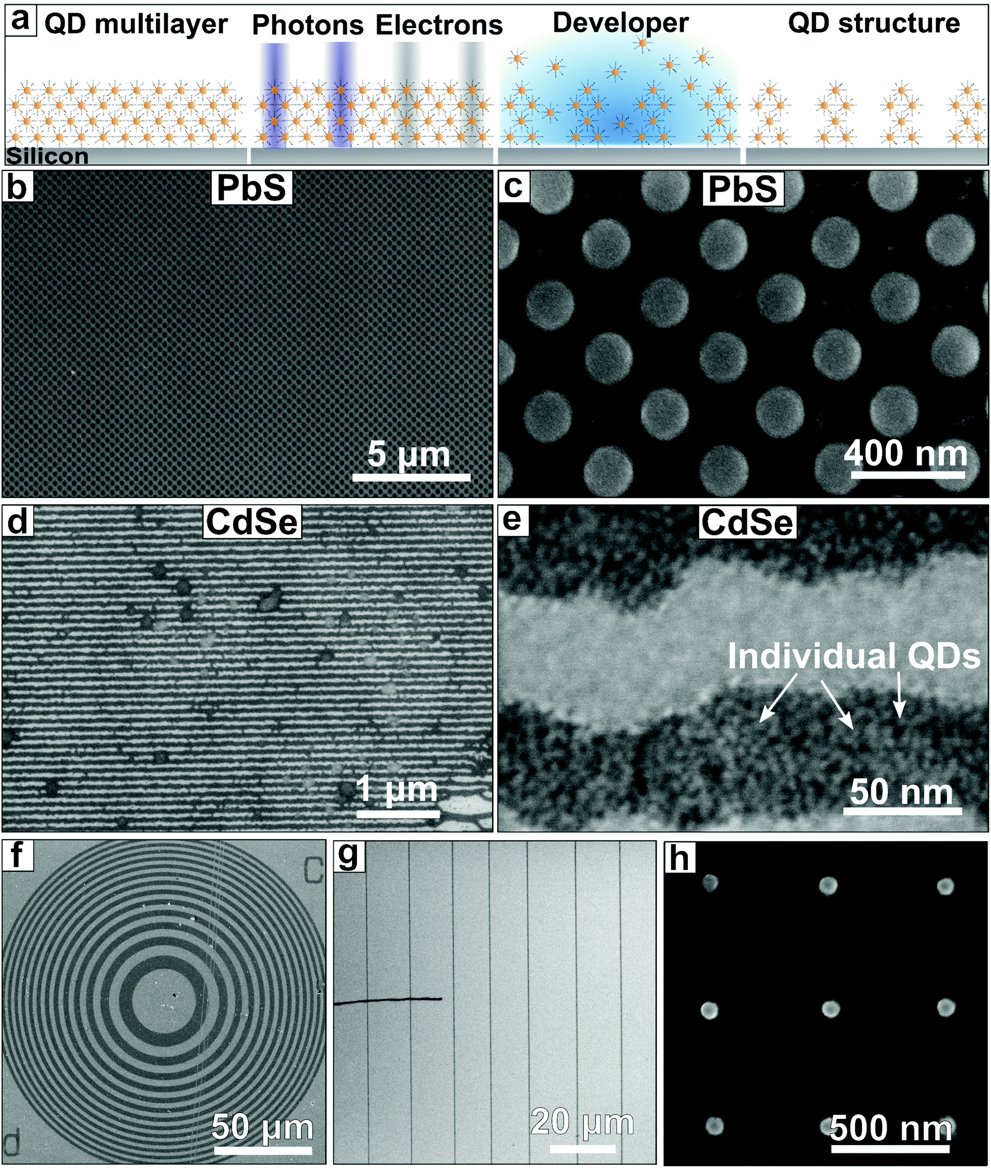 | ||
| Fig. 1 (a) Direct quantum dot patterning with different irradiation sources. Colloidal quantum dots are spin coated onto silicon substrates to form thin films. After irradiation with photons or electrons with different energies, the particles cluster together through cross-linking of their organic shells. After submersion in an apolar developer, the irradiated structures remain on the substrates, while non-irradiated quantum dots dissolve. Images (b–h) are SEM images. (b) Large field of patterned PbS pillars (180 nm diameter, 400 nm pitch) after EUV-exposure (140 mJ cm−2) and development. Very few defects are present. (c) Close up of patterned PbS pillars. (d) Large-scale field of EUV-patterned CdSe lines. Exposure dose (55 mJ cm−2). (e) Close up of CdSe lines. The individual quantum dots can easily be identified. (f) Larger, circular structure of CdSe QDs written with e-beam lithography (100 μC cm−2). (g) Thin (∼100 nm) lines of CdSe written with e-beam (100 μC cm−2). (h) Pillars of CdSe quantum dots with a diameter around 65 nm written with 100 μC cm−2 e-beam dose. | ||
By e-beam exposure, high-energy electrons have a similar effect as high-energy photons: ionization and generation of an electron cascade that leads to similar reactions. Next to the photoelectrons created by ionization of the resist molecules, secondary electrons emitted from the substrate also play a role, as the mean free path of electrons from a high-energy keV electron beam is longer (∼10s of nm) than that of photoelectrons emitted after EUV- photon absorption, which is expected to be in the 1 nm range.24 Based on the potential cross-linking chemistry of oleic acid ligands, we anticipated that exposure to radiation could transform the material into a cohesive network of nanocrystals which is insoluble in the developing solvents, even though the unexposed quantum dots are colloidally stable in the same solvents for months.
After spin coating thin films of PbS and CdSe we exposed them to EUV and e-beam radiation. Fig. 1b–e shows pillars written in PbS CQD films by EUV (180 nm pillar diameter, 400 nm pitch, 140 mJ cm−2, Fig. 1b and c) and line/space patterns written by EUV in CdSe CQD films (50 nm line width, 100 nm pitch, 55 mJ cm−2, Fig. 1d and e). More examples can be found in the ESI (section S1†). A clear contrast is observed after development, as the CQDs remain in the areas where the sample was exposed to EUV light. The pattern is visible and uniform over large areas of several μm2. The development is rapid, with almost no CQDs left in the unexposed areas after 10 s of immersion in the developer. Fig. 1f–h show some typical structures created by e-beam lithography. In this case we use a 50 keV electron beam (100 μC cm−2), which leads to a large number of secondary electrons with a broad energy distribution. As in the case of EUV exposure, we find that the e-beam exposed areas remain on the substrate upon development. The structures are well-resolved, rendering the smallest structures down to around 60 nm, which corresponds to a diameter of ∼10 quantum dots clustering together. From these observations, one can conclude that it is possible to pattern these materials well below the diffraction limit of DUV lithography in a one-step e-beam exposure.
To identify the chemical changes leading to the clustering of the nanocrystals and their solubility switch, we investigated samples exposed to different doses of EUV light (0 to 340 mJ cm−2) with Fourier Transform Infrared Spectroscopy (FTIR). The QD ligand, oleic acid, is a relatively simple molecule, an 18-carbon-atom long mono-unsaturated molecule, with a carboxylic end group. The most prominent features in the FTIR spectra are the features between 2800 and 3100 cm−1, between 1300 and 1600 cm−1 and around 1100 cm−1 (see Fig. 2).
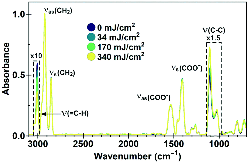 | ||
| Fig. 2 FTIR spectra of EUV exposed PbS films. Vibrational features are indicated. Parts of the spectra in the dashed boxes are magnified for clarity. The C–H stretching around the double bond decreases and the C–C stretching increases after exposure, indicating cross-linking of the carbon chains. The carboxylic anchoring group is unaffected. Spectra are normalized with respect to the CH2 stretches. | ||
The absence of an absorption peak around 1700 cm−1 indicates the absence of protonated –COOH end groups, which would reveal the presence of unreacted excess of oleic acid in the sample before exposure, or the formation of free ligands upon exposure. The peaks between 1300 and 1600 cm−1 are related to the symmetric and asymmetric stretching modes of deprotonated carboxylate COO− as bound to inorganic nanoparticles and quantum dots.30–32 The absorption between 1300–1700 cm−1 does not change as function of dose, and we therefore conclude that the binding of the ligands to the crystal surface remains unaffected, which is important for maintaining a passivated QD surface. The high wavenumber region, around 2925 cm−1, corresponds to stretching modes of CH2 (2850 cm−1), CH3 (2950 cm−1)32,33 and the CH bending of the C![[double bond, length as m-dash]](https://www.rsc.org/images/entities/char_e001.gif) CH bonds (3005 cm−1).34 We observe a systematic decrease and broadening of the peak at 3005 cm−1, which corresponds to a reduction in the number of double bonds when higher doses of EUV are interacting with the sample. The often used, but generally weak feature for CC around 1650–1640 cm−1 was on the level of the noise and therefore not used in this analysis. CC features below 1000 cm−1 were difficult to separate from –CH modes that are present due to different possible configurations of the oleic acid molecule, as well as influenced by the background signal of the silicon substrates and therefore not used. Finally, we observe an increase in the peak around 1105 cm−1, commonly attributed to C–C–H stretching in metal oleate molecules.33 An increase in this peak upon exposure can be rationalized by formation of new C–C–H bonds. Taken together, these changes demonstrate the cross-linking of the ligands at the position of the double bond in the carboxylic acid molecule. The cross-linking then turns the nanocrystal film into an insoluble, interlinked solid. Presumably, to form a coupled network, only a small number of cross-links per quantum dot are necessary to switch the solubility. The peak at 3005 cm−1 does not disappear even at the highest dose, meaning that many ligands remain unchanged.
CH bonds (3005 cm−1).34 We observe a systematic decrease and broadening of the peak at 3005 cm−1, which corresponds to a reduction in the number of double bonds when higher doses of EUV are interacting with the sample. The often used, but generally weak feature for CC around 1650–1640 cm−1 was on the level of the noise and therefore not used in this analysis. CC features below 1000 cm−1 were difficult to separate from –CH modes that are present due to different possible configurations of the oleic acid molecule, as well as influenced by the background signal of the silicon substrates and therefore not used. Finally, we observe an increase in the peak around 1105 cm−1, commonly attributed to C–C–H stretching in metal oleate molecules.33 An increase in this peak upon exposure can be rationalized by formation of new C–C–H bonds. Taken together, these changes demonstrate the cross-linking of the ligands at the position of the double bond in the carboxylic acid molecule. The cross-linking then turns the nanocrystal film into an insoluble, interlinked solid. Presumably, to form a coupled network, only a small number of cross-links per quantum dot are necessary to switch the solubility. The peak at 3005 cm−1 does not disappear even at the highest dose, meaning that many ligands remain unchanged.
Further evidence of such cross-linking was found by measuring the height profile of an EUV exposed PbS film with Atomic Force Microscopy (AFM) mapping shown in the ESI (section S2†). The film shows virtually no reduction in thickness at the edge of an exposed area before development. This result is consistent with the observation that only a fraction of the ligands cross-link the QDs and rules out major loss of ligands by outgassing. The phase map in the AFM, however, shows a high contrast between exposed and unexposed areas. The shift of phase angle from 3° to 25° can be correlated to a change in the visco-elastic properties of the material, where higher phase-shifts are related to a stiffer material due to stronger repulsion of the AFM tip, even though this change is difficult to quantify.35 A stiffer material is consistent with cross-links of the organic ligands into a denser network.
In order to determine the optimal dose for writing nanostructures with EUV, we write the PbS pillars at a range of intensities and measured their topology with AFM (Fig. 3). We find that even at low exposures (40 ± 6 mJ cm−2) we obtain the regular pattern after development, yet very thin. The features are on the order of 5–10 nm high. Presumably, the low number of photons only cross-links a fraction of the particles, slowing down the dissolution rate.36 When increasing the dose, the features become thicker and more clearly resolved, with sharper contrast between lines and spaces and a more reproducible shape. At 80–120 ± 15 mJ cm−2 we find well-resolved features and the thickness saturates at 40 nm, which is as thick as the original film. We find that the maximum film thickness needs to be on the same order as the desired feature size, as the maximum aspect ratio (height/width) of features is a little over 1. The relatively low dose required to write structures with EUV is particularly desirable because in commercial applications, which require an even lower dose of 20–30 mJ cm−2, the EUV photons are produced from tin-droplet plasma, which is expensive. At higher doses the features remain easily distinguishable, but the feature size keeps increasing with dose, indicating overexposure. Overexposure emerges when the number of photons necessary for a solubility switch is surpassed outside of the intended region. As the features are written with interference lithography, the light pattern consists of sinusoidal intensity patterns with a certain slope between minima and maxima. This leads to broadening of the written features when the dose is increased beyond the intensity threshold, as explained in more detail in the ESI (section S3†).
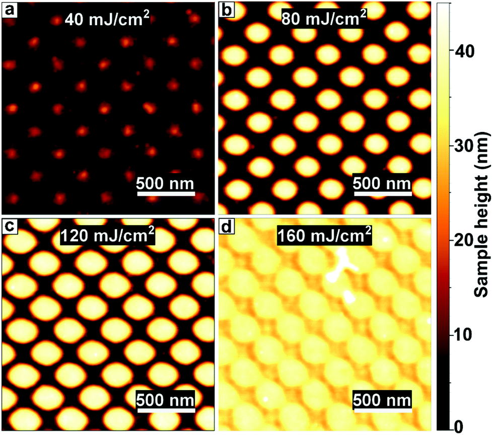 | ||
| Fig. 3 AFM image of PbS pillars exposed to different doses of EUV light. (a) Low doses lead to thin features remaining after development, (b and c) with good feature size and contrast between 80–120 ± 15 mJ cm−2. (d) At very high doses the feature dimension increases due to overexposure. | ||
Since the onset of cross-linking was hard to define by AFM because of the absence of a sharp edge, photoluminescence (PL) measurements were performed on EUV-exposed CdSe films as an accurate probe suitable for very thin films (Fig. 4a and b). An appreciable PL is detected for doses as low as 19.7 mJ cm−2, consistent with the optical microscopy images (Fig. S5†). The PL intensity increases with increasing dose, as a thicker film of QDs remains on the substrate. This increase in PL plateaus at doses over 280 mJ cm−2 (Fig. 4b and Fig. S5†). EUV doses higher than 280 mJ cm−2 do not lead to significant changes in PL intensity.
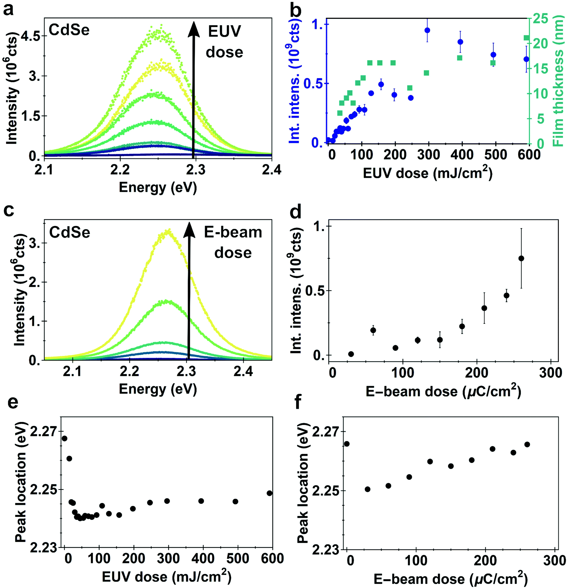 | ||
| Fig. 4 Photoluminescence spectra of CdSe films after exposure with EUV (a) or e-beam (c) and development. The integrated PL intensity as function of EUV (b) or e-beam (d) shows an increase in PL intensity as function of the exposure dose, which is related to the increased thickness of the remaining quantum dot film. Error bars indicate spread between multiple measurements on the same sample. (e) Position of peak fluorescence of CdSe films after exposure to EUV and (f) e-beam and development. Exposure leads to an initial red-shift, followed by a small blue-shift. | ||
The PL of e-beam exposed CdSe films shows a similar behavior as the EUV exposed films (Fig. 4c and d). PL intensity is increasing with increasing dose, due to thicker QD films remaining. Doses as low as 20 μC cm−2 are already enough to cross-link a small amount of quantum dots and measure appreciable PL intensity. At high doses one might expect beam damage affecting the emission intensity, for instance due to removal of ligands which would reduce surface passivation, but for the dose range tested we do not observe a decrease in intensity. As the film thickness continues to increase, the PL intensity also increases, even at doses >200 μC cm−2 which is on the high end of the exposure doses.
We fit the PL curves with a Gaussian profile to extract both the peak location (Fig. 4e and f) and full width at half maximum (FWHM) as a function of the dose (shown in ESI, Fig. S5†). For both EUV and e-beam exposed samples we observe an initial red-shift, followed by a small blue-shift in the emission energy as dose increases. The initial red-shift occurs in the dose range where cross-linking starts. Cross-linking of the QD ligands may reduce the interparticle spacing. This reduction enhances the energy transfer between the nanocrystals via the Förster Resonance Energy Transfer (FRET) that favors emission from lower-bandgap quantum dots.37–40 As the efficiency of energy transfer is strongly dependent of the distance between the two dipoles, small differences in interparticle distance in the order of several Å can already lead to such small red-shifts in the spectrum of photoluminescence.41 The reduction in interparticle spacing also increases the electronic coupling between dots, reducing the quantum confinement.37–40,42,43 We attribute the blue-shift at higher doses to a slight etching of the quantum dot surface by the high dose of highly energetic electrons. This removal of only a few surface atoms reduces the size of the QD core, leading to an effectively smaller crystal with more confinement, while not necessarily changing the radiative lifetimes.44 The blue-shift we observe (10–20 meV) corresponds to less than 0.1 nm reduction in QD radius.45 Another explanation for the blue-shift could be related to a change in the electronic environment, which is mainly a function of the ligands. A change in the electronic environment would require either (i) ligand removal, (ii) a change in the binding of the ligands to the surface or (iii) a change in their chemistry. FTIR indicates that the intensity of CH2/CH3 as well as the binding group remain unaffected, excluding (i) and (ii). Cross-linking could indeed form a larger barrier for the electronic wavefunction, and hence leading to a blue-shift. However, this change would be counter intuitive as cross-linking should reduce the (average) chain length leading to a red-shift instead.
The PL intensity scales with the film thickness (Fig. S6†), which is an indication that the photoluminescence quantum yield (PLQY) is relatively independent of dose. The PLQY is the ratio of radiative decay rate to the total decay rate (radiative + non-radiative decay). The non-radiative decay is mainly mediated by trap states due to imperfect surface passivation or changes in the electronic environment of the surface.46,47 This surface passivation arises from ligands binding to the surface. One would thus assume that a change to the ligand shell may affect the PLQY. Even a small fraction of ligand release would induce a large density of traps. Milder changes such as cross-linking may also change the PLQY, for instance because the refractive index of the ligands will change slightly. Also, cross-linking by aggregation of nanocrystal cores should red-shift the emission strongly due to an effective growth of the crystal and reduction of the confinement.48 The stability of the signal from the binding group we found earlier in FTIR is consistent with minimal changes to the ligand anchoring on the quantum dot surface.
Photoluminescence lifetime measurements are an accurate way of quantifying changes in non-radiative recombination.49 We recorded lifetime traces of CdSe QD films exposed to different doses of EUV light and e-beam irradiation after development using a Time Correlated Single Photon Counting (TCSPC) setup. Lifetime traces for EUV and e-beam exposed samples are shown in Fig. 5a and b respectively. Although decay traces of quantum dots in solution or single quantum dots commonly exhibit a single exponential decay, multi-exponential decay behavior is often found in solid-state ensembles of quantum dots.50–52 Similar to previous work we observe a bi-exponential decay consisting of one stretched exponential term:  .53Fig. 5c shows the different lifetime components for EUV exposure as function of the exposure dose. We can observe a small initial decrease in lifetime for both τ1 and τ2, which is consistent with the enhanced interparticle energy transfer described above. Above 200 mJ cm−2 we observe a slow increase in τ1 with increasing dose. For e-beam exposed samples of a different batch of QDs we also find that lifetimes are relatively stable upon exposure (lifetimes τ1 = 2.5 ± 0.25 ns, τ2 = 1.7 ± 0.5 ns, Fig. 5d). The stretched exponential exponent β, shown in ESI Fig. S10,† as function of dose, also appears to be stable at β = 0.29 ± 0.01 for EUV exposure and β = 0.36 ± 0.018 for e-beam exposure. We use these lifetime components to estimate a relative change in internal PLQY (see ESI, section S8†), and find that upon EUV exposure PLQYint drops by 20–50%, while e-beam exposure yields a relative increase in PLQYint. It should be noted however, that this analysis assumes no changes in outcoupling, which could affect the results. Although a small decrease in PLQY is observed, we would argue that the exposure is relatively mild to the CQD cores and these issues are likely mitigated by growing shells or using a repassivation step.
 | ||
| Fig. 5 PL lifetime traces of (a) EUV and (b) e-beam exposed CdSe films after development. Fitted lifetime components of the (c) EUV and (d) e-beam exposed films as function of dose. Radiative lifetimes become shorter after exposure, but are remarkably stable after the initial decrease. | ||
Both EUV photons and EBL electrons are very energetic in comparison to the visible spectrum. In order to investigate the minimum energy required to give rise to the chemical changes inducing a solubility switch, we exposed the quantum dot layers to less energetic radiation, in the form of Low Energy Electrons (LEE, 0–70 eV) and (deep-)UV ((D)UV) light (λ = 365 nm, 3.4 eV, and λ = 225 nm, 5.5 eV).
Fig. 6 shows the average height of a developed CdSe film as function of dose and electron energy, based on AFM measurements (Fig. S12†). We can already observe changes to the material at electron energies of 3 eV. Increasing the dose does not seem to have a significant influence on the changes in the material as these doses are high enough to insolubilize the whole film. At these low energies larger doses are necessary for cross-linking than in the case of 50 kV electrons, indicating that the cross-linking process may be less efficient at lower energies.
 | ||
| Fig. 6 Thickness of CdSe films after exposure to low-energy electrons and development. Depending on the dose, 3 eV electrons can already lead to a solubility switch of the QD film. | ||
Using lower-energy photons by DUV exposure is also possible. Previously Wang et al. already showed that (D)UV or blue light (λ = 254, 365, 405, 450 nm, 4.9, 3.4, 3.06, 2.75 eV) can be used for patterning QDs covered with photoactive ligands, as these molecules are unstable and degrade under exposure and their destruction leads to colloidal instability of the QDs.16,17 As the mechanism of the solubility switch is different in our case (cross-linking), it is not obvious whether DUV is energetic enough to induce this change. Exposure to 365 nm from a Suss MA6 mask aligner was unsuccessful. The intended pattern would not remain on the substrate, indicating that no chemical conversion was achieved. More energetic λ = 225 nm (5.5 eV) UV light from a Nd:YAG-laser (NT342B, Ekspla) did induce a solubility switch, however only at very high doses of 4000 mJ cm−2 (see ESI, Fig. S13†), which is two orders of magnitude higher than for EUV photons. This difference shows that the energy threshold for converting the material is different for photons and electrons, presumably because the way they induce chemical reactions is different. Photons with energies below the ionization energy promote only resonant electronic transitions. Therefore, if the relaxation process of these bound states does not lead to any bond cleavage, no chemical reaction can occur. Electrons on the other hand can also generate radicals which may allow chemical changes at lower energy. Despite this difference, the fact that both electrons and photons lead to chemical changes shows that our patterning mechanism is versatile and universal. As long as a minimum energy threshold is reached, 3 eV for electrons and 5.5 eV for photons, as-prepared quantum dots can be cross-linked to pattern them at micron- and nanoscale. We can see however, that the higher energy of the EUV photons allows for a more efficient crosslinking, possibly due to the fact that one absorbed EUV photon can create multiple reactive species that may crosslink more QDs simultaneously, requiring less photons for full conversion.
Finally, we demonstrate the versatility and the intricate patterns possible by directly patterning as- synthesized CdSe quantum dots into a miniature version of the painting “The Girl with the Pearl Earring” by Johannes Vermeer (Fig. 7a). This image was first pixelated, and the gray value was translated into the filling fraction of the individual pixel, which was then used for e-beam exposure. Fig. 7b shows that also this complex developed structure shows bright PL, demonstrating the feasibility of directly pattering active semiconductor quantum dots for complex optoelectronic devices. Next to this complexity, we believe it should be possible to pattern monolayers or double layers of CQDs, for instance by crosslinking the ligands to functionalizing molecules on the substrate. Here it will be key to make use of this functionalization to create selective adhesion of the CQDs to the substrate.
 | ||
| Fig. 7 (a) Optical microscope image of “The Girl With the Pearl Earring” (Johannes Vermeer, Mauritshuis Den Haag, NL) patterned in CdSe quantum dots with e-beam. (b) Fluorescence map of the remaining CdSe quantum dot film. (Excitation wavelength λ = 405 nm, detected emission λ = 545 nm.) Note that the color scale is reversed, as the luminescence of the QDs yields a negative image. | ||
Conclusions
We show a general one-step nanopatterning technique for as-synthesized PbS and CdSe quantum dots with several types of radiation. Both relatively low-energy photons (from 5.5 eV) as well as electrons (from 3 eV) can be used for patterning, as well as higher-energy EUV photons (91.9 eV) and highly energetic electrons (50 keV). Features can be as small as 60 nm which roughly corresponds to about 10 QDs in diameter. We find that the solubility change is achieved by cross-linking the organic ligands, to create a cohesive quantum dot film. Required doses are relatively low and in the same range as commercial state-of-the-art patterning materials (∼120 mJ cm−2 for EUV, ∼100 μC cm−2 for e-beam) and optimizing ligand chemistry might improve the sensitivity even further. The exposure to energetic electrons and extreme-UV photons, even to relatively high doses, does not significantly affect the luminescent properties. The versatility and simplicity of the technique allows for intricate designs at both nano- and micron scale. This simple, universal patterning technique can open a route to numerous applications with active semiconductors patterned on the nanoscale.Experimental methods
Chemicals
Lead oxide (PbO, 99.995%), selenium (Se, 99.999% pure), n-octane (>98%) were purchased from Alfa Aesar. Hexane (anhydrous) and toluene (anhydrous) were purchased from VWR. Bis(trimethylsilyl)sulphide (TMS, >98%), cadmium oxide (CdO, 99.99%), 1-octadecene (ODE, technical grade 90%), oleic acid (OA, technical grade 90%), acetone (ACE, analytical grade), isopropanol (IPA, analytical grade), methanol (analytical grade), sulfuric acid (H2SO4, 97.5%) and hydrogen peroxide (H2O2, 30%) were purchased from Sigma Aldrich. Double-side polished silicon wafers were purchased from Siegert Wafer.Nanocrystal synthesis
PbS nanocrystals were synthesized following Barkhouse et al.54 In a typical synthesis of PbS quantum dots, 0.45 g of PbO was added to 1.51 mL of OA to 18 mL of ODE into a three-neck flask. The solution was degassed at 100 °C for 3 hours under vacuum. All the powder dissolves, resulting in a clear solution. A second precursor was prepared by adding 0.213 mL of TMS to 10 mL of ODE. The lead precursor was heated to 120 °C. When the temperature was stable, the sulphur precursor was injected quickly and PbS quantum dots nucleate, resulting in a black solution. The reaction was quenched after about 30 seconds by injecting 20 mL of cold hexane and removing the flask from the heat, resulting in crystals of about 2 nm in size. After cooling to room temperature, the nanocrystals were washed three times by precipitation in ACE (first wash) and IPA (second, third wash), followed by centrifugation, discarding of the supernatant and redispersion in toluene. Finally the quantum dots were stored in octane at the desired concentration.Synthesis of the CdSe quantum dots was done similar to Čapek et al.55 First a selenium precursor was prepared of 0.1 M elemental selenium in ODE inside a three-neck flask. In order to accelerate the dissolution, the solution was heated to 180 °C for 5 hours, yielding a clear, orange solution while hot and a clear, deep-golden colored solution upon cooling. A cadmium precursor was made by adding 0.0942 g CdO, 2.272 mL of OA and 24 mL of ODE in a three-neck flask. The solution was degassed for 1 hour at 100 °C under N2. The temperature was raised to 260 °C and the CdO fully dissolved to yield a clear, colorless solution. 7.2 mL of Se-ODE was injected into the solution, causing the temperature to drop to 230 °C. The reaction was left ongoing for 5 minutes at this temperature before quenching the reaction by placing the flask in ice water. In the initial washing step, a mixture of toluene, and a 1![[thin space (1/6-em)]](https://www.rsc.org/images/entities/char_2009.gif) :1 MeOH:IPA solvent mixture was used to precipitate the nanocrystals. Upon redispersion in toluene, MeOH:IPA solvent mixture was used two more times wash the solution. The final dispersion of the nanocrystals was in octane or toluene at the desired concentration.
:1 MeOH:IPA solvent mixture was used to precipitate the nanocrystals. Upon redispersion in toluene, MeOH:IPA solvent mixture was used two more times wash the solution. The final dispersion of the nanocrystals was in octane or toluene at the desired concentration.
Film preparation
Samples for EUV exposure were made by spin coating thin films of quantum dots onto clean silicon substrates. The substrates were cleaned by subsequent ultrasonic cleaning in soap water, DI water, ACE and IPA. After sonication the substrates were cleaned 30 min in acid piranha solution (7:3 vol H2SO4:H2O2) and finally 15 min ozone plasma. Quantum dot solutions with a concentration between 10 and 35 mg mL−1 were filtered (0.2 micron PTFE filter) and spin coated at 2500 rpm for 20 seconds, resulting in films with a thickness of around 20–100 nm.
EUV exposure and development
The films were exposed to 91.9 eV light from the Swiss Light Source synchrotron at the Paul Scherrer Institute. Transmissive diffractive gratings were used as masks to create interfering beams, leading to periodic patterns on the wafer-level, ranging from line patterns (M716 mask) and contact hole patterns (M73 mask) to open frame patterning large areas (0.5 × 0.5 mm2) through a pinhole. With the M73 mask the error on the tool factor is larger, resulting in an error in the reported doses of 10–15%.After exposure the samples were developed in toluene, hexane or octane for 10 seconds, followed by a dip in clean toluene and subsequently in IPA, before drying with N2. Open frame samples were subsequently characterized by AFM, FTIR, PL microscopy, and TCSPC. Patterned samples were analyzed by SEM and AFM.
High-energy e-beam exposure
E-beam exposure was done in a Raith Voyager commercial e-beam lithography system with a voltage of 50 kV, LC30 column mode with 0.135 nA beam current. Films were developed in toluene immediately after exposure.Low-energy electron exposure
Experiments on exposing the quantum dot samples to low-energy electrons were performed in Leiden University using the ESCHER LEEM experimental setup. The design of the setup is based on a commercial aberration-corrected LEEM SPECS P90 instrument. Exposure to electrons of well-controlled energy and dose was performed using a LEEM built-in beam blanking system. For each single exposure event the sample was exposed to electrons of known energy. The electron energy value was constant during each exposure event. After finishing the exposure the electron beam was blanked and the sample stage was moved to a new unexposed position. As the result a 2D array of exposed oval-shaped areas was created. Within the array the x-axis corresponds to a change of dose at constant electrons energy while the y-axis corresponds to changes of energy at constant dose. After the exposure, the sample was developed in toluene and resulting pattern was analyzed using AFM.(Deep) UV exposure
Two different sources of exposure were used for (Deep) UV exposure. Exposure at (365 nm, 3.4 eV) was performed on a Suss MA/BA6 mask aligner with a 1000 W Hg lamp as exposure source. Samples were exposed through a contact mask in hard contact mode at a 100 μm gap. Various exposures were made at 25 mW cm−2 for total doses up to 10000 mJ cm−2.
As second UV exposure source a deep UV laser was used, in the form of a tunable Ekspla NT342. A NL300 pump laser with Second and Third Harmonic Generators (SHG, THG) producing 355 nm light pumps a parametric oscillator with SHG to generate of 5 ns 225 nm (5.5 eV) light pulses at a repetition rate of 10 Hz. Laser power of 5.0 mW with a spot size radius of 2 mm was used. Samples were exposed directly to the laser spot, to obtain circular exposure spots with doses up to 4000 mJ cm−2.
Scanning electron microscope
Scanning Electron Microscope images were taken by a FEI Verios 460 at voltages between 5 and 10 kV at 100 pA.Atomic force microscopy
AFM images were taken on a Veeco Dimension 3100 (Bruker) in tapping mode at a frequency of 1 Hz and a Dimension Icon (Bruker) in tapping mode.Photoluminescence
Photoluminescence of samples was measured using a WITec alpha300 SR confocal microscope with 100× Zeiss objective (NA 0.9). A 405 nm Thorlabs S1FC405 fiber coupled laser diode was used as excitation source. A 405 nm notch filter was used to remove the laser light in the detection path which was coupled to the detector. Light is collected in reflection on a UHTC 300 VIS WITec spectrometer. The PL spectra were converted to the energy scale using a Jacobian transformation.56 The setup can be used to record single spectra as well as perform spatial PL mapping.Photoluminescence lifetime measurements
Fluorescence lifetimes were recorded with a home-built Time Correlated Single Photon Counting setup (PicoQuant PDL 828 “Sepia II” and a PicoQuant HydraHarp 400 multichannel) in an inverted microscope with an Olympus 60× Plan Apochromat water immersion objective. The samples were excited by a 485 nm laser (PicoQuant LDH-D-C-485), which was pulsed at a repetition rate of 0.5 MHz. The excitation laser signal was blocked in the detection path by a Thorlabs FEL-500 long-pass filter in combination with a 488-NF notch filter.Fourier transform infrared spectroscopy
FTIR samples were spin coated on double side polished silicon substrates with a thickness of 500 μm. Spectra were recorded in transmission with a Bruker Vertex 80v under vacuum conditions. Each spectrum is an average of 20 spectra with a resolution of 4 cm−1.Optical microscope
Optical microscope images were recorded with a Zeiss, AxioCam ICc 5 equipped with a 20×/0.2 objective.Abbreviations
| AFM | Atomic force microscopy |
| CQD | Colloidal quantum dot |
| DUVL | Deep ultraviolet lithography |
| EBL | Electron beam lithography |
| EUVL | Extreme ultraviolet lithography |
| FRET | Förster resonant energy transfer |
| FTIR | Fourier transform infrared spectroscopy |
| LEE | Low energy electrons |
| LEEM | Low energy electron microscopy |
| PL | Photoluminescence |
| PLQY | Photoluminescence quantum yield |
| SEM | Scanning electron microscopy |
| TCSPC | Time correlated single photon counting |
| XPS | X-ray photoelectron spectroscopy |
| YAG | Yttrium aluminium garnet |
Author contributions
All authors have given approval to the final version of the manuscript.Funding sources
The research leading to these results has received funding from the European Community's Seventh Framework Programme (FP7/2007–2013) under grant agreement no. 312284 (CALIPSO). This work has been carried out at AMOLF and ARCNL. ARCNL is public-private partnership of UvA, VU, NWO and ASML. This work is part of the research program of the Netherlands Organization for Scientific Research (NWO)Conflicts of interest
There are no conflicts to declare.Acknowledgements
The authors thank Sven Askes and Sander Wuister for providing feedback on the paper, Michaela Vockenhuber for technical support with EUV exposure, Fred Brouwer and Michiel Hilbers for the technical support with DUV exposure and Bob Drent for technical support during e-beam exposures, as well as Andrea Cordaro for designing the e-beam pattern of “The Girl With the Pearl Earring”. We acknowledge the Paul Scherrer Institut, Villigen, Switzerland for provision of synchrotron radiation beamtime at beamline XIL-II of the SLS (proposals 20182111 and 20190811).References
- X. Lan, O. Voznyy, F. P. García de Arquer, M. Liu, J. Xu, A. H. Proppe, G. Walters, F. Fan, H. Tan, M. Liu, Z. Yang, S. Hoogland and E. H. Sargent, Nano Lett., 2016, 16, 4630–4634 CrossRef CAS PubMed.
- R. Wang, X. Wu, K. Xu, W. Zhou, Y. Shang, H. Tang, H. Chen and Z. Ning, Adv. Mater., 2018, 30, 1704882 CrossRef PubMed.
- N. Kirkwood, B. Singh and P. Mulvaney, Adv. Mater. Interfaces, 2016, 3, 1600868 CrossRef.
- G. Azzellino, F. S. Freyria, M. Nasilowski, M. G. Bawendi and V. Bulović, Adv. Mater. Technol., 2019, 4, 1800727 CrossRef CAS.
- T. B. Hoang, G. M. Akselrod and M. H. Mikkelsen, Nano Lett., 2016, 16, 270–275 CrossRef CAS PubMed.
- X. Lin, X. Dai, C. Pu, Y. Deng, Y. Niu, L. Tong, W. Fang, Y. Jin and X. Peng, Nat. Commun., 2017, 8, 1132 CrossRef PubMed.
- V. Adinolfi, I. J. Kramer, A. J. Labelle, B. R. Sutherland, S. Hoogland and E. H. Sargent, ACS Nano, 2015, 9, 356–362 CrossRef CAS PubMed.
- D. M. Balazs, N. Rizkia, H.-H. Fang, D. N. Dirin, J. Momand, B. J. Kooi, M. V. Kovalenko and M. A. Loi, ACS Appl. Mater. Interfaces, 2018, 10, 5626–5632 CrossRef CAS PubMed.
- D. J. Norris, Nat. Photonics, 2019, 13, 230–232 CrossRef CAS.
- C. Huang, X.-B. Li, C.-H. Tung and L.-Z. Wu, Chem. – Eur. J., 2018, 24, 11530–11534 CrossRef CAS PubMed.
- C. R. Kagan, E. Lifshitz, E. H. Sargent and D. V. Talapin, Science, 2016, 353, 885 CrossRef CAS PubMed.
- H. Keum, Y. Jiang, J. K. Park, J. C. Flanagan, M. Shim and S. Kim, ACS Nano, 2018, 12, 10024–10031 CrossRef CAS PubMed.
- F. Prins, D. K. Kim, J. Cui, E. De Leo, L. L. Spiegel, K. M. McPeak and D. J. Norris, Nano Lett., 2017, 17, 1319–1325 CrossRef CAS PubMed.
- A. Capretti, A. Lesage and T. Gregorkiewicz, ACS Photonics, 2017, 4, 2187–2196 CrossRef CAS PubMed.
- T. S. Mentzel, D. D. Wanger, N. Ray, B. J. Walker, D. Strasfeld, M. G. Bawendi and M. A. Kastner, Nano Lett., 2012, 12, 4404–4408 CrossRef CAS PubMed.
- Y. Wang, I. Fedin, H. Zhang and D. V. Talapin, Science, 2017, 357, 385–388 CrossRef CAS PubMed.
- Y. Wang, J. A. Pan, H. Wu and D. V. Talapin, ACS Nano, 2019, 13, 13917–13931 CrossRef CAS PubMed.
- F. Palazon, Q. A. Akkerman, M. Prato and L. Manna, ACS Nano, 2016, 10, 1224–1230 CrossRef CAS PubMed.
- M. T. Reetz, M. Winter, G. Dumpich, J. Lohau and S. Friedrichowski, J. Am. Chem. Soc., 1997, 119, 4539–4540 CrossRef CAS.
- T. R. Bedson, R. E. Palmer, T. E. Jenkins, D. J. Hayton and J. P. Wilcoxon, Appl. Phys. Lett., 2001, 78, 1921–1923 CrossRef CAS.
- V. Nandwana, C. Subramani, Y.-C. Yeh, B. Yang, S. Dickert, M. D. Barnes, M. T. Tuominen and V. M. Rotello, J. Mater. Chem., 2011, 21, 16859 RSC.
- D. B. Dement, M. K. Quan and V. E. Ferry, ACS Appl. Mater. Interfaces, 2019, 11, 14970–14979 CrossRef CAS PubMed.
- F. Palazon, M. Prato and L. Manna, J. Am. Chem. Soc., 2017, 139, 13250–13259 CrossRef CAS PubMed.
- T. Kozawa and S. Tagawa, Jpn. J. Appl. Phys., 2010, 49, 30001 CrossRef.
- J. Torok, R. Del Re, H. Herbol, S. Das, I. Bocharova, A. Paolucci, L. E. Ocola, C. Ventrice Jr., E. Lifshin, G. Denbeaux and R. L. Brainard, J. Photopolym. Sci. Technol., 2013, 26, 625–634 CrossRef CAS.
- W. M. Haynes, D. R. Lide and T. J. Bruno, CRC Handbook of Chemistry and Physics - Reference Book of Chemical and Physical Data, CRC Press, Boca Raton, 97th edn, 2017 Search PubMed.
- A. Narasimhan, L. Wisehart, S. Grzeskowiak, L. E. Ocola, G. Denbeaux and R. L. Brainard, J. Photopolym. Sci. Technol., 2017, 30, 113–120 CrossRef CAS.
- E. C. Mattson, Y. Cabrera, S. M. Rupich, Y. Wang, K. A. Oyekan, T. J. Mustard, M. D. Halls, H. A. Bechtel, M. C. Martin and Y. J. Chabal, Chem. Mater., 2018, 30, 6192–6206 CrossRef CAS.
- L. Wu, M. Baljozovic, G. Portale, D. Kazazis, M. Vockenhuber, T. Jung, Y. Ekinci and S. Castellanos Ortega, J. Micro/Nanolithogr., MEMS, MOEMS, 2019, 18, 013504 CAS.
- L. Zhang, R. He and H. C. Gu, Appl. Surf. Sci., 2006, 253, 2611–2617 CrossRef CAS.
- A. R. Smith, W. Yoon, W. B. Heuer, S. I. M. Baril, J. E. Boercker, J. G. Tischler and E. E. Foos, J. Phys. Chem. C, 2012, 116, 6031–6037 CrossRef CAS.
- M. H. Zarghami, Y. Liu, M. Gibbs, E. Gebremichael, C. Webster and M. Law, ACS Nano, 2010, 4, 2475–2485 CrossRef CAS PubMed.
- L. Robinet and M.-C. Corbeil, Stud. Conserv., 2003, 48, 23–40 CrossRef CAS.
- B. Smith, Infrared Spectral Interpretation - A Spectral Approach, CRC Press, Boca Raton, 1999 Search PubMed.
- S. N. Maganov, V. Elings and M.-H. Whangbo, Surf. Sci., 1997, 375, L385–L391 CrossRef.
- C. A. Mack, J. Electrochem. Soc., 1987, 134, 148 CrossRef CAS.
- C. R. Kagan, C. B. Murray and M. G. Bawendi, Phys. Rev. B: Condens. Matter Mater. Phys., 1996, 54, 8633–8643 CrossRef CAS PubMed.
- C. R. Kagan, C. B. Murray, M. Nirmal and M. G. Bawendi, Phys. Rev. Lett., 1996, 76, 1517–1520 CrossRef CAS PubMed.
- S. A. Crooker, J. A. Hollingsworth, S. Tretiak and V. I. Klimov, Phys. Rev. Lett., 2002, 89, 18–21 CrossRef PubMed.
- K. Tai, W. Lü, I. Umezu and A. Sugimura, Appl. Phys. Express, 2010, 3, 035202 CrossRef.
- K. F. Chou and A. M. Dennis, Sensors, 2015, 15, 13288–13325 CrossRef PubMed.
- Y.-H. Kim, J.-S. Heo, T.-H. Kim, S. Park, M.-H. Yoon, J. Kim, M. S. Oh, G.-R. Yi, Y.-Y. Noh and S. K. Park, Nature, 2012, 489, 128–132 CrossRef CAS PubMed.
- K. J. Williams, W. A. Tisdale, K. S. Leschkies, G. Haugstad, D. J. Norris, E. S. Aydil and X.-Y. Zhu, ACS Nano, 2009, 3, 1532–1538 CrossRef CAS PubMed.
- A. Van Dijken, A. H. Janssen, M. H. P. Smitsmans, D. Vanmaekelbergh and A. Meijerink, Chem. Mater., 1998, 10, 3513–3522 CrossRef CAS.
- J. Jasieniak, L. Smith, J. van Embden, P. Mulvaney and M. Califano, J. Phys. Chem. C, 2009, 113, 19468–19474 CrossRef CAS.
- M. A. Boles, D. Ling, T. Hyeon and D. V. Talapin, Nat. Mater., 2016, 15, 141–153 CrossRef CAS PubMed.
- A. J. Houtepen, Z. Hens, J. S. Owen and I. Infante, Chem. Mater., 2017, 29, 752–761 CrossRef CAS.
- R. Ihly, J. Tolentino, Y. Liu, M. Gibbs and M. Law, ACS Nano, 2011, 5, 8175–8186 CrossRef CAS PubMed.
- I. S. Nikolaev, P. Lodahl, A. F. van Driel, A. F. Koenderink and W. L. Vos, Phys. Rev. B: Condens. Matter Mater. Phys., 2007, 75, 115302 CrossRef.
- G. Schlegel, J. Bohnenberger, I. Potapova and A. Mews, Phys. Rev. Lett., 2002, 88, 4 CrossRef PubMed.
- B. R. Fisher, H. J. Eisler, N. E. Stott and M. G. Bawendi, J. Phys. Chem. B, 2004, 108, 143–148 CrossRef CAS.
- B. C. Fitzmorris, J. K. Cooper, J. Edberg, S. Gul, J. Guo and J. Z. Zhang, J. Phys. Chem. C, 2012, 116, 25065–25073 CrossRef CAS.
- O. Schöps, N. Le Thomas, U. Woggon and M. V. Artemyev, J. Phys. Chem. B, 2006, 110, 2074–2079 CrossRef PubMed.
- D. A. R. Barkhouse, R. Debnath, I. J. Kramer, D. Zhitomirsky, A. G. Pattantyus-Abraham, L. Levina, L. Etgar, M. Grätzel and E. H. Sargent, Adv. Mater., 2011, 23, 3134–3138 CrossRef CAS PubMed.
- R. K. Čapek, I. Moreels, K. Lambert, D. De Muynck, Q. Zhao, A. Van Tomme, F. Vanhaecke and Z. Hens, J. Phys. Chem. C, 2010, 114, 6371–6376 CrossRef.
- J. Mooney and P. Kambhampati, J. Phys. Chem. Lett., 2013, 4, 3316–3318 CrossRef CAS.
Footnote |
| † Electronic supplementary information (ESI) available. See DOI: 10.1039/d0nr01077d |
| This journal is © The Royal Society of Chemistry 2020 |