
 Open Access Article
 This Open Access Article is licensed under a Creative Commons Attribution-Non Commercial 3.0 Unported Licence
Quantitative measurement of charge accumulation along a quasi-one-dimensional W5O14 nanowire during electron field emission†
Fengshan
Zheng
 *a,
Giulio
Pozzi
ab,
Vadim
Migunov
c,
Luka
Pirker
d,
Maja
Remškar
d,
Marco
Beleggia
e and
Rafal E.
Dunin-Borkowski
a
*a,
Giulio
Pozzi
ab,
Vadim
Migunov
c,
Luka
Pirker
d,
Maja
Remškar
d,
Marco
Beleggia
e and
Rafal E.
Dunin-Borkowski
a
aErnst Ruska-Centre for Microscopy and Spectroscopy with Electrons and Peter Grünberg Institute, Forschungszentrum Jülich, 52425 Jülich, Germany. E-mail: f.zheng@fz-juelich.de
bDepartment of Physics and Astronomy, University of Bologna, Viale Berti Pichat 6/2, 40127 Bologna, Italy
cCentral Facility for Electron Microscopy (GFE), RWTH Aachen University, Ahornstrasse 55, 52074 Aachen, Germany
dJozef Stefan Institute, Solid-State Physics Department, Jamova 39, SLO-1000 Ljubljana, Slovenia
eDTU Nanolab, Technical University of Denmark, 2800 Kgs. Lyngby, Denmark
First published on 6th March 2020
Abstract
We use an electron holographic method to determine the charge distribution along a quasi-one-dimensional W5O14 nanowire during in situ field emission in a transmission electron microscope. The results show that the continuous charge distribution along the nanowire is not linear, but that there is an additional accumulation of charge at its apex. An analytical expression for this additional contribution to the charge distribution is proposed and its effect on the field enhancement factor and emission current is discussed.
1 Introduction
Field emission is important for many applications, including the development of coherent electron sources for electron microscopy.1,2 There has been interest in using nanotubes, nanocones and nanowires as field emitters, as a result of the enhanced field strength at their high aspect ratio tips.3–6 The field enhancement factor, which provides a measure of how much stronger the electric field is at the apex of an emitter than the applied field, is a crucial parameter that describes field emission characteristics.7 A quantitative understanding of the factors that determine the enhancement factor of a field emitter is essential for providing deeper insights into the field emission process. Several analytical approaches8–10 have been proposed to predict field enhancement factors. However, they typically require assumptions about the shape of the emitter, as well as a knowledge of the distance between its apex and the counter-electrode. The charge distribution along a field emitter is often assumed to follow a line charge model (LCM),9,11–13 in which the line charge density is constant, linear or nonlinear,10 depending on the shape of the equipotential surface around the emitter, i.e., on its geometrical shape. However, the validity of such assumptions is rarely based on direct experimental evidence. The spatially-resolved measurement of charge distributions along such nanostructures is therefore essential in order to validate the LCM, measure the enhancement factors of field emitters that have realistic shapes and provide guidelines for the synthesis, development and optimisation of novel field emitters.Here, we use off-axis electron holography to measure the charge distribution along a one-dimensional W5O14 nanowire that is subjected to an external electrical bias in situ in a transmission electron microscope (TEM). We find that, as a result of the nearly cylindrical shape with a large aspect ratio of the nanowire, additional charges accumulate at its apex, with the charge distribution varying nonlinearly with distance. A linear charge density model is therefore inadequate to describe the charge distribution along the length of such a nanowire, in particular close to its apex.
In order to model the charge distribution and accurately fit the experimental data, we propose an empirical expression for a nonlinear correction to the charge density, which has been inspired by the use of discrete charges to approximate the continuous charge density along a cylindrical needle.14 The influence of this nonlinear term on the field enhancement factor and emission properties of the nanowire is considered by assuming the standard geometry10 of a smooth axially-symmetric emitter mounted perpendicularly on a conducting plane in the presence of an electric field that is asymptotically uniform and parallel to the emitter axis. We discuss the dependence of the field enhancement factor and emission current on the shape of the wire, which is determined by the ratio between the linear and additional contributions to the charge distribution. We compare these predictions with our measurements of field emission performed in situ in the TEM.
2 Experimental methods
Off-axis electron holography15,16 is an interferometric technique, which is based on the superposition of an object wave that travels through a region of interest in the TEM with a reference wave that travels through a nearby region of vacuum, in order to form an interference pattern in the image plane, from which the phase and amplitude of the object electron wavefunction can be retrieved. The technique has been used to map long-range electric and magnetic fields.17 However, care is required in such experiments if the reference wave is perturbed by fringing fields that originate from the sample itself.18In the absence of magnetic fields and assuming that dynamical diffraction in the specimen can be neglected, the phase of the object wave can be written in the form:
 | (1) |
 | (2) |
3 Results
W5O14 nanowires, which are promising field emitters,25–27 were synthesised to have lengths of several tens of μm, widths of ∼60–100 nm, quasi-rectangular cross-sections and sharp ends, as shown in the form of a low-magnification scanning electron microscopy (SEM) image in Fig. 1a. We measured the charge distribution along an individual electrically-biased W5O14 nanowire with a length of 10 μm and a width of 80 nm, which was mounted in a scanning tunnelling microscopy (STM)-TEM holder from Nanofactory Instruments28 and examined in an FEI Titan 60–300 TEM operated at 300 kV. The nanowire was mounted on the fixed side of the holder, while an electrochemically-sharpened W wire was used as the counter-electrode on the movable side. The separation between the apex of the nanowire and the counter-electrode was set to be approximately 1.5 μm, as shown in Fig. 1b. The nanowire was found to be contaminated slightly by an approximately 10 nm-thick amorphous layer (see Fig. S1 in the ESI†). Fig. 1c and d show a representative phase image and a corresponding phase contour map recorded with the nanowire electrically biased at 150 V. The phase contours in Fig. 1d are asymmetrical with respect to the nanowire axis, primarily due to the influence of the perturbed reference wave,29 as the strong electric field of the nanowire penetrates into vacuum and affects the vacuum reference wave.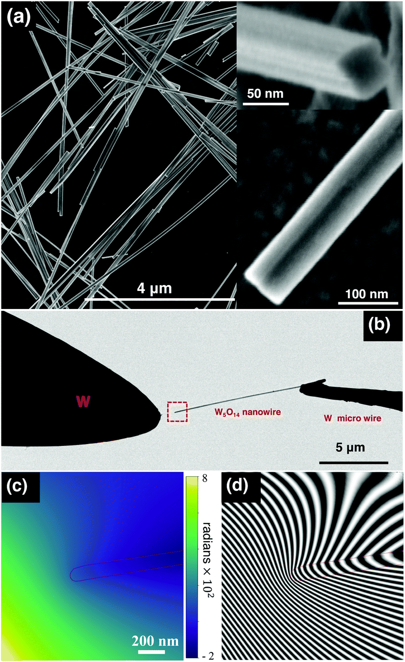 | ||
| Fig. 1 Experimental electrical biasing setup: (a) Low magnification SEM image of W5O14 nanowires and two higher magnification images of individual nanowires in longitudinal and cross-sectional viewing directions; (b) bright-field TEM image showing the geometry of the setup for characterising an electrically-biased W5O14 nanowire, with a red rectangle showing the region studied using off-axis electron holography; (c and d) representative electron optical phase image and corresponding phase contour map of the W5O14 nanowire shown in (b) examined under an applied electrical bias of 150 V. The outline of the nanowire is marked by a red line in (c) and (d). The phase contour spacing in (d) is 8π radians. The mean inner potential contribution to the phase was not removed in (c) and (d). | ||
3.1 Field emission current
In order to study electron field emission from the nanowire in situ in the TEM, the current was monitored as a function of applied voltage. The measured current–voltage dependence (I–V curve) is plotted in Fig. 2. The emission current was observed to fluctuate after the onset of field emission at approximately 148 V. The magnitudes of these fluctuations are shown in the form of error bars in Fig. 2. At each voltage, the emission current was measured for up to 1 s collecting at every 0.05 s (i.e., 20 data points in total). The fluctuations in measured current were not observed to be associated with corresponding fluctuations in electrostatic potential or electric field. Indeed, no double exposure (i.e., Moiré) effects30,31 were observed in electron holograms recorded using 6 s exposure times, whether or not the nanowire was field emitting. In addition to the instabilities, the emission current started to drop at an applied bias of 180 V and stopped completely at 188 V (see the ESI† for further details). The inset to Fig. 2 shows a so-called Fowler–Nordheim (F–N) plot. Between 148 and 180 V, there is an approximately linear relationship between and
and  , in agreement with the Fowler–Nordheim theory of electron field emission.7 The field enhancement factor can be estimated from the F–N plot to be approximately 350. If the onset voltage for field emission is assumed to be 148 V, then the local electric field can be inferred to be 4.90 V nm−1 (see the ESI† for further details).
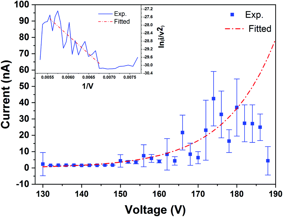 | ||
Fig. 2 Field emission current I measured in situ in the TEM as a function of applied bias voltage V for the W5O14 nanowire (blue). The red dot-dashed line shows an exponential profile fitted to the data between 130 and 180 V. The inset shows a corresponding F–N plot (blue), with  plotted as a function of plotted as a function of  determined from the measured I–V data. The red dot-dashed line in the inset shows a linear fit to values between 148 and 180 V. determined from the measured I–V data. The red dot-dashed line in the inset shows a linear fit to values between 148 and 180 V. | ||
3.2 Cumulative charge profiles
Applied-bias-dependent cumulative charge profiles along the nanowire were evaluated from the total electron phase shift measured at each applied bias voltage by using eqn (2) (see the ESI† for a discussion of the influence of the MIP contribution to the phase on the evaluation of the cumulative charge). The integration region around the nanowire, which is marked by a red rectangle in the top panel of Fig. 3, was allowed to shrink in the direction indicated by the red arrow to determine the cumulative charge along the nanowire. The cumulative charge profiles along the nanowire for different applied bias voltages from its apex are shown in the main panel of Fig. 3. | ||
| Fig. 3 Cumulative charge profiles along the W5O14 nanowire measured from electron optical phase images for applied bias voltages of 130 to 186 V. The top panel shows the MIP contribution to the phase (recorded in the absence of an applied electrical bias), with the integration region marked. The y-axis points to the right. The origin is chosen to be at the left edge of the image. The inset shows the total charge in the chosen region of the nanowire plotted as a function of applied bias voltage (red squares) and a linear fit to these values (blue line). | ||
The total charge in the selected region (the red rectangle marked in Fig. 3), i.e., the value at y = 0 nm in the chosen reference system, increases linearly with applied bias voltage, as shown in the inset to Fig. 3. This measurement allows the capacitance of this part of the nanowire to be determined to be 8.78 ± 0.04 aF. The fact that the cumulative charge changes in a quasi-parabolic manner as the width of the integration region is decreased suggests that the charge density along the nanowire is approximately linear. However, Fig. 4a shows that the experimental cumulative charge profile (red) deviates significantly from the parabolic trend (blue) approximately 300 nm from the apex of the nanowire. In Fig. 4a, a best quadratic fit to the cumulative charge profile for an applied electrical bias voltage of 150 V was determined from values measured more than 300 nm from the apex of the nanowire. This result shows directly that there is an accumulation of charge at the apex of the nanowire in the presence of an applied electrical bias. Note that the presence of crystallographic facets or edges is expected to have an influence on the charge distribution at the edges of the nanowire. However, it is not straightforward to identify their contributions in the present study, both because of the limited spatial resolution of approximately 5 nm and because of the mean inner potential contribution to the recorded phase images (see the ESI† for details).
 | ||
| Fig. 4 Fitting of cumulative charge profile based on a nonlinear line charge model: (a) Comparison between experimentally measured cumulative charge profile (black) and best fits based on a nonlinear line charge model described by eqn (3) (red) and a 2nd order polynomial fit (blue); (b) line charge density along the nanowire obtained from the best-fitting parameters based on eqn (3). The nanowire was electrically biased at 150 V. | ||
4 Theoretical analysis
In previous experimental studies of biased carbon nanotubes20 and sharp metallic needles,32,33 it was shown that a linear or constant charge density distribution is associated with a tip shape, whose equipotential surface is similar to that of a paraboloid or ellipsoid of rotation. Such shapes are markedly different from that of the present nanowire, which has a larger aspect ratio and can be described more closely as a cylinder on the assumption of rotational symmetry.A similar accumulation of charge to that observed here has been thoroughly discussed in a series of didactic papers about the equilibrium charge distribution along a conducting needle.14,34,35 These works have highlighted the influence of the detailed shape of the needle on the charge distribution along it.
In particular, Griffiths and Li,14 inspired by the treatment of a finite cylinder by Smythe,36 proposed an empirical analytical expression for the charge density in a needle. Based on their work and by limiting our considerations to the tip of the nanowire, we propose that the line charge density λ in our nanowire takes approximately the following form, which comprises a constant term C, a linear term Dy and a divergent term  that corresponds to the “fundamental term” in Smythe's expansion:36
 | (3) |
 | (4) |
Eqn (4) fits our experimental measurements very well, as shown in Fig. 4a for an applied bias voltage of 150 V (see Fig. S3 and Table S1 in the ESI† for details of the fits to all the experimental measurements). The corresponding line charge density along the nanowire, which can be plotted by using the best-fitting parameters as shown in Fig. 4b, reveals the divergence of charge density at its apex.
Although the close fit provides strong evidence for the validity of eqn (4), we are not able to provide values of the fitting parameters for the full length of the nanowire due to the limited field of view in the recorded holograms. In order to infer this information from the present measurements and to assess the relative weights of the linear and additional contributions to the field enhancement factor, we assume here the standard geometry of a line charge distribution that protrudes perpendicular to a conducting plane in the presence of an electric field that is asymptotically uniform and parallel to the direction of the line charge.9–11 For a linear charge distribution, the surface that corresponds to V = 0 has the shape of a hemi-ellipsoid and is suitable for representing the surface of a field emitter that has such a shape. We used a similar procedure here to assess the effect on the field enhancement factor of adding a nonlinear term (i.e., the divergent term in eqn (3)) to a linear charge distribution. Satisfyingly, the additional nonlinear term changes the shape of the equipotential surface from an elongated ellipsoid to a rounded cylinder (see the ESI† for further details).
4.1 Field enhancement factor and emission current
We now assume that the length of the line charge is equal to that of the nanowire (i.e., A = 9.4 μm) and that the charge density vanishes at the conducting plane (i.e., λ(0) = 0). We express the remaining parameters in terms of the total charge in the linear contribution, qlin, as well as the additional (i.e., nonlinear) term, qtip. The expression for the line charge density in eqn (3) becomes: | (5) |
The electrostatic potential and electric field can then be calculated based on image charge theory. Here, we fix the radius of the nanowire at its base (in this case, 40 nm). We are left with the ratio between the linear and nonlinear terms (taking qtip = 1) as a free parameter, which affects the overall shape of the nanowire. Once this is fixed, the knowledge of the electric field at any position on the surface of the nanowire allows us to calculate the field enhancement factor and, upon further integration, the emission current from the Fowler–Nordheim expression (see the ESI† for further details).
The results are shown in Fig. 5a–c, where attention is focused on the region around the tip where emission takes place, in the form of two-dimensional maps of the magnitude of the electric field for ratios between the linear and nonlinear terms of 4, 5 and 6, respectively. In each case, the black area represents the shape of the tip and the transition from a smoother to a sharper tip is evidenced by the radius at the basis. The maximum value at the apex gives the field enhancement factor, as shown in Fig. 5d–f, which illustrate more quantitatively the trend of the electric field along the axis from the apex. The field enhancement factor is approximately 340 when the ratio is 5, which is close to the experimental estimate of ∼350. Fig. 5g–i show the calculated emission current plotted as a function of the applied bias voltage for the above ratios (see the ESI† for details about the field emission calculations). Despite the use of several assumptions and the relative simplicity of the model, it is encouraging that the result for a ratio of 5 is in good agreement with our experimental measurements (Fig. 2).
 | ||
| Fig. 5 Simulations based on a nonlinear charge density model: (a)–(c) Electric field maps in the central slice. The black shadow marks the apex of the nanowire (the rest of the nanowire is not shown); (d)–(f) field enhancement factors along the axis of the nanowire (indicated by a red arrow in (a)); (g)–(i) field emission current for ratios between the linear and nonlinear contributions of 4, 5 and 6, respectively. A ratio of 5 delivers the most satisfying agreement with the experiments. | ||
5 Conclusions
In summary, off-axis electron holography has been used to determine the cumulative charge distribution along a W5O14 nanowire with 5 nm spatial resolution during in situ field emission carried out in the transmission electron microscope. Analysis of the data using analytical modelling reveals that a linear charge density model requires an additional nonlinear term to describe the accumulation of charge at the apex of the nanowire as a result of its elongated cylindrical shape. This additional nonlinear term can be described by an empirical expression, which corresponds to the “fundamental term” in an expansion by Smythe for the charge distribution in a cylinder.36 This analytical model provides good agreement with experimental values for the projected electrostatic potential and is used to calculate the field enhancement factor and emission current. The introduction of Smythe's term provides an extra degree of freedom which is able to improve, with respect to other analytical models, the correspondence between shape and emission properties of nanowires and could prove extremely valuable for the development of novel nanomaterial-based emitters for use as ultra-high brightness electron sources.6 Experimental details
6.1 Sample synthesis
Quasi-one-dimensional W5O14 nanowires were synthesised by the “iodine transport” method.25 The starting material consisted of 352.7 mg of WO3 powder (Sigma Aldrich, 99.99%), 37.5 mg of Ni (metal foil) and 567 mg of iodine (1–3 mm beads, Sigma Aldrich, 99.7%). WO3 was used as the source of tungsten and oxygen, while Ni was added as a growth promoter. Evacuated (4 × 10⁻⁶ mbar) and sealed quartz ampoules were inserted into a two-zone furnace for 500 hours. The material was transported from 860 °C to 736 °C. The morphologies of the nanowires were examined using scanning electron microscopy (SEM).6.2 Off-axis electron holography
Off-axis electron holograms were acquired with a direct electron detection Gatan K2-IS camera using an exposure time of 6 s. The interference fringe spacing was 2.4 nm (5.4 pixels), resulting in a spatial resolution of approximately 5 nm in reconstructed phase images. The width of the interference region was approximately 2 μm. Holograms were acquired from the apex of an individual nanowire for a range of applied bias voltages (between 0 and 188 V). Reference holograms were recorded from vacuum after shifting the specimen by at least 50 μm without applying a bias voltage. Reconstruction of holograms was performed using a standard Fourier-transform-based approach in Holoworks software (Holowerk LLC).Conflicts of interest
There are no conflicts to declare.Acknowledgements
The authors thank Prof. Michael Farle and AG Farle at the University of Duisburg-Essen for technical help, Maximilian Kruth for focused ion beam preparation of the specimen, Werner Pieper and Rolf Speen for technical assistance and Gatan, Inc. for cooperation within the framework of a scientific agreement. The authors acknowledge the European Union for funding through the Marie Curie Initial Training Network SIMDALEE2 (Marie Curie Initial Training Network (ITN) Grant No. 606988 under FP7-PEOPLE-2013-ITN) and through the Horizon 2020 Research and Innovation Programme under Grant agreement no. 823717-ESTEEM3. V. M. thanks the Deutsche Forschungsgemeinschaft for funding within the framework of the SFB 917 project Nanoswitches. R. E. D.-B. thanks the Deutsche Forschungsgemeinschaft for a Deutsch-Israelische Projektkooperation (DIP) Grant and the European Union's Horizon 2020 Research and Innovation Programme Q-SORT (Grant No. 766970 under H2020-FETOPEN-2016-2017).References
-
D. B. Williams and C. B. Carter, Transmission electron microscopy: A textbook for materials science, Springer, 1998 Search PubMed
.
-
L. Reimer, Scanning electron microscopy: Physics of image formation and microanalysis, Springer, 2013, vol. 45 Search PubMed
- W. A. de Heer, A. Châtelain and D. Ugarte, Science, 1995, 270, 1179–1180 CrossRef CAS
- N. de Jonge, Y. Lamy, K. Schoots and T. H. Oosterkamp, Nature, 2002, 420, 393 CrossRef CAS PubMed
- M. Žumer, V. Nemanič, B. Zajec, M. Wang, J. Wang, Y. Liu and L.-M. Peng, J. Phys. Chem. C, 2008, 112, 5250–5253 CrossRef
- F. Houdellier, A. Masseboeuf, M. Monthioux and M. J. Hÿtch, Carbon, 2012, 50, 2037–2044 CrossRef CAS
- R. H. Fowler and L. Nordheim, Proc. R. Soc. London, Ser. A, 1928, 119, 173–181 CAS
- R. G. Forbes, C. Edgcombe and U. Valdre, Ultramicroscopy, 2003, 95, 57–65 CrossRef CAS PubMed
- E. G. Pogorelov, A. I. Zhbanov and Y.-C. Chang, Ultramicroscopy, 2009, 109, 373–378 CrossRef CAS PubMed
- D. Biswas, Phys. Plasmas, 2018, 25, 043113 CrossRef
-
E. Durand, Électrostatique, Masson, Paris, 1964, vol. 2 Search PubMed
- J. Harris, K. Jensen, D. Shiffler and J. Petillo, Appl. Phys. Lett., 2015, 106, 201603 CrossRef
- J. Harris, K. Jensen and D. Shiffler, J. Phys. D: Appl. Phys., 2015, 48, 385203 CrossRef
- D. J. Griffiths and Y. Li, Am. J. Phys., 1996, 64, 706–714 CrossRef
-
A. Tonomura, Electron holography, Springer, 2nd edn, 1999 Search PubMed
- H. Lichte and M. Lehmann, Rep. Prog. Phys., 2007, 71, 016102 CrossRef
- G. Pozzi, M. Beleggia, T. Kasama and R. E. Dunin-Borkowski, C. R. Phys., 2014, 15, 126–139 CrossRef CAS
-
G. Matteucci, G. F. Missiroli and G. Pozzi, Advances in Imaging and Electron Physics, Elsevier, 2002, vol. 122, pp. 173–249 Search PubMed
- M. O'Keeffe and J. Spence, Acta Crystallogr., Sect. A: Found. Crystallogr., 1994, 50, 33–45 CrossRef
- M. Beleggia, T. Kasama, R. E. Dunin-Borkowski, S. Hofmann and G. Pozzi, Appl. Phys. Lett., 2011, 98, 243101 CrossRef
- C. Gatel, A. Lubk, G. Pozzi, E. Snoeck and M. J. Hÿtch, Phys. Rev. Lett., 2013, 111, 025501 CrossRef CAS PubMed
- M. Beleggia, L. Gontard and R. E. Dunin-Borkowski, J. Phys. D: Appl. Phys., 2016, 49, 294003 CrossRef
- V. Migunov, A. London, M. Farle and R. E. Dunin-Borkowski, J. Appl. Phys., 2015, 117, 134301 CrossRef
- F. Zheng, J. Caron, V. Migunov, M. Beleggia, G. Pozzi and R. E. Dunin-Borkowski, J. Electron Spectrosc. Relat. Phenom., 2020 DOI:10.1016/j.elspec.2019.07.002
- M. Remškar, J. Kovac, M. Viršek, M. Mrak, A. Jesih and A. Seabaugh, Adv. Funct. Mater., 2007, 17, 1974–1978 CrossRef
- G. Ulisse, C. Ciceroni, A. Carlo, F. Brunetti, J. Jelenc, M. Saqib, A. Varlec and M. Remskar, Microelectron. Eng., 2017, 170, 44–48 CrossRef CAS
- M. Saqib, J. Jelenc, L. Pirker, S. D. Škapin, L. De Pietro, U. Ramsperger, A. Knápek, I. Müllerová and M. Remškar, J. Electron Spectrosc. Relat. Phenom., 2020 DOI:10.1016/j.elspec.2019.03.005
- K. Svensson, Y. Jompol, H. Olin and E. Olsson, Rev. Sci. Instrum., 2003, 74, 4945–4947 CrossRef CAS
- G. Matteucci, G. Missiroli, M. Muccini and G. Pozzi, Ultramicroscopy, 1992, 45, 77–83 CrossRef
- V. Migunov, C. Dwyer, C. B. Boothroyd, G. Pozzi and R. E. Dunin-Borkowski, Ultramicroscopy, 2017, 178, 48–61 CrossRef CAS PubMed
- C. Gatel, F. Houdellier and E. Snoeck, J. Phys. D: Appl. Phys., 2016, 49, 324001 CrossRef
- M. Beleggia, T. Kasama, D. Larson, T. F. Kelly, R. E. Dunin-Borkowski and G. Pozzi, J. Appl. Phys., 2014, 116, 024305 CrossRef
- A. H. Tavabi, V. Migunov, C. Dwyer, R. E. Dunin-Borkowski and G. Pozzi, Ultramicroscopy, 2015, 157, 57–64 CrossRef CAS PubMed
- M. Andrews, Am. J. Phys., 1997, 65, 846–850 CrossRef
- J. D. Jackson, Am. J. Phys., 2000, 68, 789–799 CrossRef
- W. Smythe, J. Appl. Phys., 1956, 27, 917–920 CrossRef
Footnote |
| † Electronic supplementary information (ESI) available. See DOI: 10.1039/D0NR00739K |
| This journal is © The Royal Society of Chemistry 2020 |