
 Open Access Article
 This Open Access Article is licensed under a Creative Commons Attribution-Non Commercial 3.0 Unported Licence
Efficiency-enhanced and sidelobe-suppressed super-oscillatory lenses for sub-diffraction-limit fluorescence imaging with ultralong working distance†
Wenli
Li
abcd,
Pei
He
abcd,
Weizheng
Yuan
*abcd and
Yiting
Yu
 *abcd
*abcd
aResearch & Development Institute of Northwestern Polytechnical University in Shenzhen, Room 2501, No.45, Gaoxin South 9th Road, Nanshan District, Guangdong, Shenzhen 518057, China
bCollege of Mechanical Engineering, Northwestern Polytechnical University, Xi'an 710072, China
cKey Laboratory of Micro/Nano Systems for Aerospace (Ministry of Education), Northwestern Polytechnical University, Xi'an 710072, China
dShaanxi Province Key Laboratory of Micro and Nano Electro-Mechanical Systems, Northwestern Polytechnical University, Xi'an 710072, China. E-mail: yyt@nwpu.edu.cn; yuanwz@nwpu.edu.cn
First published on 6th March 2020
Abstract
Super-oscillatory lens (SOL) optical microscopy, behaving as a non-invasive and universal imaging technique, as well as being a simple post-processing procedure, may provide a potential application for sub-diffraction-limit fluorescence imaging. However, the low energy concentration, high-intensity sidelobes and micrometer-scale working distance of the reported planar SOLs impose unavoidable restrictions on the ground-state applications. Here, we demonstrate step-shaped SOLs based on the multiple-phase-modulated (MPM) method to improve the focusing efficiency. Two pivotal advantages are thus generated: (i) the fabrication complexity can be effectively reduced based on several conventional optical lithography steps; (ii) the focusing efficiency is much higher than that of the random MPM ones due to the efficient manipulation of the wavefronts, bringing about a stronger light concentration to the focal spot. Additionally, the ratio of the sidelobe intensity is flexibly tuned to meet the customized requirements, and a 2 mm-working-distance MPM SOL with the sidelobe intensity highly suppressed is finally exploited. For the first time, as far as we know, a SOL-based fluorescence microscopy without the pinhole filter to map the horizontal morphology of the dispersive fluorescent particles is established. Compared with the results achieved by the conventional wide-field microscopy, the sample details beating the diffraction limit can be reconstructed by simple imaging fusion. This research demonstrates the promising applications of SOLs for low-cost, simplified and highly customized sub-diffraction-limit fluorescence imaging systems free from photobleaching and an extremely short working distance.
Introduction
Super-resolution fluorescence microscopy is a powerful detection tool in the biotechnology and life science fields.1–4 Stimulated emission depletion microscopy (STED), structured illumination microscopy (SIM), photo-activated localization microscopy (PALM), and stochastic optical reconstruction microscopy (STORM) are able to provide resolution at tens of nanometers in far field through distinguishing the fluorophores.5–8 To selectively activate or deactivate fluorophores, high-energy laser, a mercury lamp and a xenon lamp are normally needed. Then, the fine physical details of the samples can be resolved by combining with a complicated high-resolution imaging post-processing algorithm. Notably, using a high-power laser to deplete the fluorophores in the ground state could induce strong photobleaching, and consequently damage the biological samples, restricting the in vivo applications.Recently, a non-invasive and universal imaging technique without complex mathematical post-processing, called super-oscillatory lens (SOL) optical microscopy, was proposed.9–15 The optical super-oscillation phenomenon is the delicate interference of far-field propagating waves carrying the fine physical details of objects, and it can be accurately engineered to achieve sub-diffraction-limit foci, even smaller than the size defined as the super-oscillatory criterion 0.38λ/NA (where NA is numerical aperture).16,17 However, the small super-oscillation hotspots are always accompanied by inevitably moderate sidelobes,18 bringing a certain inconvenience for practical applications, especially in fields that do not need too small a hotspot but a wide enough effective field of view for optical imaging. To achieve a reasonable balance among the lens size, subwavelength focal spot, extremely long working distance and relative weak sidelobes for practice, we confine the focal spot within the range between the super-oscillatory criterion and the Rayleigh criterion18,19 to customize the centimeter-scale planar super-resolution lens with a working distance of about 6 mm. The sub-diffraction-limit hotspots are achieved at a price of tremendous incident energy loss, but this exactly offers favorable conditions for usage in super-resolution fluorescence imaging without damaging the biological samples. Moreover, in the configuration of SOL fluorescence microscopy, only fluorophores within the sub-diffraction-limit excitation area can be stimulated implicitly, eliminating most out-of-focus fluorescence background signals and reducing the unwanted photobleaching.20,21 Additionally, the outstanding light-field customization capability of the SOLs endows many merits for far-field super-resolution imaging. One typical example is the flexible optimization method. We have established a universal optimization design model in our recent work to realize achromatic SOLs and achromatic-customized SOLs, which manifest satisfactory focusing patterns both experimentally and theoretically.22–25 Except for the characteristics that the light contours of the SOLs can be flexibly controlled, another unique advantage is that the ratio of focusing intensity can be customized as well. We have achieved the precise adjustment of the intensity ratio of multi-focal SOLs,23 which may offer potential possibility to customize the intensity ratio for different samples under specific requirements. Notably, parallel fabrication of optical elements is becoming the main trend instead of the complex and time-consuming processes such as electron beam lithography (EBL) and focused ion beam etching (FIB).15,26–29 Recently, direct laser writing (DLW) lithography was employed to fabricate a planar lens,30,31 but several square regions were joined together to acquire a hundreds of micrometers device and an apparent misalignment could be found. Through pushing the smallest line width of the planar SOLs up to tens of micrometers, we just realized centimeter-scale SOLs by employing the normal lithography process at the wafer level.26
Nevertheless, the actual focusing efficiency of SOLs is always disappointing when truly used in super-resolution imaging microscopy. From a general survey on the focusing efficiency of the reported SOLs,24,32–36 it is clear that almost all of them are mainly the binary-amplitude (BA) type and binary-phase (BP) type, bringing about a much lower focusing efficiency that can be attributed to the coarse regulation of the light field behind the lens surface. Even for the large-sized SOLs, the focusing efficiency is only 5% at most.35 Hence, there still exists plenty of room for enhancing the focusing efficiency of SOLs. For this purpose, a multiple phase-modulated (MPM) mask is introduced in the genetic algorithm (GA), in which the step-shaped phase distribution is specifically generated by the given constraints. This unusual operation is based on two important considerations: (i) the step-shaped phase distribution can be treated as a blazed grating, thus enhancing the focusing efficiency; (ii) the flexible operation can greatly simplify the lithography steps compared with the random multilevel phase distribution. Hence, the proposed step-shaped phase distribution allows an easier fabrication procedure based on normal lithography at the wafer level. To alleviate the effect of sidelobe intensity on the imaging results and simplify the whole setup, the energy ratio is purposely set below 0.3 compared with the central focal spot. Additionally, thanks to the specific advantage of arbitrarily controlled light-field patterns for SOLs, the sidelobe intensity can be tuned to impossibly lighten the fluorescent particles, while the fluorophores under the illumination of the focal spot can be activated. Finally, the customized focusing performance of SOLs is demonstrated both experimentally and theoretically. As expected, the focusing intensity is improved with the increased phase levels and the sidelobe intensity is well controlled with the help of the flexible optimization method. Based on the developed MPM SOL, a customized fluorescence microscopy system in scanning working mode is built for the demonstration of sub-diffraction-limit imaging. Different from the wide-field fluorescence microscope with the conventional imaging objectives, fluorescence microscopy based on the customized super-oscillatory illumination can reveal the fine physical details of the objects with a long working distance. Without the requirements of the complex post-processing algorithm, the fine morphology of the samples can be mapped.
Such millimeter-scale, lightweight and low-cost SOLs with improved focusing efficiency can significantly extend the scope to the regimes that are unexploited using other commercial microscopes. Besides, the MPM SOLs can also be widely applied in interdisciplinary fields including high-efficiency parallel particle trapping, high-resolution imaging, and targeted therapy beyond the diffraction limit.
Materials and methods
Controllable design of MPM SOLs
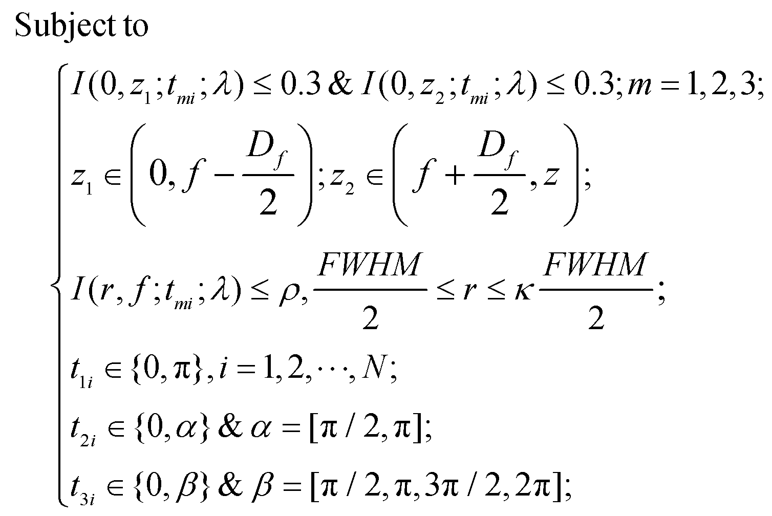
When the planar SOLs are normally illuminated by the monochromatic plane wave, the normal optical distribution after the lens surface is shown in Fig. 1a. The planar SOLs with different phase modulations are shown in Fig. 1b, in which we investigate three SOLs with successively increased phase levels. Three sets of phase levels, listed as 0, π; 0, π/2, π; and 0, π/2, π, 3π/2, 2π, are taken into consideration. For simplicity, these three SOLs are denoted as sample #1, #2, and #3 in the following discussion, respectively. To obtain a customized programming model for flexibly designing the MPM SOLs, we restrain the intensity I along two orthogonal directions, including the optical axis and transverse axes in every focal plane. The sidelobe intensity ratio ρ is defined as the intensity distribution ratio between the side lobe and the central spot. After evaluation, a sidelobe intensity ratio ρ of 0.3 is chosen in our design. Also, the sidelobe intensity ratio ρ can be tuned to other values according to the specific requirements, which has been validated feasibly in our recent publication.23 For the multi-objective and multi-constraint optimization problem (known as the Pareto-optimal problem), the genetic algorithm (GA) is particularly well-suited.37,38 Compared with other optimization algorithms, such as the particle swarm optimization (PSO) and simulated annealing (SA), GA is powerful enough to exhibit parallel and global searching ability. In other words, GA can simultaneously search a solution space in diverse regions, which makes it possible to find a different solution set for complex problems, while PSO always falls into the local optimal solution. Therefore, GA can be treated as the most effective heuristic approach to solve multi-objective and multi-constraint optimization issues. Hence, we employ the GA to design the MPM SOLs that implement the predefined axial-intensity modulation over a given region. Here, a general universal optimization model is built up as eqn (1) and (2):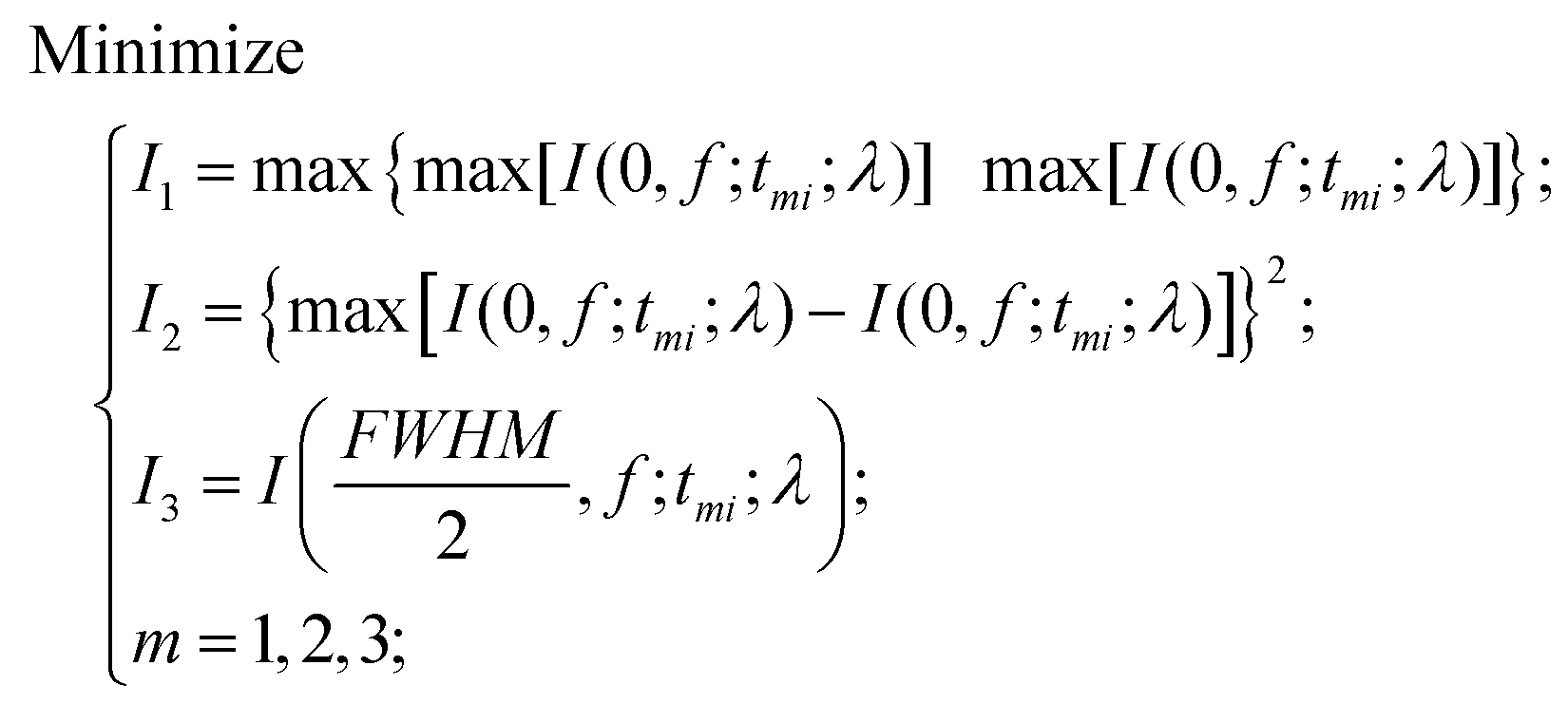 | (1) |
 | (2) |
 | ||
| Fig. 1 (a) Schematic illustration of sub-diffraction-limit focusing by SOLs; (b) Phase levels of the three SOLs. | ||
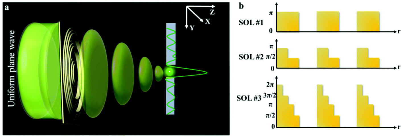
where I stands for the normalized electric-field intensity; tmi is the transmittance value of the i-th annular ring for the three samples and N is the total number of rings contained in the mask. The three objective functions are established to acquire a pre-determined peak axial intensity and focal plane distributions. To increase the focusing efficiency, the MPM mask distribution is introduced into the GA, in which the step-shaped phase distribution is generated by the specific constrained conditions. The detailed design procedures can be found in the ESI part I.† This unusual operation is applied on account of two important considerations: (i) the light is diffracted from the edges of the circles and focused into the central region through the constructive interference to enhance the focusing efficiency; (ii) the flexible operation can greatly simplify the lithography steps compared with the random multi-phase distribution. Hence, the major optimization steps are demonstrated in Fig. 2: First, create random phase masks as initial populations and calculate objective functions for different focal lengths and wavelengths, with each mask serving as the fitness value. Second, confine the random phase distribution to a step-shaped counterpart on the basis of several constraints added to the objective functions. Third, iteratively perform the genetic operations among the population (selection, crossover and mutation) and reinsert the offspring population to the original parental population according to the fitness value of each mask until the termination criterion is satisfied. Here, the sidelobe intensity ratio ρ along the radial axis is set to be below 0.3 to form a sharp contrast with the main hotspot, which helps to create favorable conditions during the fluorescence imaging process so that only the central hotspot can stimulate the fluorophores. The specific optimization process has been transformed and implemented through an unconstrained multi-objective GA based on vectorial angular spectrum (VAS) theory.26 The fast Hankel transformation is applied to accelerate the computational processes. In the end, the best structural mask in the population is achieved.
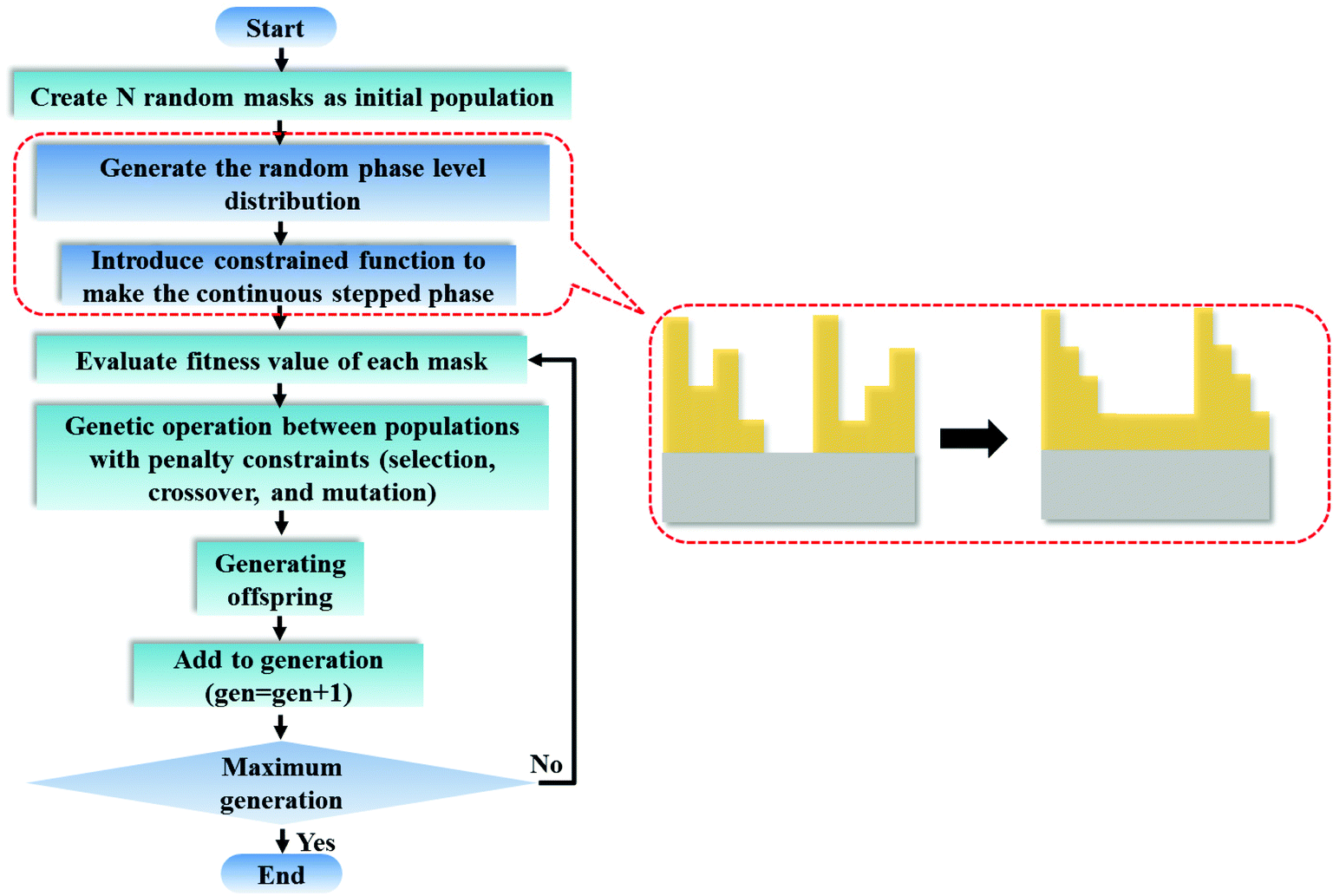 | ||
| Fig. 2 The optimization procedure for the MPM SOLs. | ||
The detailed optimization parameters of these three MPM SOLs are provided in the ESI.† What should also be mentioned here is that the diameters of the designed SOLs are all set to be as large as 2 mm to enhance their compatibility with the commercialized optical system. Meanwhile, all lenses have the same focal length, f0 = 2 mm, and the designed full width at half maximum (FWHM) of the hotspot is about 1.12λ, which is smaller than the Rayleigh criterion of 1.33λ. Moreover, the 5 μm smallest annular size of the designed SOLs makes it possible to fabricate a millimeter-scale device through a normal lithography process.
Note that the theoretical calculations via Matlab are performed without the consideration of the realistic thickness of the structure. To see the difference between the theoretical calculations and the results generated from the finite-difference time-domain (FDTD) method, we just give an example of the sample with R = 10 μm and the focal length f = 7 μm for the sake of computer resources. The comparisons are demonstrated in Fig. S2 (ESI),† and we can see that the VAS result exhibits a slight focal shift compared with the result of FDTD simulation. Nevertheless, the difference does not influence the estimation of the focal length of the designed SOLs. Fortunately, the hotspot sizes remain almost unchanged for the two results.
Wafer-level fabrication of MPM SOLs
We established a parallel fabrication flow for the MPM SOLs, as shown in Fig. 3. Fig. 4 presents device images of the fabricated three SOLs and scanning electron microscopy (SEM) images with the zoom-in view. Notably, the fabrication error generated by basic lithography can be controlled within ±0.2 μm, ensuring the focusing performance of SOLs without significant deviation from the design. The cross-sectional view of the as-fabricated SOLs’ geometrical profiles for the three samples marked radially by A′–A′, B′–B′, and C′–C′, respectively, is also depicted in Fig. 4b2, 4c2 and 4d2. From these pictures, we can obviously see that the reactive ion etching (RIE) process encountered a slight problem with sloped sidewalls,39–42 which can be attributed to the intrinsic isotropic chemical etching mechanism.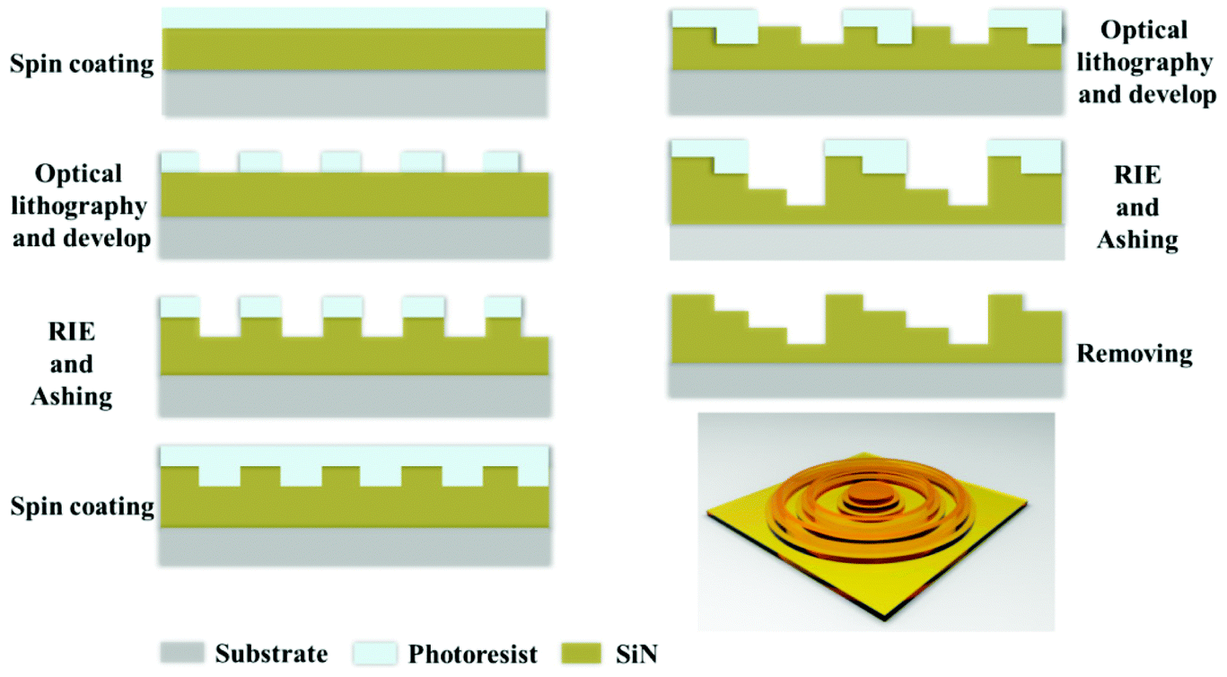 | ||
| Fig. 3 The 4-inch wafer-level fabrication flow for the step-shaped MPM SOLs. | ||
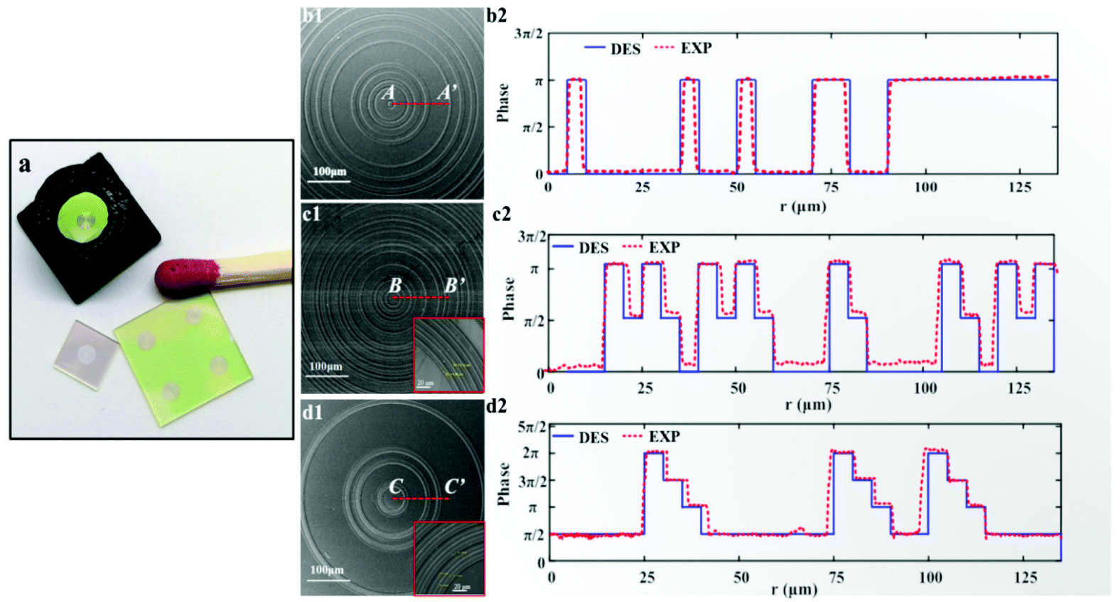 | ||
| Fig. 4 The device images obtained by both SEM and a step profiler for the three fabricated MPM SOLs. (a) The device image of the MPM SOLs; (b1, c1, d1) The SEM images for the three samples; (b2, c2, d2) The cross-sectional views of the as-fabricated SOLs' geometrical profiles radially for the three samples. | ||
Results and discussion
Experimental measurements of focusing performance
For experimental characterization, the transmitted light patterns are collected by a 100×/0.9 Nikon inverted microscope objective and a suitable high-resolution camera slice by slice with an axial step of 100 nm, as shown in Fig. S4 (ESI).† The computed axial intensity distributions of the three SOLs are depicted in Fig. 5a1, b1, and c1. Meanwhile, the practically measured axial light intensity distributions are demonstrated in Fig. 5a2, b2, and c2, and the fluctuant focal patterns that occurred can be attributed to the fabrication imperfections and the slight vibration of the environment.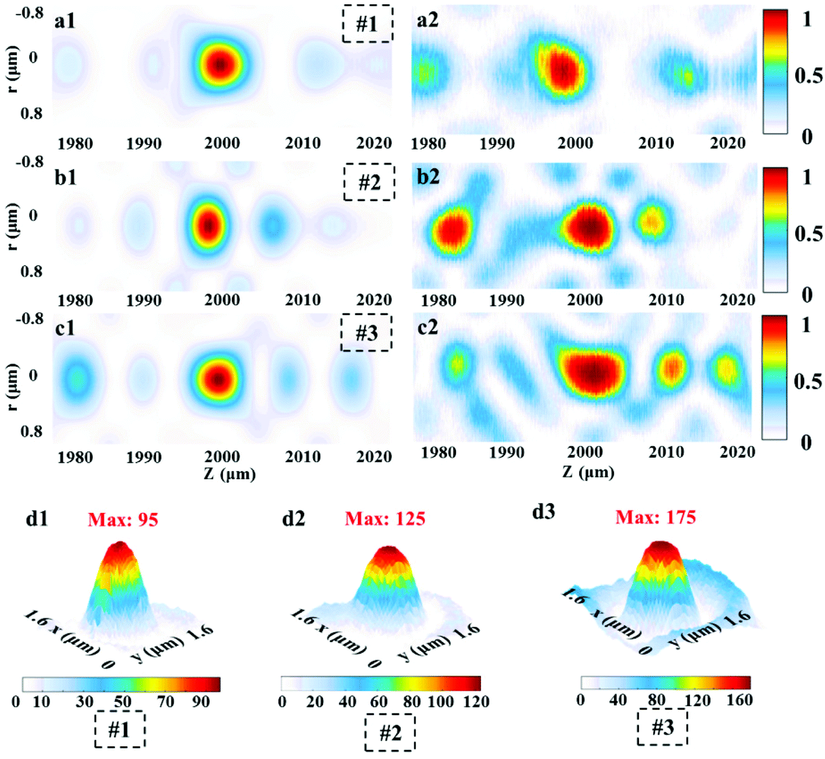 | ||
| Fig. 5 Simulated and experimental results of the MPM SOLs at 532 nm. (a1, b1, c1) Simulated and (a2, b2, c2) experimental light distributions in the X–Z cross-section; (d1, d2, d3) experimental results in the focal planes for the three samples. | ||
To validate the suggested approach, the simulated focusing efficiency of the MPM SOLs was calculated based on the FDTD method. Actually, we took three samples with the diameter of 20 μm into consideration for just the conceptual demonstration, as the millimeter-scale device simulation requires a huge computer resource (see Table S3 in the ESI†). The results show that the theoretical focusing efficiency can be improved as the phase levels increase. Moreover, the focusing efficiency for the multi-level SOL with a step-shaped phase is much higher than that of the MPM SOL with a random phase (see Table S3 in the ESI†). Then, the focusing intensities of the three samples were quantitatively characterized, and we just used the CCD camera to record the focusing intensity on the focal plane43 for the samples. What should be noted here is that to acquire more accurate results, the focusing intensity of the home-made pulsed laser and the integral time of the camera are kept unchanged throughout the whole measurement. Fig. 5d1–d3 show the focusing patterns, as well as the maximum intensity for each sample. The experimental results indicate that with the increased phase level, the focusing intensity is gradually enhanced, which agrees well with the simulations. Through efficiently manipulating the wavefronts, a stronger light concentration at the focal spot can be expected by further increasing the phase level.44,45
A shadow occurs for the grooves when the radiation originating from one zone of the SOLs must pass through another before reaching the focal spot. The incident light within the shadowing zones cannot be converged to the focal spot, which may influence the focusing efficiencies of the stepped SOLs. To see how the shadow effect impacts the focusing performance of the high NA structure, we designed 2-step SOLs with three different NAs; the focusing efficiencies of each sample are included in Table S2 in the ESI.† According to Table S2,† we note that the shadow effect can clearly affect the focusing efficiencies of high-NA stepped SOLs. The focusing efficiencies decrease with the increase of the NA, which can be attributed to the increased light scattering at larger diffraction angles.
To study the sidelobe intensity distribution in the focal plane, the intensity profiles along the radial axis are shown in Fig. 6. We can see that the sidelobe intensity ratios for the three samples are all well controlled below 0.3, which enhances the fluorescence contrast with the central focal region during the imaging process. The zoom-in views for each sample exhibit good agreement between the simulation and measurement. The computed hotspot sizes are 1.12λ at λ = 532 nm. Comparatively, the experimental hotspots for the three samples are (1.16 ± 0.02)λ, (1.21 ± 0.01)λ, and (1.22 ± 0.02)λ, respectively. The results are the average of three measurements. As expected, the simulated and experimental sizes are all beyond the calculated Rayleigh diffraction limit of 1.33λ. What should be noted here is that due to the restrictions of computer memory resources, we only calculated the main super-oscillatory hotpots from −0.8 μm to 0.8 μm. To see the actual intensity distribution in a much larger spatial range, we illustrate the experimental results in the region from −15 μm to 15 μm.
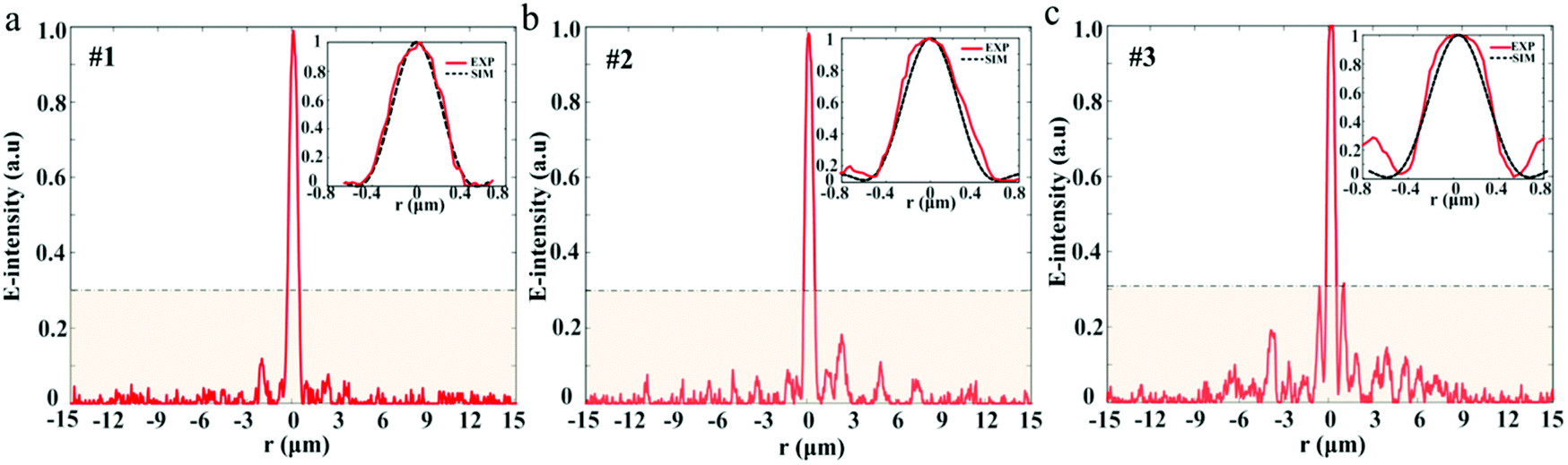 | ||
| Fig. 6 The experimental radial intensity distribution along the focal plane for the three samples are shown in (a), (b), and (c), respectively. Also, the corresponding zoom-in views showing the simulated and experimental results for the three samples are given in each subgraph. | ||
Imaging of fluorescent particles
Compared with the high-energy optical damage generated by STED, PALM and STORM, the focusing intensity actually needed in biological fluorescence microscopy is rather moderate but enough to stimulate the fluorophores. Thanks to the delicate interference of the far-field propagating waves, only a little part of the incident light is focused at the central spot. The SOL can then be treated as an energy attenuator to efficiently alleviate the problems such as strong photobleaching and phototoxicity. Nevertheless, the actual focusing efficiency of SOLs is always disappointing when truly used in super-resolution fluorescence microscopy. We established a customized microscope system working in step-by-step scanning mode in the x–y plane based on the MPM SOL. Here, SOL #3 is selected as the imaging device for its highest focusing intensity among the three fabricated lenses. Note that the size of the fluorescent particles of 2 μm-diameter (excitation wavelength is 540 nm and the emission wavelength is 580 nm) is too large for direct observation; we just distinguished the intervals between the particles to inspect the resolving power of the imaging system. The excitation and emission spectra of the fluorescent particles are shown in Fig. S5.† A schematic diagram of the whole imaging equipment can be seen in Fig. 7a and the detailed imaging parameters can be found in the ESI.† Since there is an inherent contradiction between the high NA and long working distance, the imaging samples are always restrained near the lens surface. As a matter of fact, this SOL-based microscopy exhibits an ultralong working distance of 2 mm, an almost two-order improvement,18 providing sufficient space for sample adjustment. The fluorescent particles dispersed on the glass slide are placed at the focal region of the SOL and scanned in the x–y plane during the imaging process. Owing to the unique advantage of the arbitrarily controlled light-field patterns of the SOLs, the sidelobe intensity can be tuned to impossibly lighten the fluorescent particles, but the fluorophores under the illumination of the focal spot can be activated. Fig. 7b shows a schematic diagram of the imaging principle. This flexible design removes the pinhole, which apparently simplifies the whole imaging setup compared to the work in ref. 11 and 18. Finally, the three dispersive fluorescent particles are lightened successively, and the sample contour is reconstructed via imaging fusion, as shown in Fig. 7c.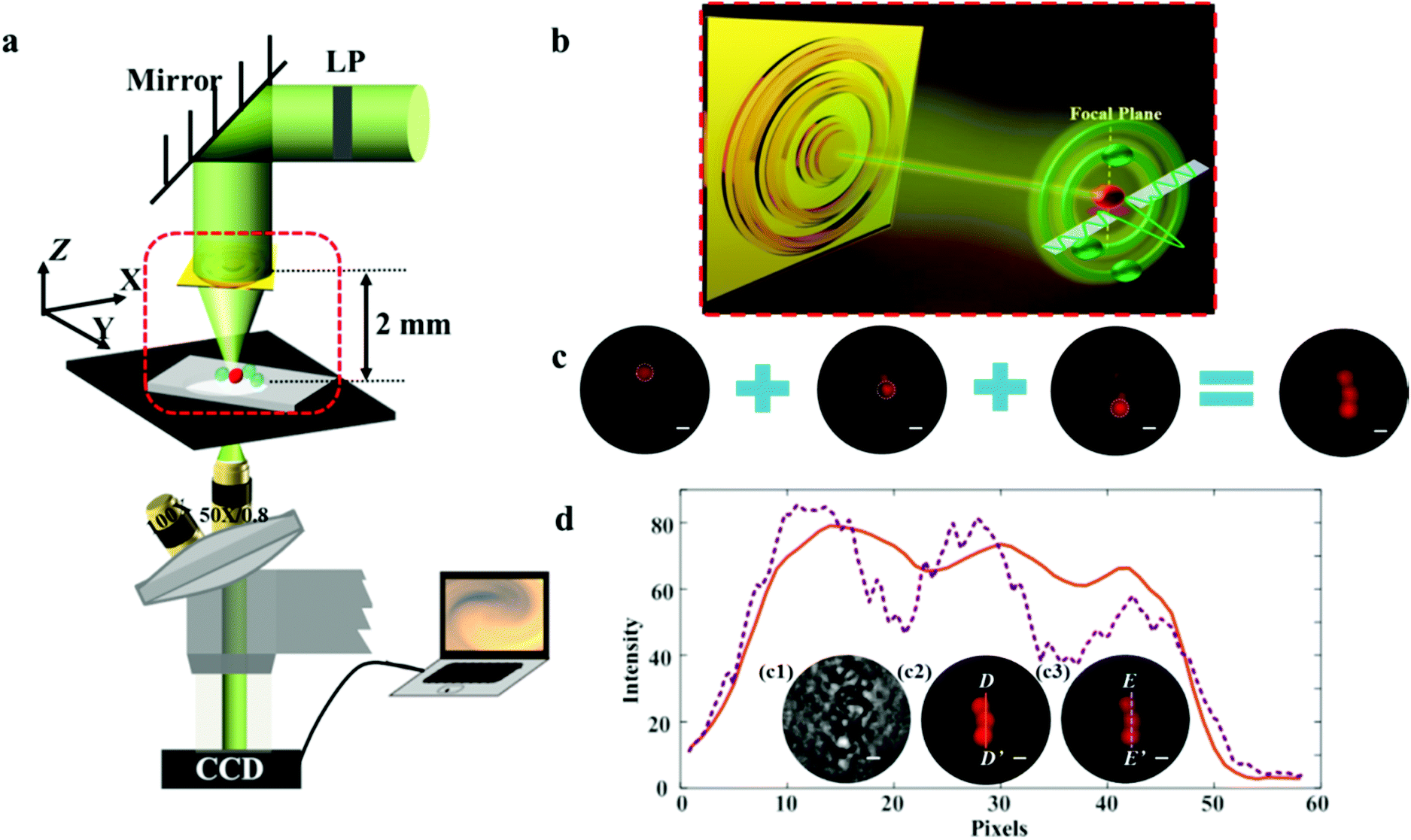 | ||
| Fig. 7 (a) Schematic of imaging measurement setup for the dispersive fluorescent particles. LP: Linear Polarizer. (b) Illustrative diagram for imaging the fluorescent particles. (c) Superposition operation of the achieved images. (d) The imaging results of fluorescent nanoparticles obtained by employing bright-field microscopy, wide-field fluorescence microscopy and SOL-based microscopy, respectively. Scale bar, 1 μm. | ||
Fig. 7d1 depicts the imaging results for the transparent dispersive samples directly exposed to the bright field, from which we can see that the contour of the sample seems blurred and the fluorescent particles cannot be identified clearly, which makes it difficult to depict the line profile under the bright-field condition. Compared with the results captured using wide-field fluorescence microscopy (Fig. 7d2), the morphology of the dispersive samples can be more clearly distinguished utilizing the super-resolution point light source (Fig. 7d3). The light intensity distribution along the line D–D′ and E–E′ is also depicted in Fig. 7d. From the rough contour profile mapped using wide-field fluorescence microscopy employing the 50×/0.8 objective, we can see that the fine details between the samples are missing. In contrast, the imaging results of our SOL-based fluorescence microscopy system can clearly distinguish the sophisticated details of the samples, with the resolving power of about 1.07λ, beating the diffraction limit of 1.33λ. A shorter-wavelength light source can be used to further improve the resolving power of the imaging system.
Conclusions and outlook
SOL-based optical microscopy is a highly customized, non-invasive and universal imaging technique without complex mathematical post-processing. Actually, only a little part of the incident light is focused into the central spot while the other energy is turned into high-intensity sidelobes. Note that the definition of the SCL lens has been put forward in the literature,14,18,19 and we can see that there is a tradeoff between the sub-diffraction spot size and the sidelobe intensity. To find solutions for the challenges of sidelobe suppression and focusing efficiency enhancement from the perspective of structure innovation and algorithm improvement, we have proposed a MPM method to improve the focusing efficiency and reduce the sidelobes of the present BP-type SOLs. Three SOLs with increased phase levels are optimized. The proposed MPM SOL with the step-shaped phase distribution can also reduce the fabrication complexity compared with the present multi-level structures, potentially for wafer-level fabrication of a large-scale lens. As expected, the focal spots for the three samples are all beyond the Rayleigh diffraction limit without significant sidelobes. And the focal intensities of the samples with multiple phase levels are experimentally validated. Different from the natural results of sidelobe suppression and efficiency enhancement generated from the supercritical lens (SCLs), two distinctions should be noted here: (1) we applied a flexible design method to control the intensity concentration ratio in the focal plane to fulfil the customized optical contours; (2) the focusing efficiency of the SOLs is efficiently improved through the MPM method. For phase-type SOLs, multiple phase levels instead of the binary phase would be beneficial to reduce the side lobes and increase the focusing efficiency. The optical performance of the MPM SOLs is enhanced through efficient manipulation of the wavefronts, and a stronger light concentration at the focal spot is achieved as the phase levels increase.Then, we established the SOL-based optical fluorescence microscopy to verify its practical imaging capacity. The distance between the fluorescent particles can be much distinctly mapped compared with the results achieved by wide-field fluorescence microscopy, which encouragingly beat the Rayleigh diffraction limit. The sidelobe intensity can be tuned to impossibly lighten the fluorescent particles, and the fluorophores under the illumination of the SOL can be activated to avoid unwanted excitation. Hence, the whole imaging system can be efficiently simplified free from the pinhole filter. Additionally, the energy ratio for the focusing hotspot of the SOL can be further elaborately adjusted to satisfy various samples without damaging the biological activity, which greatly helps to build up the customized optical imaging system. Compared with the conventional imaging lenses, the SOL-based microscopy exhibits an ultralong millimeter-scale working distance of about 2 mm, providing sufficient space for sample adjustment. The developed imaging process is purely physical, and it does not need any pre-processing of the samples or mathematical post-processing of the imaging results. Admittedly, the current SOL-based microscopy system is constructed by a step-by-step scanning mode, and the imaging speed is mainly restricted by the rather long response time of the piezo stage and low performance of the data acquisition (DAQ) card. We believe that the imaging speed can be further increased through changing the piezo stage into a continuous scanning mode via programming development and the replacement with a higher-performance DAQ device. In the future, the resolving power of the imaging system can be further enhanced to sub-100 nm by using a shorter wavelength for illumination and a more optimized MPM structural mask for the SOL. By utilizing the proposed design strategy in our previous research,26 micrometer-scale ring components are necessary to construct the entire SOL, making the low-cost, yet wafer-level fabrication feasible for potential applications.
The proposed idea provides a methodological solution to improve the focusing efficiency of SOLs. The efficiency-enhanced and sidelobe-suppressed SOLs can efficiently promote practical applications for the planar SOLs in many fields, such as non-invasive biomedical imaging, laser tweezing, optical coherence tomography imaging, aerospace photonics, lab-on-a-chip devices and micro/nanofabrication. And the unique advantage of the customized light-field patterns for the SOLs in the far-field will make biological imaging much more flexible and efficient.
Experimental section
First, a SixNy layer is deposited on a 4-inch pyrex glass substrate by plasma-enhanced chemical vapor deposition (PECVD), followed by the normal lithography process. Then, RIE is progressed to form the desired non-subwavelength SixNy ring belts. Based on the previously optimized phase distribution, more than one lithography steps are needed. The optical path delay for a thickness, t, is Δ = (n − 1)t, which corresponds to a phase shift of Δ/λ × 2π, where n is the refractive index of the material and λ is the wavelength of light. To achieve a phase shift of 2π, t must be at least λ/(n – 1) ∼ 0.8λ. As shown in the ESI,† the measured refractive index of the SixNy layer was about 2.25 at the wavelength of 532 nm, and the thickness of each layer for the SixNy ring belts was fabricated on the basis of the optimized phase difference. The total thickness of the SixNy layer for SOL #1 and SOL #2 is 212 nm, and it is 424 nm for SOL #3 for their different total phase difference π and 2π, respectively.Conflicts of interest
There are no conflicts to declare.Acknowledgements
We acknowledge the financial support from the Science, Technology and Innovation Commission of Shenzhen Municipality (JCYJ20180508151936092), the National Natural Science Foundation of China (51975483), the Fundamental Research Funds for the Central Universities (31020190504001), the 111 Project (B13044), and the Innovation Foundation for Doctor Dissertation of Northwestern Polytechnical University (CX201908). We would also like to thank the Analytical & Testing Center of Northwestern Polytechnical University for the fabrication and characterization of SOL samples.References
- C. Lu, W. Tang, Y. Liu, S. Chang, F. Wu, C. Chen, Y. Tsai, S. Yang, C. Kuo, Y. Okada, Y. Hwu, P. Chen and B. Chen, Commun. Biol., 2019, 2, 177 CrossRef PubMed.
- B. Giepmans, S. Adams, M. Ellisman and R. Tsien, Science, 2006, 312, 217–224 CrossRef CAS PubMed.
- M. Heilemann, S. Van De Linde, M. Schüttpelz, R. Kasper, B. Seefeldt, A. Mukherjee, P. Tinnefeld and M. Sauer, Angew. Chem., Int. Ed., 2008, 47, 6172–6176 CrossRef CAS PubMed.
- A. Dilipkumar, A. Al-Shemmary, L. Kreiß, K. Cvecek, B. Carle, F. Knieling, J. Menezes, O. Thaoma, M. Schmidt, M. Neurath, M. Waldner, O. Friedrich and S. Schurmann, Adv. Sci., 2019, 6, 1801735 CrossRef PubMed.
- S. Hell and J. Wichmann, Opt. Lett., 1994, 19, 780–782 CrossRef CAS PubMed.
- M. Gustafsson, J. Microsc., 2000, 198, 82–87 CrossRef CAS PubMed.
- E. Betzig, G. Patterson, R. Sougrat, O. Lindwasser, S. Olenych and J. Bonifacino, Science, 2006, 313, 1642–1645 CrossRef CAS PubMed.
- B. Huang, S. Jones, B. Brandenburg and X. Zhuang, Nat. Methods, 2008, 5, 1047 CrossRef CAS PubMed.
- X. Dong, A. Wong, M. Kim and G. Eleftheriades, Optica, 2017, 4, 1126–1133 CrossRef.
- Y. Kozawa, D. Matsunaga and S. Sato, Optica, 2018, 5, 86–92 CrossRef CAS.
- E. T. F. Rogers, J. Lindberg, T. Roy, S. Savo, J. Chad, M. Dennis and N. I. Zheludev, Nat. Mater., 2012, 11, 432–435 CrossRef CAS PubMed.
- R. Remez, Y. Tsur, P. Lu, A. Tavabi, R. Dunin-Borkowski and A. Arie, Phys. Rev. A, 2017, 95, 031802 CrossRef.
- Y. Eliezer and A. Bahabad, Optica, 2017, 4, 440–446 CrossRef.
- K. Huang, H. Ye, J. Teng, S. P. Yeo, B. Luk'yanchuk and C. W. Qiu, Laser Photonics Rev., 2014, 8, 152–157 CrossRef CAS.
- Y. Shen, Y. Peng, F. Cai, K. Huang, D. Zhao, C. Qiu, H. Zheng and X. Zhu, Nat. Commun., 2019, 10, 3411 CrossRef PubMed.
- K. Huang, F. Qin, H. Liu, H. Ye, C. Qiu, M. Hong, B. Luk'yanchuk and J. Teng, Adv. Mater., 2018, 30, 1704556 CrossRef PubMed.
- Y. Eliezer and A. Bahabad, ACS Photonics, 2016, 3, 1053–1059 CrossRef CAS.
- F. Qin, K. Huang, J. Wu, J. Teng, C. W. Qiu and M. Hong, Adv. Mater., 2017, 29, 1602721 CrossRef PubMed.
- C. Hao, Z. Nie, H. Ye, H. Li, Y. Luo, R. Feng, X. Yu, F. Wen, Y. Zhang, C. Yu, J. Teng, B. Luk'yanchuk and C. W. Qiu, Sci. Adv., 2017, 3, e1701398 CrossRef PubMed.
- F. Zanacchi, Z. Lavagnino, M. Faretta, L. Furia and A. Diaspro, PLoS One, 2013, 8, e67667 CrossRef PubMed.
- B. Schmid, G. Shah, N. Scherf, M. Weber, K. Thierbach, C. Campos, I. Roeder, P. Aanstad and J. Huisken, Nat. Commun., 2013, 4, 2207 CrossRef PubMed.
- J. S. Diao, W. Z. Yuan, Y. T. Yu, Y. C. Zhu and Y. Wu, Opt. Express, 2016, 24, 1924–1933 CrossRef PubMed.
- M. Y. Li, W. L. Li, H. Y. Li, Y. C. Zhu and Y. T. Yu, Sci. Rep., 2017, 7, 01335 CrossRef PubMed.
- Y. Yu, W. Li, H. Li, M. Li and W. Yuan, Nanomaterials, 2018, 8, 185 CrossRef PubMed.
- W. Li, Y. Yu and W. Yuan, Nanoscale, 2019, 11, 311–320 RSC.
- G. H. Yuan, E. T. F. Rogers and N. I. Zheludev, Light: Sci. Appl., 2017, 6, e17036 CrossRef CAS PubMed.
- Q. Wang, J. Maddock, E. T. F. Rogers, T. Roy, C. Craig, K. F. Macdonald, D. W. Hewak and N. I. Zheludev, Appl. Phys. Lett., 2014, 104, 121105 CrossRef.
- G. Yuan, E. T. F. Rogers, T. Roy, G. Adamo, Z. Shen and N. I. Zheludev, Sci. Rep., 2014, 4, 06333 CrossRef CAS PubMed.
- K. S. Rogers, K. N. Bourdakos, G. H. Yuan, S. Mahajan and E. T. F. Rogers, Opt. Express, 2018, 26, 8095–8112 CrossRef PubMed.
- H. Ni, G. Yuan, L. Sun, N. Chang, D. Zhang, R. Chen, L. Jiang, H. Chen, Z. Gu and X. Zhao, RSC Adv., 2018, 8, 20117–20123 RSC.
- G. Cao, H. Lin, S. Fraser, X. Zheng, B. D. Rosal, Z. Gan, S. Wei, X. Gan and B. Jia, ACS Appl. Mater. Interfaces, 2019, 11, 20298–20303 CrossRef CAS PubMed.
- Z. Wen, Y. He, Y. Li, L. Chen and G. S. Chen, Opt. Express, 2014, 22, 22163–22171 CrossRef PubMed.
- D. Tang, C. Wang, Z. Zhao, Y. Wang, M. Pu, X. Li, P. Gao and X. Luo, Laser Photonics Rev., 2015, 9, 713–719 CrossRef CAS.
- G. Yuan, S. Vezzoli, C. Altuzarra, E. T. F. Rogers, C. Couteau, C. Soci and N. I. Zheludev, Light: Sci. Appl., 2016, 5, e16127 CrossRef CAS PubMed.
- J. Wu, Z. Wu, Y. He, A. Yu, Z. Zhang, Z. Wen and G. Chen, Opt. Express, 2017, 25, 6274–6282 CrossRef PubMed.
- D. Tang, L. Chen and J. Liu, Opt. Express, 2019, 27, 12308–12316 CrossRef CAS PubMed.
- A. Konak, D. W. Coit and A. E. Smith, Reliab. Eng. Syst. Safety, 2006, 91, 992–1007 CrossRef.
- C. M. Fonseca and P. J. Fleming, IEEE Trans. Syst. Man Cybern. A: Syst. Hum., 1998, 28, 38–47 CrossRef.
- Z. Zhang, C. Guo, R. Wang, H. Hu, X. Zhou, T. Liu, D. Xue, X. Zhang, F. Zhang and X. Zhang, Opt. Express, 2017, 25, 33676–33687 CrossRef CAS.
- S. Doshay, D. Sell, J. Yang, R. Yang and J. A. Fan, APL Photonics, 2018, 3, 011302 CrossRef.
- A. M. Shaltout, J. Kim, A. Boltasseva, V. M. Shalaev and A. V. Kildishev, Nat. Commun., 2018, 9, 2673 CrossRef PubMed.
- H. C. Wang, C. H. Chu, P. C. Wu, H. H. Hsiao, H. J. Wu, J. W. Chen, W. H. Lee, Y. C. Lai, Y. W. Huang, M. L. Tseng, S. W. Chang and D. P. Tsai, Small, 2018, 14, 1703920 CrossRef PubMed.
- X. Zheng, B. Jia, H. Lin, L. Qiu, D. Li and M. Gu, Nat. Commun., 2015, 6, 8433 CrossRef CAS PubMed.
- E. Di Fabrizio, F. Romanato, M. Gentili, S. Cabrini, B. Kaulich, J. Susini and R. Barrett, Nature, 1999, 401, 895–898 CrossRef CAS.
- G. Chen, Z. Q. Wen and C. W. Qiu, Light: Sci. Appl., 2019, 8, 1–23 CrossRef CAS PubMed.
Footnote |
| † Electronic supplementary information (ESI) available: Details of design parameters, comparison and influence analysis, optical measurement, and simulated focusing efficiency. See DOI: 10.1039/c9nr10697a |
| This journal is © The Royal Society of Chemistry 2020 |