
 Open Access Article
 This Open Access Article is licensed under a
 Creative Commons Attribution 3.0 Unported Licence
Minimally invasive spin sensing with scanning tunneling microscopy†
Luigi
Malavolti
 *abc,
Gregory
McMurtrie
abc,
Steffen
Rolf-Pissarczyk
bc,
Shichao
Yan
bcd,
Jacob A. J.
Burgess
bce and
Sebastian
Loth
*abc
*abc,
Gregory
McMurtrie
abc,
Steffen
Rolf-Pissarczyk
bc,
Shichao
Yan
bcd,
Jacob A. J.
Burgess
bce and
Sebastian
Loth
*abc
aInstitute for Functional Matter and Quantum Technologies, University of Stuttgart, 70569 Stuttgart, Germany. E-mail: sebastian.loth@fmq.uni-stuttgart.de; luigi.malavolti@fmq.uni-stuttgart.de
bMax Planck Institute for the Structure and Dynamics of Matter, 22761 Hamburg, Germany
cMax Planck Institute for Solid State Research, 70569 Stuttgart, Germany
dSchool of Physical Science and Technology, ShanghaiTech University, Shanghai 201210, China
eDepartment of Physics and Astronomy, University of Manitoba, Winnipeg, Manitoba, Canada R3T 2N2
First published on 21st May 2020
Abstract
Minimizing the invasiveness of scanning tunneling measurements is paramount for observation of the magnetic properties of unperturbed atomic-scale objects. We show that the invasiveness of STM inspection on few-atom spin systems can be drastically reduced by means of a remote detection scheme, which makes use of a sensor spin weakly coupled to the sensed object. By comparing direct and remote measurements we identify the relevant perturbations caused by the local probe. For direct inspection we find that tunneling electrons strongly perturb the investigated object even for currents as low as 3 pA. Electrons injected into the sensor spin induce perturbations with much reduced probability. The sensing scheme uses standard differential conductance measurements, and is decoupled both by its non-local nature, and by dynamic decoupling due to the significantly different time scales at which the sensor and sensed object evolve. The latter makes it possible to effectively remove static interactions between the sensed object and the spin sensor while still allowing the spin sensing. In this way we achieve measurements with a reduction in perturbative effects of up to 100 times relative to direct scanning tunneling measurements, which enables minimally invasive measurements of a few-atom magnet's fragile spin states with STM.
The process of measuring an object can impact its state. This often unwanted effect, also called the observer effect, is striking for quantum phenomena1,2 and remarkably important for the investigation of atomic scale objects. In particular, the magnetic stability of atomic-scale magnets is extremely sensitive to small variations in their local environment,3,4 whether intrinsic or measurement induced.5,6 Minimizing the invasiveness of the measurement process is critical for the observation of unperturbed atomic-scale magnets. This has to be taken into special consideration when trying to harness their magnetic states for data storage,7,8 spintronics8 and quantum devices.8–10
Scanning probe microscopy has become an essential tool11 for probing magnetic surfaces,12–14 atoms,4,15–18 atom chains,19,20 and molecules.21–28 All scanning probe techniques – irrespective of whether they use magnetic forces or spin-polarized current for detection – require the presence of a local probe tip. Its proximity can perturb the investigated object, through mechanical interaction,29–32 magnetic stray field,33 electric fields,23,29,34–37 magnetic exchange coupling12,14,38 as well as electron injection.7,39 Whereas magnetic force and magnetic exchange force microscopy have been used to great effect for the investigation of extended magnetic surfaces without the use of electric current, the majority of atomic-scale magnetic structures have been studied with STM where the impact of the tunneling electrons must be considered.
Here, we demonstrate that the invasiveness of direct STM inspection can be minimized and quantified via a remote detection scheme using a spin sensor. This remote detection scheme is inspired by optical quantum non-demolition measurements2 and a recent report where ESR-STM was used to detect the state of a nearby magnetic atom.40 An indirect observation of the object's spin state is performed by measuring a nearby sensor spin weakly coupled to the sensed object. This substantially reduces the perturbation induced by the STM measurements, while also allowing the perturbation to be identified by comparison with direct inspection data.
We demonstrate that by using a kinked chain of three iron atoms as a sensor spin, minimally invasive measurements of a nearby eight-atom nano-antiferromagnet (nano-AF) can be performed. The nano-AF was chosen because transitions between its Néel-like ground states are determined by magnetic tunneling and variations of the switching rate are a direct measure for the invasiveness of the sensing scheme. In the scope of this work, intrinsic switching rates refer to the time evolution of the isolated spin system on a surface in absence of probe induced perturbations. In particular, we show a possible route to minimize the perturbation induced by STM investigation, shedding light on the many different aspects that one must take into account when designing minimally invasive measurements.
We find the tunneling current is the main perturbation for direct STM inspection, even for tunneling currents as low as 3 pA. The remote sensing scheme, explicitly avoiding direct tunneling, is 100 times less perturbative. To reach this level of isolation, we show that the sensing scheme must rely on spin states of the sensor spin mismatched to those of the sensed object. Furthermore, to effectively cancel the sensor-nano-AF interaction a dynamic decoupling scheme is employed by making use of the rapid switching of the sensor's magnetic states during the measurement. This approach effectively allows the primary STM induced perturbations of the magnetic dynamics of the nano-AF to be suppressed, and, by comparison with direct inspection data, identified. As such, our report establishes a general method of tailoring the sensing scheme to mitigate STM induced perturbations.
Both the sensor spin and the nano-AF were assembled with Fe atoms on a monatomic layer of Cu2N grown on Cu(100), Fig. 1a. Fe atoms on Cu2N have a spin of magnitude 2 and exhibit large easy-axis magnetocrystalline anisotropy (z direction, Fig. 1b) with a small transverse anisotropy contribution.41,42 The Cu2N surface mediates long-range magnetic interaction through π and σ states of the Cu–N network, allowing remote spin sensing via weak μeV-scale interaction between nano-AFs.43
 | ||
| Fig. 1 Direct and remote measurement of the nano-AF's switching. (a) Spin-polarized STM image of the nano-AF in spin state ‘0’ (left structure consisting of 8 Fe atoms) and the spin sensor (right structure consisting of 3 Fe atoms). The distance between the nano-AF and the sensor is 1.9 nm; tunnel junction setpoint 4 mV, 5 pA. (b) Same area as (a) with the nano-AF in state ‘1’. Arrows labeled x, y, z show the reference coordinate system. (c) dI/dV(V) spectra acquired with the tip positioned over the sensor (blue star in (b)) when the nano-AF is in state ‘0’ (red line) or ‘1’ (blue line). Inset shows the zoom of the pronounced dip at −5.4 mV bias voltage highlighting the (dI/dV)dip used for the sensing scheme. (d) Time trace of the tip position, Y, with the spin-polarized tip over the nano-AF (green star in (b)). STM feedback loop set to maintain constant current 2 pA at −3 mV bias. (e) Time trace of the (dI/dV)dip signal recorded with the tip over the sensor (blue star in (b)). STM feedback loop set to maintain constant current 150 pA at −5.2 mV bias. AC bias modulation for dI/dV(V) detection is 720 μV. Two-state switching of the nearby nano-AF appears as jumps in (dI/dV)dip at much reduced rate compared to (d) despite 50-fold increased tunnel current. (f) Correlation plot between the nano-AF state observed with the tip over the nano-AF and (dI/dV)dip obtained by measurement on the sensor. (g) Schematic representation of the Fe atom sensor on the Cu2N surface showing surface Cu atoms (dark blue), N atoms (light blue), Fe atoms (green). Arrows on Fe atoms indicate the magnetic moment orientation in the external magnetic field. All measurements were acquired at 2 T magnetic field along the Z direction. | ||
The nano-AF consists of two parallel rows of four Fe atoms each.7 In this arrangement the iron atoms couple antiferromagnetically; the nano-AF features two stable Néel-like ground states (labelled state '0' and state '1') and is insensitive to external magnetic fields.7 We therefore consider the effect, if any, of the external magnetic field to be part of the nano-AF environment. A spin-polarized tip was prepared by functionalizing the apex with Fe atoms picked up from the surface. The external magnetic field (see Fig. 1g) determines the direction of the tip polarization.44 Topographic imaging with a spin-polarized tip resolves these two states as a checkerboard-pattern in the apparent height of the constituent Fe atoms, Fig. 1a and b. At low temperature (0.5 K), the spontaneous switching of the nano-AF between the two Néel-like states is sufficiently slow to be detected by conventional STM measurements. Time traces of this switching can be recorded by monitoring the variations in apparent height of any atom of the nano-AF, Fig. 1d. This direct measurement on the nano-AF gives an average time between switching events in the tens of seconds.45
The sensor is comprised of three iron atoms arranged in a kinked chain, Fig. 1g. In this configuration the middle atom couples antiferromagnetically to the first and ferromagnetically to the third, as confirmed by spin-resolved topographies Fig. 1a, b and 2a. This geometry was selected because of its long spin relaxation time (2.8 μs in 2 T magnetic field, ESI S1†), as well as the strong dependence of its dI/dV(V) spectra on the external magnetic field, Fig. 2b. In particular, when measuring spectra with a spin-polarized tip and a 2 T field along the Fe's magnetic easy axis, the main features are due to spin excitations between short- and long-lived spin states.
 | ||
| Fig. 2 Characterization of the nano-AF and the sensor spin. (a) Spin-polarized STM image of the spin sensor. Tunnel junction setpoint 4 mV, 5 pA. (b) dI/dV(V) spectra acquired with a spin-polarized tip positioned over the top (red lines), second (green lines) and third Fe atom (blue lines). Tip positions are indicated in (a) as red, green and blue stars. Light colored spectra were measured at 0.75 T magnetic field and dark colored spectra at 2 T. (c) Plot of the spin state energies of the sensor as a function of magnetic field. The two low-energy states |+2, −2, −2〉 and |−2, +2, +2〉 are highlighted in light blue and orange. Spin states relevant to the dI/dV(V) features are highlighted in blue red and green color. (d) Spin-polarized STM image of the nano-AF. Tunnel junction setpoint 4 mV, 5 pA. (e) dI/dV(V) spectra acquired with a non-spin-polarized tip positioned over a peripheral (blue line) and central Fe atom (red line) of the nano-AF at 2 T magnetic field. Tip positions are indicated in (d) as blue and red stars. (f) Plot of the spin state energies of the nano-AF as function of magnetic field. The two degenerate ground states ‘0’ and ‘1’ are highlighted in orange and light blue. The spin states relevant to the spin excitations observed in (e) are highlighted with blue and red. Note that the two spin excitations at <6.5 meV have negligible transition intensities out of the ground state doublet. | ||
We find that dI/dV(V) spectra acquired over the third atom of the sensor show a significant signal variation, depending on the nano-AF state. This is most prominent at the minimum (dip) at −5.4 mV bias, Fig. 1c. The correlation between the two nano-AF Néel-like states and the high and low conductivity states of the sensor spin is reported in Fig. 1f. This was verified by rapidly moving the tip between the nano-AF and the sensor spin (see details in ESI S2†); hence, the time evolution of the signal at −5.4 mV, denoted (dI/dV)dip, remotely monitors the nano-AF switching, Fig. 1e. It is worth noting that the switching rate measured by remote sensing is an order of magnitude slower than that measured by direct inspection, an indication that direct inspection with the tip on the nano-AF is strongly perturbative in comparison with remote sensing.
To quantify how effective the remote conductance-based sensing mechanism is, we analyzed the signal-to-noise ratio (S/N) (see ESI S3 and S4†) as a function of bias voltage and tunnel current setpoints. The bias voltage dependence shows that the sensor is capable of detecting the nano-AF switching in 1 mV windows centered at positive and negative 5.2 mV bias. The best performance, a S/N of 8, is observed at −5.2 mV, Fig. 3a. The dependence of the S/N on tunnel current magnitude was evaluated at this voltage. It increases rapidly as the current setpoint is raised from 100 pA to 750 pA, where a maximum is reached, and then decreases slightly for higher currents, Fig. 3b. The noise magnitude in the sensor measurement depends linearly on the current (as experimentally confirmed, see ESI S4†). Since the current dependence of the signal to noise ratio shows a non-monotonic behavior, the measured signal must have a non-linear response. This points to a non-trivial role of the electron tunneling rate in the sensing signal, as confirmed by the model discussed below, which shows that the (dI/dV)dip signal is of dynamic origin.45
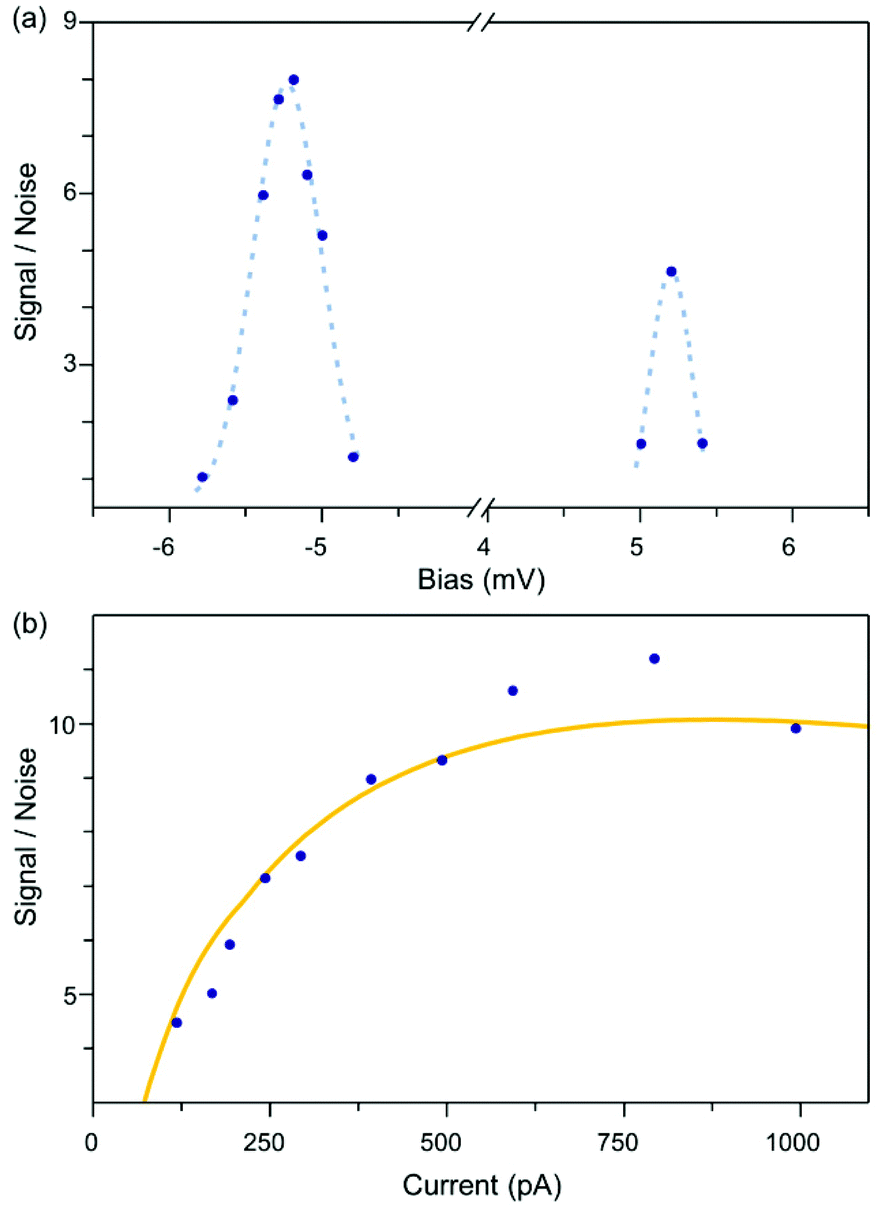 | ||
| Fig. 3 Signal to noise analysis of the sensing scheme performance. (a) Signal-to-noise ratio for remote measurement of the nano-AF spin states as a function of applied DC bias. Tunnel current setpoint 300 pA. Blue dots are experimental data, the dotted lines are guides to the eye. (b) Signal-to-noise ratio as function of tunnel current setpoint with an applied DC bias −5.2 mV. Blue dots are experimental data, orange line is a fit obtained using our model (see ESI† for details). | ||
We then use a rate equation model,45 which accounts for electron–spin scattering, to analyze the sensing scheme. It accurately reproduces the position and magnitude of all spectral features in the sensor's dI/dV(V) (see ESI S5†). The tunneling process responsible for the (dI/dV)dip signal variation is identified as inelastic tunneling that excites the sensor's spin from its ground state |+2, −2, −2〉 to the excited state |+2, −2, −1〉 (+2, −2, and −1 are the Sz expectation values of atom 1, 2, and 3, respectively, with z parallel to the external magnetic field). This is corroborated by the shift of the dip when changing the external magnetic field, Fig. 2b, in agreement with the Zeeman shift of the states, Fig. 2c.
Notably, the rate equation model indicates that the elaborate shape of the spectra is due to spin pumping effects.44,45 This dynamic process takes place when electron tunneling events occur on a time scale shorter than the sensor spin relaxation time. In the sensor, this is achieved via the long-lived metastable state |−2, +2, +2〉. Pump probe measurements46 determine its average lifetime to be 2.8 μs, and confirm the presence of the spin pumping mechanism (see ESI S1†). The (dI/dV)dip signal is therefore the consequence of averaging the conductance signals of different spin states; each state's contribution depends on its average population in dynamic equilibrium.45
Use of a non-local sensor avoids direct tunneling through the nano-AF, however, hot electrons generated in the tunneling processes may still propagate from the sensor to the nano-AF. This effect has been reported to trigger chemical reactions at tens of nanometers distance.47 To mitigate this effect, the sensor spin was designed to have the spin excitation, responsible for the (dI/dV)dip signal, at 5.2 meV. This is at a lower energy than the allowed nano-AF spin excitations at 6.5 meV and 8.4 meV (Fig. 2e and f). As such, the energy of electrons injected at the sensor with −5.2 mV bias is insufficient to trigger a spin excitation in the nano-AF. Further measurements using spin pumping features on the other atoms of the spin sensor indicate that slow switching rates can only be observed for voltages below the spin excitation threshold of the nano-AF. Our model indicates a clear correlation between the nano-AF's spin state and additional spin pumping features on the first and second atoms of the spin sensor. For sensor spin features above threshold, such as those at −7.2 mV on the first atom and −8.5 mV on the second, the switching is faster than the bandwidth of our measurement. However, a spin pumping feature at −5.5 mV on the second atom, which is below the nano-AF threshold, can resolve the switching. Tailoring the sensor's spin pumping features to be below the excitation threshold of the sensed object helps to minimize the perturbative nature of the measurement.
The model also allows the surface mediated interaction, through π and σ states of the Cu2N network, between the nano AF and the sensor spin to be quantified (see section S4 and Table S1 of ESI†). The sensor is constructed such that only two atoms can interact with the nano-AF, for the third atom all magnetic interactions with the nano-AF cancel out due to geometric magnetic frustration (see ESI S6† for details). We find an effective exchange bias field of about 100 mT (see ESI S4†), which, in the absence of any further decoupling mechanism, would prohibit performing a non-perturbative measurement using the sensor. However, as we show below, the occupation probability of the two nano-AF ground states shows that the sensing scheme is almost non-perturbative.
Due to the degeneracy of the two Néel-like ground states, they will be equally occupied in the absence of perturbation. Any interaction that stabilizes one state, or promotes a state-dependent transition, leads to an unbalanced occupation. Indeed, direct measurements with the STM tip positioned on the nano-AF show a strong occupation imbalance. When the STM tip measures a peripheral atom (Fig. 4a left panel) the imbalance is 0.75![[thin space (1/6-em)]](https://www.rsc.org/images/entities/char_2009.gif) :0.25 (state '0' occupation:state '1' occupation). Conversely, when the STM tip measures a central atom it is 0.3:0.7 (Fig. 4a, middle panel). This imbalance matches to the spin-polarization of the tip, always favors the nano-AF state with the spin of the investigated atom aligned with that of the tip, and is independent of the tip–sample distance, i.e., current magnitude (see ESI S7†). This shows that the exchange interaction between magnetic tip and the nano-AF is negligible here as it would be strongly distance-dependent and favor anti-alignment.38 We thus conclude that the primary source of perturbation in the direct measurement scheme are the spin-polarized tunneling electrons.
:0.25 (state '0' occupation:state '1' occupation). Conversely, when the STM tip measures a central atom it is 0.3:0.7 (Fig. 4a, middle panel). This imbalance matches to the spin-polarization of the tip, always favors the nano-AF state with the spin of the investigated atom aligned with that of the tip, and is independent of the tip–sample distance, i.e., current magnitude (see ESI S7†). This shows that the exchange interaction between magnetic tip and the nano-AF is negligible here as it would be strongly distance-dependent and favor anti-alignment.38 We thus conclude that the primary source of perturbation in the direct measurement scheme are the spin-polarized tunneling electrons.
 | ||
| Fig. 4 Quantitative analysis of measurement induced perturbation. (a) Time-averaged occupation of the two nano-AF states ‘0’ and ‘1’ for direct measurement with the tip positioned over the nano-AF (left and middle panel) and for remote measurement (right panel). Tunnel current setpoints considered were in a range between 3 pA and 50 pA at −3 mV for direct measurement and between 125 pA and 1 nA at −5.2 mV for the remote measurement. Tip positions are indicated as white stars in the respective topographies. (b) Nano-AF switching rates acquired as a function of tunnel current setpoint. Rates acquired using direct measurements over a central atom of the nano-AF are plotted as circles, with the 0 to 1 transition rate in red and the 1 to 0 transition rate in orange (average data acquired at −5.2 mV and 5.2 mV). Rates acquired using remote measurements are plotted as circles, with the 0 to 1 transition rate in dark blue and the 1 to 0 transition rate in light blue (both acquired at −5.2 mV). The reported error bars are the statistical errors for rate determination in a finite time measurement, i.e. several time traces of 500 seconds length, and taking into account the finite bandwidth of our instrument.51 Solid lines are fit curves using the power law dependence described in the main text; their relative confidence interval of ±σ is reported as shaded areas (see ESI S9† for fit parameters). | ||
In contrast to direct measurements, the occupation of the nano-AF states becomes balanced to within our measurement accuracy for the remote measurement for all current setpoints (see ESI S8†). This suggests that the perturbation induced by remote sensing is comparable to the intrinsic environmental perturbations experienced by the nano-AF, despite the significant surface-mediated interaction between sensor spin and nano-AF. In the presence of a sensor spin with static magnetization, this interaction would split the nano-AF states sufficiently so as to support an occupation imbalance of 0.75:0.25 (Boltzmann occupation calculated for 100 mT exchange bias field at 0.5 K temperature). But, during measurement, the sensor spin switches rapidly between states with opposite magnetization on the nano- to microsecond timescale. Hence, the balanced occupation observed indicates that the magnetic interaction with the sensor spin is effectively cancelled on the timescale of tens of seconds on which the nano-AF switches. This decoupling process is reminiscent of dynamic decoupling schemes employed in magnetic resonance spectroscopy.48 It is worth noting that minimizing perturbations by the presence of the sensor spin may be accomplished by placing the sensor farther away, but the reduced interaction strength will also reduce the signal magnitude and may preclude sensing. The dynamical decoupling demonstrated here minimizes the perturbation even for strong interaction with the sensor while maintaining large signal to noise ratios. This approach should in principle be possible with other interactions on other surfaces.
The primary source of measurement perturbation which remains in our sensing scheme is hot electron diffusion through the substrate. Due to this effect, the observed switching rates depend on the current setpoint, Fig. 4b: reducing the tunnel current setpoint results in a decrease in the observed switching rates. A similar trend occurs when measuring on the nano-AF, due to direct electron injection. Nonetheless, the effect of hot electron diffusion is much less pronounced than that of direct electron injection, with remote measurements yielding 100 times lower switching rates. In particular, for the lowest current setpoints the switching rate no longer depends on the current, to within our measurement uncertainty. This is a signature of the system reaching its intrinsic switching rate, which is solely determined by environmental perturbations in the Cu2N/Cu(100) sample.
The intrinsic switching rate of the nano-AF cannot be measured directly as any measurement must be considered potentially invasive. In order to estimate the intrinsic lifetime of the nano-AF we fit the switching rates observed using both methods with a power-law function of the form r(I) = mIα + r0, and extrapolate to I = 0. r0 is the intrinsic switching rate of the nano-AF in the absence of a measurement and I is the tunnel current. m determines the strength of the current-induced switching and we find it to be smaller by a factor of 106 for the indirect measurement. The exponent α accounts for single and multiple electron excitation processes, which have been reported previously.49α = 2.6 ± 0.2 is observed for the indirect measurement. This indicates that switching is introduced by multi-electron processes, which can be a result of the spin pumping mechanism used for the measurement of the spin sensor. When constraining the fits for direct and indirect measurements to the same r0, we find that the intrinsic switching rate is between 0.023 s−1 and 0.003 s−1 with an expectation value of 0.013 s−1 (see ESI S9†). At low temperature the nano-AF switches by a tunneling process that is largely temperature-independent. Rates comparable to the 0.01 s−1 observed here were found for other nano-AF structures on copper nitride.7 This value is also consistent with the lowest rate observed using the sensor which is 0.007 s−1. This confirms that the perturbation induced by the STM measurement has been effectively reduced to the level of the environmental perturbation which drives intrinsic switching, hence a minimally invasive measurement was reached. We estimate that improving signal to noise in the remote measurement further, to permit tunnel currents below 20 pA, would allow a fully non perturbative measurement.
In summary, we compare the observed switching rates of a nano-AF using direct inspection with an STM tip and remote measurement using an exchange-coupled few-atom spin sensor. The sensor transduces state occupation of the nano-AF into a conductance change measurable by conventional dI/dV spectroscopy. Removing the STM tip spatially from the nano-AF minimizes perturbations dramatically. This permits non-local scanning tunneling spectroscopy measurements to be performed at tunnel current setpoints of 100 pA, with perturbation comparable to that of a direct measurement at tunnel currents of 20 fA. Crucially, the sensor must operate at bias voltages below the spin excitation threshold of the sensed object. In this work, we identify the tunnel current to be the dominant source of perturbation, suggesting that this effect will be relevant in all other STM-based spin sensing techniques, e.g. electron–spin resonance spectroscopy18 and even in spin-polarized measurements using non-magnetic superconducting tips.50 Achieving non-perturbative readout of spin states is a key step in the realization of atomic and molecular spintronics. This experiment presents a method of vastly reducing the invasiveness of spin sensing and enables minimally invasive measurements of extremely sensitive atomic-scale magnetic structures in a scanning tunneling microscope.
Abbreviations
| STM | Scanning tunneling microscopy |
| dI/dV | Differential conductance of the tunnel junction |
| nano-AF | Nano-antiferromagnet |
| Cu2N | Copper nitride |
Author contributions
The manuscript was written through contributions of all authors. All authors have given approval to the final version of the manuscript.Funding sources
S. R. P. acknowledges a fellowship from the Studienstiftung des deutschen Volkes (German Academic Scholarship Foundation) and J. A. J. B. postdoctoral fellowships from the Alexander von Humboldt foundation and the Natural Sciences and Engineering Research Council of Canada. The research leading to these results received funding from the European Research Council (ERC-2014-StG-633818-dasQ).Conflicts of interest
There are no conflicts to declare.Acknowledgements
The authors acknowledge E. Weckert and H. Dosch (Deutsches Elektronen-Synchrotron, Germany) for providing lab space.References
- J. A. Wheeler and W. H. Zurek, Quantum Theory and Measurement, Princeton, 1983 Search PubMed.
- P. Grangier, J. A. Levenson and J.-P. Poizat, Nature, 1998, 396, 537–542 CrossRef CAS.
- I. G. Rau, S. Baumann, S. Rusponi, F. Donati, S. Stepanow, L. Gragnaniello, J. Dreiser, C. Piamonteze, F. Nolting, S. Gangopadhyay, O. R. Albertini, R. M. Macfarlane, C. P. Lutz, B. A. Jones, P. Gambardella, A. J. Heinrich and H. Brune, Science, 2014, 344, 988–992 CrossRef CAS PubMed.
- A. A. Khajetoorians, B. Baxevanis, C. Hubner, T. Schlenk, S. Krause, T. O. Wehling, S. Lounis, A. Lichtenstein, D. Pfannkuche, J. Wiebe and R. Wiesendanger, Science, 2013, 339, 55–59 CrossRef CAS PubMed.
- W. Paul, K. Yang, S. Baumann, N. Romming, T. Choi, C. P. Lutz and A. J. Heinrich, Nat. Phys., 2017, 13, 403–407 Search PubMed.
- B. Naydenov, F. Dolde, L. T. Hall, C. Shin, H. Fedder, L. C. L. Hollenberg, F. Jelezko and J. Wrachtrup, Phys. Rev. B: Condens. Matter Mater. Phys., 2011, 83, 081201 CrossRef.
- S. Loth, S. Baumann, C. P. Lutz, D. M. Eigler and A. J. Heinrich, Science, 2012, 335, 196–199 CrossRef CAS PubMed.
- L. Bogani and W. Wernsdorfer, Nat. Mater., 2008, 7, 179–186 CrossRef CAS PubMed.
- S. Thiele, F. Balestro, R. Ballou, S. Klyatskaya, M. Ruben and W. Wernsdorfer, Science, 2014, 344, 1135–1138 CrossRef CAS PubMed.
- F. D. Natterer, K. Yang, W. Paul, P. Willke, T. Choi, T. Greber, A. J. Heinrich and C. P. Lutz, Nature, 2017, 543, 226–228 CrossRef CAS PubMed.
- R. Wiesendanger, Rev. Mod. Phys., 2009, 81, 1495–1550 CrossRef CAS.
- U. Kaiser, A. Schwarz and R. Wiesendanger, Nature, 2007, 446, 522–525 CrossRef CAS PubMed.
- N. Hauptmann, J. W. Gerritsen, D. Wegner and A. A. Khajetoorians, Nano Lett., 2017, 17, 5660–5665 CrossRef CAS PubMed.
- N. Hauptmann, S. Haldar, T.-C. Hung, W. Jolie, M. Gutzeit, D. Wegner, S. Heinze and A. A. Khajetoorians, ArXiv, 2019, 1908.00959.
- F. Meier, L. Zhou, J. Wiebe and R. Wiesendanger, Science, 2008, 320, 82–86 CrossRef CAS PubMed.
- L. Zhou, J. Wiebe, S. Lounis, E. Vedmedenko, F. Meier, S. Blügel, P. H. Dederichs and R. Wiesendanger, Nat. Phys., 2010, 6, 187–191 Search PubMed.
- A. J. Heinrich, Science, 2004, 306, 466–469 CrossRef CAS PubMed.
- S. Baumann, W. Paul, T. Choi, C. P. Lutz, A. Ardavan and A. J. Heinrich, Science, 2015, 350, 417–420 CrossRef CAS PubMed.
- C. F. Hirjibehedin, C. P. Lutz and A. J. Heinrich, Science, 2006, 312, 1021–1024 CrossRef CAS PubMed.
- A. Spinelli, B. Bryant, F. Delgado, J. Fernández-Rossier and A. F. Otte, Nat. Mater., 2014, 13, 782–785 CrossRef CAS PubMed.
- S. Kahle, Z. Deng, N. Malinowski, C. Tonnoir, A. Forment-Aliaga, N. Thontasen, G. Rinke, D. Le, V. Turkowski, T. S. Rahman, S. Rauschenbach, M. Ternes and K. Kern, Nano Lett., 2012, 12, 518–521 CrossRef CAS PubMed.
- J. A. J. Burgess, L. Malavolti, V. Lanzilotto, M. Mannini, S. Yan, S. Ninova, F. Totti, S. Rolf-Pissarczyk, A. Cornia, R. Sessoli and S. Loth, Nat. Commun., 2015, 6, 8216 CrossRef PubMed.
- B. Warner, F. El Hallak, H. Prüser, J. Sharp, M. Persson, A. J. Fisher and C. F. Hirjibehedin, Nat. Nanotechnol., 2015, 10, 259–263 CrossRef CAS PubMed.
- T. Komeda, H. Isshiki, J. Liu, Y.-F. Zhang, N. Lorente, K. Katoh, B. K. Breedlove and M. Yamashita, Nat. Commun., 2011, 2, 217 CrossRef PubMed.
- D. Wegner, R. Yamachika, X. Zhang, Y. Wang, T. Baruah, M. R. Pederson, B. M. Bartlett, J. R. Long and M. F. Crommie, Phys. Rev. Lett., 2009, 103, 087205 CrossRef PubMed.
- V. Iancu, A. Deshpande and S.-W. Hla, Nano Lett., 2006, 6, 820–823 CrossRef CAS PubMed.
- M. Ormaza, P. Abufager, B. Verlhac, N. Bachellier, M.-L. Bocquet, N. Lorente and L. Limot, Nat. Commun., 2017, 8, 1974 CrossRef CAS PubMed.
- B. Verlhac, N. Bachellier, L. Garnier, M. Ormaza, P. Abufager, R. Robles, M.-L. Bocquet, M. Ternes, N. Lorente and L. Limot, Science, 2019, 366, 623–627 CrossRef CAS PubMed.
- L. Grill, K.-H. Rieder, F. Moresco, S. Stojkovic, A. Gourdon and C. Joachim, Nano Lett., 2006, 6, 2685–2689 CrossRef CAS PubMed.
- J. A. J. Burgess, L. Malavolti, V. Lanzilotto, M. Mannini, S. Yan, S. Ninova, F. Totti, S. Rolf-Pissarczyk, A. Cornia, R. Sessoli and S. Loth, Nat. Commun., 2015, 6, 8216 CrossRef PubMed.
- L. Farinacci, G. Ahmadi, G. Reecht, M. Ruby, N. Bogdanoff, O. Peters, B. W. Heinrich, F. von Oppen and K. J. Franke, Phys. Rev. Lett., 2018, 121, 196803 CrossRef CAS PubMed.
- L. Malavolti, M. Briganti, M. Hänze, G. Serrano, I. Cimatti, G. McMurtrie, E. Otero, P. Ohresser, F. Totti, M. Mannini, R. Sessoli and S. Loth, Nano Lett., 2018, 18, 7955–7961 CrossRef CAS PubMed.
- M. Kleiber, F. Kümmerlen, M. Löhndorf, A. Wadas, D. Weiss and R. Wiesendanger, Phys. Rev. B: Condens. Matter Mater. Phys., 1998, 58, 5563–5567 CrossRef CAS.
- M. McEllistrem, G. Haase, D. Chen and R. J. Hamers, Phys. Rev. Lett., 1993, 70, 2471–2474 CrossRef CAS PubMed.
- M. Alemani, M. V. Peters, S. Hecht, K.-H. Rieder, F. Moresco and L. Grill, J. Am. Chem. Soc., 2006, 128, 14446–14447 CrossRef CAS PubMed.
- P.-J. Hsu, A. Kubetzka, A. Finco, N. Romming, K. von Bergmann and R. Wiesendanger, Nat. Nanotechnol., 2017, 12, 123–126 CrossRef CAS PubMed.
- A. Sonntag, J. Hermenau, A. Schlenhoff, J. Friedlein, S. Krause and R. Wiesendanger, Phys. Rev. Lett., 2014, 112, 017204 CrossRef CAS PubMed.
- S. Yan, D.-J. Choi, J. A. J. Burgess, S. Rolf-Pissarczyk and S. Loth, Nat. Nanotechnol., 2015, 10, 40–45 CrossRef CAS PubMed.
- J.-P. Gauyacq, S. M. Yaro, X. Cartoixà and N. Lorente, Phys. Rev. Lett., 2013, 110, 087201 CrossRef PubMed.
- T. Choi, W. Paul, S. Rolf-Pissarczyk, A. J. Macdonald, F. D. Natterer, K. Yang, P. Willke, C. P. Lutz and A. J. Heinrich, Nat. Nanotechnol., 2017, 12, 420–424 CrossRef CAS PubMed.
- M. Etzkorn, C. F. Hirjibehedin, A. Lehnert, S. Ouazi, S. Rusponi, S. Stepanow, P. Gambardella, C. Tieg, P. Thakur, A. I. Lichtenstein, A. B. Shick, S. Loth, A. J. Heinrich and H. Brune, Phys. Rev. B: Condens. Matter Mater. Phys., 2015, 92, 184406 CrossRef.
- C. F. Hirjibehedin, C.-Y. Lin, A. F. Otte, M. Ternes, C. P. Lutz, B. A. Jones and A. J. Heinrich, Science, 2007, 317, 1199–1203 CrossRef CAS PubMed.
- S. Yan, L. Malavolti, J. A. J. Burgess, A. Droghetti, A. Rubio and S. Loth, Sci. Adv., 2017, 3, e1603137 CrossRef PubMed.
- S. Loth, C. P. Lutz and A. J. Heinrich, New J. Phys., 2010, 12, 125021 CrossRef.
- S. Rolf-Pissarczyk, S. Yan, L. Malavolti, J. A. J. Burgess, G. McMurtrie and S. Loth, Phys. Rev. Lett., 2017, 119, 217201 CrossRef PubMed.
- S. Loth, M. Etzkorn, C. P. Lutz, D. M. Eigler and A. J. Heinrich, Science, 2010, 329, 1628–1630 CrossRef CAS PubMed.
- P. Maksymovych, D. B. Dougherty, X.-Y. Zhu and J. T. Yates, Phys. Rev. Lett., 2007, 99, 016101 CrossRef PubMed.
- L. Viola, E. Knill and S. Lloyd, Phys. Rev. Lett., 1999, 82, 2417–2421 CrossRef CAS.
- P. A. Sloan and R. E. Palmer, Nature, 2005, 434, 367–371 CrossRef CAS PubMed.
- M. Eltschka, B. Jäck, M. Assig, O. V. Kondrashov, M. A. Skvortsov, M. Etzkorn, C. R. Ast and K. Kern, Nano Lett., 2014, 14, 7171–7174 CrossRef CAS PubMed.
- O. Naaman and J. Aumentado, Phys. Rev. Lett., 2006, 96, 1–4 CrossRef PubMed.
Footnote |
| † Electronic supplementary information (ESI) available. See DOI: 10.1039/c9nr10252c |
| This journal is © The Royal Society of Chemistry 2020 |