
Composition-induced type I and direct bandgap transition metal dichalcogenides alloy vertical heterojunctions†
Songsong
Zhou
a,
Jinliang
Ning
b,
Jianwei
Sun
b and
David J.
Srolovitz
 *acd
*acd
aDepartment of Materials Science and Engineering, University of Pennsylvania, Philadelphia, Pennsylvania 19104, USA. E-mail: srol@seas.upenn.edu
bDepartment of Physics and Engineering Physics, Tulane University, New Orleans, Louisiana 70118, USA
cDepartment of Mechanical Engineering and Applied Mechanics, University of Pennsylvania, Philadelphia, Pennsylvania 19104, USA
dDepartment of Materials Science and Engineering, City University of Hong Kong, Hong Kong SAR
First published on 5th December 2019
Abstract
While members of the 2D semiconducting transition metal dichalcogenide (TMD) family MX2 (M = {Mo, W}, X = {S, Se}) are promising for device applications, stacked layer (vertical) heterojunctions exhibit features that make them inappropriate for light-emitting applications. Such vertical heterojunctions exhibit type II, rather than the preferred type I band alignment. Using density functional theory calculations, we identify the pseudo-binary and quaternary alloy composition range for which band alignment is type I. While broad regions of composition space lead to type I band alignment, most light-emitting devices require direct bandgaps. We demonstrate that by taking advantage of alloying and/or twisting between layers, a wide range of type I, direct bandgap stacked layer (vertical) heterojunctions are achievable. These results and the underlying method developed here provide new opportunities for TMD vertical heterojunction device optimization and opens the door to new classes of TMD vertical heterojunction device applications.
1 Introduction
Heterojunctions, interfaces separating two dissimilar semiconducting materials, are the fundamental building blocks of microelectronic and optoelectronic devices, including solar cells, transistors, and light-emitting diodes.1–4 The distinct electronic properties of the two materials result in discontinuities in the band structure at the junction (relaxed via charge flow across the junction). This band discontinuity/band alignment determines, to a large extent, the electronic behavior of the heterojunction. Heterojunctions are classified into three types based upon the relative valence band maximum (VBM) and conduction band minimum (CBM) in the two semiconductors. Type I heterojunctions are characterized by the bandgap of one semiconductor lying entirely within the bandgap of the other (see Fig. 1c). Here, both holes and electrons are confined in the semiconductor with the smaller bandgap; this is ideal for maximizing the emission efficiency of light-emitting devices.4,5 Type II heterojunctions are characterized by partial overlap of the bandgaps of the two semiconductors (see Fig. 1b and d); in this case, electrons and holes preferentially populate the semiconductors on opposites sides of the heterojunction. This is ideal for applications that depend on carrier separation, such as solar cells.6,7 | ||
| Fig. 1 (a) Schematic plot of the conduction band minimum (CBM, dotted blue) and valence band maximum VBM (solid blue) in an A(1−x)Bx alloy (blue lines) as a function of composition x and for a compound C (independent of x, red lines) that are joined to form a heterojunction. For x1 < x < x2 the heterojunction is of type I (i.e., the bandgap of C lies completely within the bandgap of the A(1−x)Bx alloy), while for 0 < x < x1 and x2 < x < 1 the heterojunction of type II (i.e., the bandgaps of compound C and the A(1−x)Bx alloy only partially overlap) – as illustrated in extremis in (b)–(d). | ||
The emergence of two-dimensional (2D) materials with unique electronic properties provides opportunities for both new classes of devices and devices with superior performance.8–10 2D semiconducting transition metal dichalcogenide (TMD) have received considerable recent attention because of their distinct electronic properties appropriate for a wide-range of device applications.9,11–15 In these applications, vertical TMD heterojunctions (i.e., a van der Waals bonded stack of dissimilar TMD monolayers) are widely used.8,16
In the present work, we focus on the most common family of TMDs; i.e., MX2, where M = {Mo, W}, X = {S, Se}. Both experimental observations and first-principle calculations suggest that vertical heterojunctions in this TMD family are all type II.17–23 Creating type I TMD vertical heterojunctions in this family remains an outstanding challenge. One possible approach to obtaining stacked TMD heterojunctions of different types is through transition metals (M) and/or chalcogens (X) substitution. Here, we suggest an alloying route to achieving both type I and II vertical heterojunctions within this single family of TMDs. Recently, TMD alloys (e.g., Mo(1−x)WxS2 or MoS2(1−x)Se2x) have attracted broad interest,24–30 largely because alloying provides a means of continuously tuning the TMD bandgap.25,28–32 Manipulation of the composition of the two TMDs in a vertical heterostructure may provide routes to achieving both types of heterojunctions with tunable band structures for particular applications (e.g., varying composition to manipulate light emission spectra). These TMD alloy heterojunctions may be fabricated by mechanically stacking two alloy monolayers. This method generally introduces some interlayer rotation. It should also be possible to synthesis alloy heterojunction by direct growth of the bilayer using CVD. Type II lateral TMD alloy heterojunctions have been experimentally realized.33 In the present work, we employ ab initio density functional theory (DFT) methods to investigate how to manipulate band alignment in vertical heterojunctions to induce a type I/II transitions. Further, we demonstate that the required direct bandgap for type I heterojunction can be achieved by taking advantage of alloying and/or twisting between layers.
2 Results and discussion
2.1 Anderson's rule band alignment
Consider two type II heterojunctions consisting of pure compounds, A/C and B/C, where A and B can be continuously alloyed to form AxB(1−x). If the compound A in the A/C heterojunction has a CBM and VBM lower than those of C, and the B/C heterojunction has B with a CBM and VBM higher than those in C, the band edges must cross at some composition AxB(1−x)/C (0 < x < 1). This is shown schematically in Fig. 1, where we explicitly assumed that the alloy CBM and VBM vary monotonically with composition, x. The CBMs and VBMs of AxB(1−x) and C cross at x = x1 and x2, respectively (in general x1 ≠ x2). In this schematic, the heterojunction is type I for x1 < x < x2 and type II otherwise. If, on the other hand, the CBM and VBM do not vary monotonically with composition, multiple crossover points may occur such that type I heterojunctions may be formed in multiple distinct composition ranges. Nonetheless, if there is a crossover in the CBM and VBM between the pure compounds, type I/II transition(s) in the TMD alloy heterojunctions must occur.The standard approach to validate this concept would be to calculate the heterojunction band structure as a function of alloy semiconductor composition. However, this approach is not practical here for two reasons. First, in most TMD heterojunctions, the lattice constants of the two constituent monolayers are different (the TMD monolayer lattice constant depends on the chalcogenide species). For example, while the pure TMD monolayers MoS2 and WS2 have nearly same lattice constant, MoSe2 and WSe2 have lattice constant which are 4.4% larger. For the alloy monolayers, the lattice constant is approximately linear in the chalcogenide species concentrations. Given the weak van der Waals bonding between the vertically stacked TMD monolayers, the heterojunctions will be formed by two lattice-mismatched monolayers (i.e., no heteroepitaxy). The misfit may be relaxed in free-standing bilayers by sheet curvature, by the introduction of an array of interlayer dislocations (with edge character) between the sheets, and/or by rotation of the sheets relative to one another (creating a Moiré pattern).34–37 Simulating such structures requires too large of a supercell for systematic, accurate DFT calculations. Moreover, unlike in the case of pure TMD heterojunctions (for which relatively small primitive cell building blocks may be used), the simulation of solid solution alloys requires much larger supercells. For these reasons, direct DFT calculation of such long period (for small misfit), random alloy structures is not practical.
To circumvent this problem, we calculated the CBM and VBM of the individual (unstrained) alloy monolayers to determine the heterojunction band alignment. To verify the validity of this approach, we examine the case of pure TMD monolayer heterojunctions (MoS2/WS2) before applying it to alloy heterojunctions. If there is no interaction between the two monolayers, the band structure of the heterojunction would simply be the superposition of those of the two monolayers. In this case, band alignment may simply be determined by aligning the bands of the two alloys with respect to the vacuum level, as per Anderson's rule.38 However, there is always some interaction between monolayers.
In our TMD case, the monolayers have direct bandgaps located at the high symmetry point K; there is an additional (local) maximum in the VBM at Γ that is only slightly lower than that at K. When the MoS2/WS2 heterojunction is formed, the band structure changes are as shown in Fig. 2(a). Here, we focus on the VBMs at K and Γ and the CBM at K. The VBM at Γ in the heterojunctions increase significantly relative to the VBM of each monolayer. However, the VBM/CBM at K remains the same as in the individual monolayers. The increasing in VBM at Γ is attributable to interlayer interactions. As shown in Fig. 2(b), this is because the orbital contributed to the VBM at Γ is directed normal to the monolayers. The VBM at Γ shows strong orbital mixing from the two monolayers; this increases the VBM at Γ. However, at the VBMs and CBMs at K, the orbitals are localized within the plane and thus cause little interlayer interaction (see Fig. 2(c and d)); hence the VBMs and CBMs at K remain nearly unchanged when the two monolayers are joined to form a heterojunctions. In other word, Anderson's rule is applicable at K and can be used to measure band alignment. This approach has been verified experimentally.39 However, since the VBM at Γ may be higher than that at K in the heterojunction, this may lead to an indirect bandgap. This is undesirable for type I heterojunction applications. Therefore, two questions arise: (1) how does the CBM/VBM at K and the band alignment change with respect to alloy composition and (2) in what composition range that the type I heterojunction has a direct bandgap.
 | ||
| Fig. 2 (a) Schematic plot of the conduction band minimum (CBM, diagonal stripes) and valence band maximum (VBM, solid shading) at the Γ (left) and K (right) points, for MoS2 (red) and WS2 (blue) monolayers and their heterojunction (black), respectively. All the energy level are aligned respect to vacuum level. (b)–(d) Partial charge density in the WS2/MoS2 heterojunction corresponding to the VBM at Γ, VBM at K and CBM at K, respectively. The purple, grey and yellow circles represent the Mo, W and S atom, respectively. Note the orbitals directed normal to both monolayers only in (b). | ||
In the following, we solve the first problem using the monolayer approach; i.e. we perform DFT calculations to determine the CBM/VBM for pesudo-binary and quaternary monolayer TMD alloys and corresponding band alignment. Then, we show that with considering rotating the two monolayers with respect to one another, the type I heterojunctions may have direct bandgap.
2.2 Alloy monolayer structure
Before calculating the VBM and CBM of the alloy monolayers, we first determine their structures. Alloys may exist as disordered, ordered or phase-separated structures (as T → 0 the only possibilities are ordering and phase separation); clearly, the electronic structure is sensitive to these structural differences. In pseudo-binary alloys, the (T = 0) ground states are known to be ordered.32,40,41 We determined the ordered ground states using the cluster expansion (CE) approach,42 while the alloy configurations in the (finite-temperature) disordered state were modeled using special quasirandom structures (SQS).43,44 See the Method section and ESI† for more details.
Fig. 3 shows the formation enthalpy of the alloy ΔH as a function of composition for both the ordered and disordered alloys. In all cases, the ordered ground state has a lower enthalpy than the disordered state by less than 7 meV per MX2. It is interesting to note that ΔH is nearly independent of the anion content but varies strongly with cation substitution in the disordered alloy. This may be attributed to local elastic distortions; the lattice constants of the mixed anion alloys are nearly linear in composition x, while the lattice constants of the mixed cation alloys are nearly independent of composition. While the configurational entropy of the classical ordered alloy is zero, the configuration entropy of a disordered alloy (per MX2) may be estimated as S ≈ −AkB(x![[thin space (1/6-em)]](https://www.rsc.org/images/entities/char_2009.gif) lnx + (1 − x)ln(1 − x)), where A = 1 and 2 for the mixed cation and anion disordered alloys, respectively. We determine the order/disorder transition temperature Tc(x) based on these enthalpies and configurational entropies, as shown in Fig. 3. The ordered/disordered transition temperature for all four alloy systems is less than 65 K, which is much lower than typical device operating and synthesis temperatures (600–900 °C).29,45 This implies that the structures of the individual TMD alloy monolayers of interest should be disordered; hence, we focus on (SQS) disordered alloys.
lnx + (1 − x)ln(1 − x)), where A = 1 and 2 for the mixed cation and anion disordered alloys, respectively. We determine the order/disorder transition temperature Tc(x) based on these enthalpies and configurational entropies, as shown in Fig. 3. The ordered/disordered transition temperature for all four alloy systems is less than 65 K, which is much lower than typical device operating and synthesis temperatures (600–900 °C).29,45 This implies that the structures of the individual TMD alloy monolayers of interest should be disordered; hence, we focus on (SQS) disordered alloys.
 | ||
| Fig. 3 The alloy formation enthalpy and the ordered/disordered transition temperature Tc for (a) MoS2(1−x)Se2x, (b) WS2(1−x)Se2x, (c) Mo(1−x)WxS2 and (d) Mo(1−x)WxSe2 alloys. The red and black curves correspond to the formation enthalpies of the ordered and disordered alloys, respectively and the blue curve shows Tc(x). | ||
2.3 Alloy heterojunction band alignment
We start from the band edge alignment of heterojunction composed of pesudo-binary alloys. Previous calculations for pure TMD compounds and alloys32,40,46 use generalized gradient approximation and the Perdew–Burke–Ernzerhof (PBE) functionals.47 However, local density and generalized gradient approximations yield unreliable bandgap predictions.48,49 So these PBE results imply that the band alignment in MoSe2/WS2 heterojunctions is type I,32,46 while experimental observations imply type II.22,23,50 To provide more accurate results, here we employ the Strongly Constrained and Appropriately Normed semilocal density functional (SCAN)51 to calculate the CBM and VBM. This functional leads to more accurate predictions of the properties of many materials as compared with many other current functionals.52 The results are shown in Fig. 4. Here, the MoSe2/WS2 heterojunction is type II with the CBM of WS2 ∼25 meV lower than that of MoSe2, in agreement with experiment.50 Consistent with our assumption above, we find that the CBM and VBM vary monotonically with respect to composition x in all of the alloy systems. The CBM and VBM are well described by a second order polynomial E(x) = E(1)x + E(0)(1 − x) + wx(1 − x), where E(x) denotes the band edge energy (CBM or VBM) as a function of composition x, E(0) and E(1) are the band edge energies of the pure TMD compounds, and w is a parameter fit to the DFT data.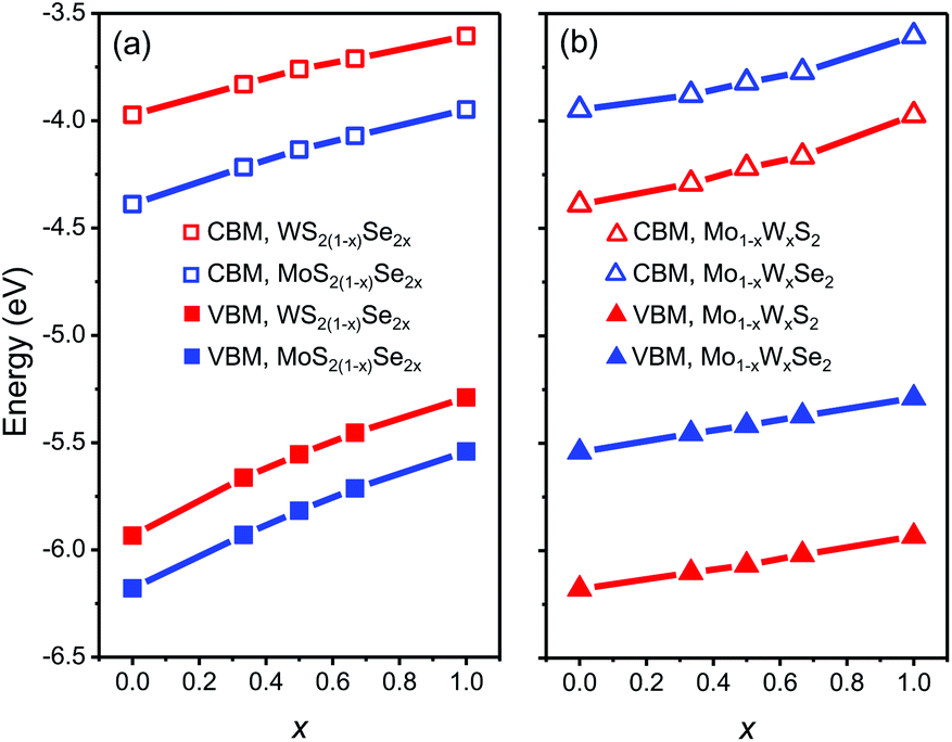 | ||
| Fig. 4 The CBM and VBM as a function of composition x for the mixed (a) anion and (b) cation alloys, respectively (zero energy is the vacuum level). | ||
We determine the heterojunction band alignment from the band edge data for all six heterojunctions of two different TMD pseudo-binary alloy monolayers. While it is possible to fabricate heterojunctions where each side is from the same TMD pseudo-binary alloy system with different compositions (e.g. Mo0.3W0.7S2/Mo0.5W0.5S2), we do not consider such junctions since they are inevitably type II (both the VBM and CBM have the same monotonicity with respect to composition – see Fig. 4). The band alignment type and the effective bandgap (difference between the lowest CBM and highest VBM of the two monolayers) as a function of composition are shown in Fig. 5 for all six TMD pseudo-binary alloy heterojunctions. Among these, only three pseudo-binary alloy pairs exhibit both type I and type II heterojunctions; these are MoS2(1−y)Se2y/WS2(1−x)Se2x, WS2(1−y)Se2y/Mo(1−x)WxSe2 and MoS2(1−y)Se2y/Mo(1−x)WxS2; the others yield only type II heterojunctions.
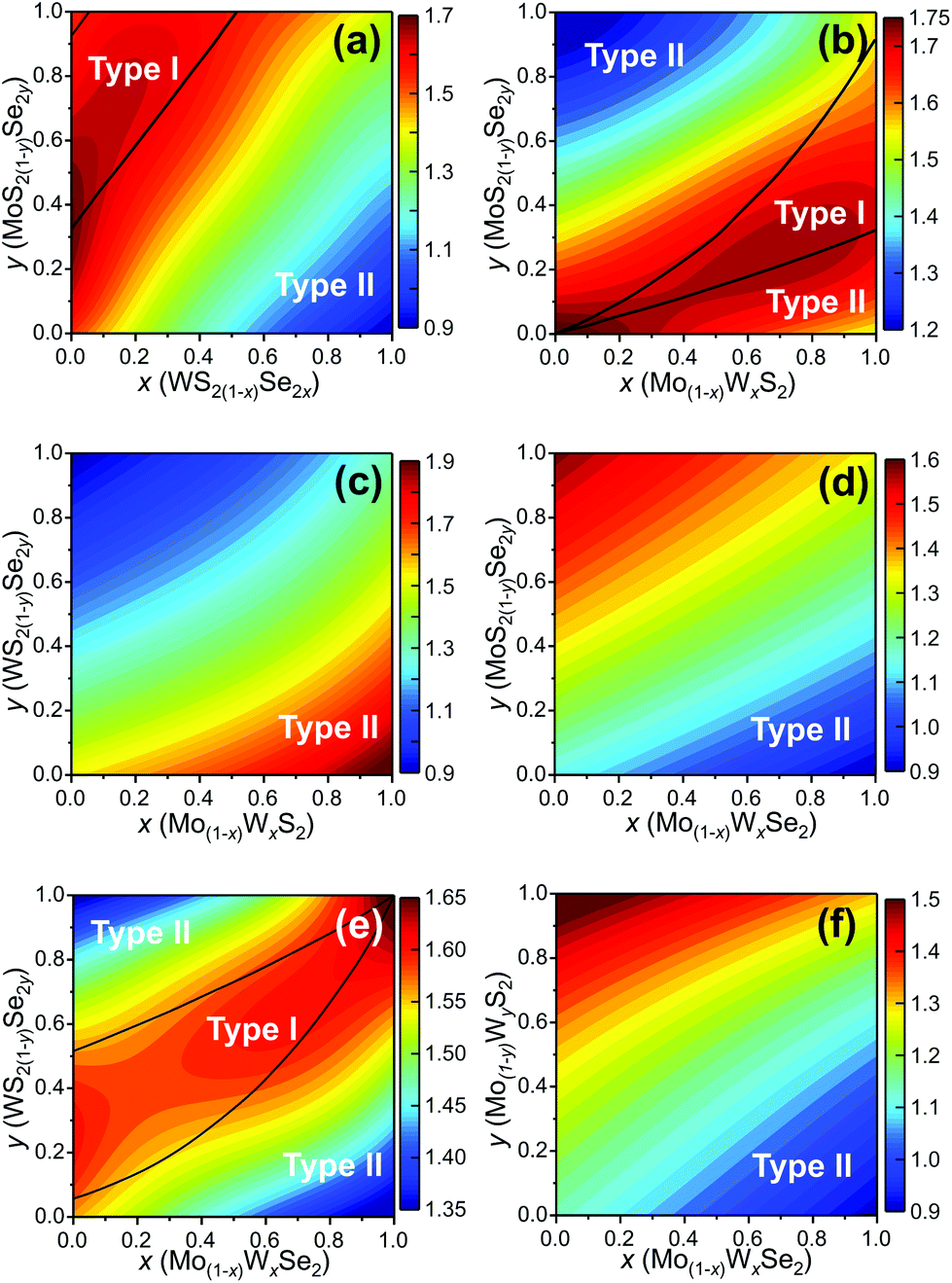 | ||
| Fig. 5 (a)–(f) The pseudo-binary heterojunction type diagrams for all six possible pseudo-binary alloy heterojunctions. The contours show the effective bandgap as a function of composition (fit to 25 compositions each). The black curves indicate the type I/II transition boundaries, corresponding to the zero contour lines of the CBM difference or VBM difference. | ||
The type I/type II transition in MoS2(1−y)Se2y/WS2(1−x)Se2x heterostructures can be easily understood. The MoSe2/WS2(1−x)Se2x (along the y = 1 axis) heterojunction corresponds to the case shown in Fig. 1(a), as does the MoS2(1−y)Se2y/WS2 (along the x = 0 axis) heterojunction. The type I region is near the top left corner of Fig. 5(a) because the CBM difference between MoSe2 and WS2 is relatively small. This implies that relatively small anion doping into WS2 or MoSe2 can convert the MoSe2/WS2 heterojunction to type I.
Like in the MoS2(1−y)Se2y/WS2(1−x)Se2x pseudo-binary heterojunction case, we also find a transition in heterojunction type for MoS2(1−y)Se2y/Mo(1−x)WxS2. Such a transition is not surprising in light of the fact that the CBM (VBM) for MoS2 is below that for WS2 and MoSe2 is above that for WS2; this implies that at some composition {x1, y1} ({x2, y2}) the CBM (VBM) difference between these two alloys must be zero. Examination of Fig. 5(b) shows that there are compositions y for which heterojunction are type I over the entire composition range x. Similarly, there are compositions x for which heterojunction are type I over nearly the entire composition range y. Note that the type I composition range shrinks to zero at the bottom left corner of Fig. 5(b), as it must since (x = 0, y = 0) the vertical heterojunction is simply a homogeneous MoS2 bilayer (i.e., a homo- rather than hetero-junction). A similar argument pertains to the WS2(1−y)Se2y/Mo(1−x)WxSe2 pseudo-binary vertical heterojunction case (Fig. 5(e)) except that in this case it is the (x = 1, y = 1) limit that the heterojunction is actually a WSe2 bilayer.
In addition to modifying the heterojunction from type II to type I by manipulating the compositions in the {MoW}{SeS}2 TMD pseudo-binary alloy system, changing composition also presents opportunities to tune the CBM (VBM) difference and effective bandgap of the heterojunction (which, for example, gives control of the light emission wavelength in type I heterojunctions). The effective bandgap of TMD pseudo-binary alloy heterojunctions are shown as the contours in Fig. 5 as a function of alloy composition {x, y}. The type I heterojunctions exhibit effective bandgaps in the 1.6–1.8 eV range; while the effective range of type II heterojunction bandgaps can be tuned over a much great range 0.9–2.0 eV. The variations of the CBM and VBM across the entire range of TMD monolayer compositions are reported in the ESI.†
2.4 Quaternary alloys
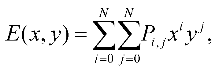
Now we further extend our result to quaternary alloys (Mo(1−x)WxS2(1−y)Se2y) and their heterojunctions. Such a quaternary TMD was recently synthesized via chemical vapor deposition.30 Compared to the pseudo-binary alloys, varying both x and y in a quaternary alloy provides greater flexibility for tuning the bandgap and band offsets to obtain type I TMD heterojunctions (such quaternary systems may also lead to lower synthesis temperatures30).We first calculated the CBM and VBM of the quaternary Mo(1−x)WxS2(1−y)Se2y TMD alloy monolayers as a function of x and y (see Fig. 6), where the alloy structures were represented using the SQS approach. In addition to the data points obtained for the pseudo-binary alloys (present along the axes in Fig. 6), we add five quaternary alloy data points at a small set of additional (x, y) pairs (21 data points in total). Because the CBM and VBM are smooth, monotonic functions of x and y, they are well fit by a low order N polynomial
 | (1) |
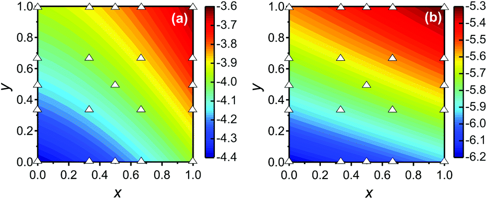 | ||
| Fig. 6 Contour plots of the (a) CBM and (b) VBM of quaternary alloy Mo(1−x)WxS2(1−y)Se2y monolayers based on the ab initio data at the compositions indicated by the open triangles. | ||
| N | P 00 | P 01 | P 10 | P 11 | P 02 | P 20 | P 12 | P 21 | P 22 | RMSE | |
|---|---|---|---|---|---|---|---|---|---|---|---|
| CBM | 1 | −4.3940 | 0.4342 | 0.4084 | −0.0679 | 0.0321 | |||||
| VBM | −6.1630 | 0.6434 | 0.2561 | 0.0018 | 0.0269 | ||||||
| CBM | 2 | −4.3860 | 0.5536 | 0.2262 | −0.0938 | −0.1162 | 0.1842 | 0.0027 | 0.0113 | 0.0118 | 0.0118 |
| VBM | −6.1800 | 0.8124 | 0.2191 | 0.1151 | −0.1726 | 0.0288 | −0.0862 | −0.0532 | 0.0261 | 0.0029 |
Compared to that of the pseudo-binary alloys, the quaternary system exhibits larger ranges of both the CBM (−3.6 to −4.4 eV) and VBM (−5.3 to −6.2 eV). Unfortunately, such band alignment diagrams are 4-dimensional and not easily visualized. However, the alignment and gap value can be easily determined by using above band edge data. The heterojunction is of type I if (ΔECBM)(ΔEVBM) < 0 (or type II otherwise), where ΔECBM and ΔEVBM are the CBM and VBM difference, respectively (see eqn (1)).
2.5 Direct vs. indirect bandgaps: twisted bilayers
To this point, we focused largely on the determination of band edge alignment at the K point. However, it is unclear in what (if any) composition ranges the proposed type I heterojunctions have direct bandgaps. In these type I TMD alloy heterojunctions, the bandgap is direct when the VBM at K is higher than the VBM at Γ (recall that the VBM at K is independent of interlayer interaction and is only a function of composition x). The VBM at Γ is determined by interlayer interactions, which may be affected by rotation of one monolayer with respect to the other (about the monolayer normal). Monolayer rotation disrupts the alignment of orbitals directed normal to the interface (this is relevant to the VBM at Γ); rotation effectively decouples monolayers and weakens interlayer interactions, as reported for bilayer graphene. In MoS2/WS2, the two monolayers have no lattice mismatch; the heterojunction has coherent AA′ stacking (where the transition metal in one monolayer lies directly above the chalcogenide atoms in the other monolayer). In this case, the interlayer interactions are strong and heterojunction has indirect bandgap. However, when the layers are rotated with respect to one another, the coherent AA′ stacking is replaced by an incoherent (or irrational) stacking except at a countable set of rotation angles. This irrational stacking decouples the two monolayers and weakens the interlayer interaction at Γ. Rotations between monolayers in vertical heterojunction are very common as a result of heterojunction production methods (fabrication by mechanical exfoliation and bonding commonly results in monolayer rotations). Layer rotation may even be present based on energetic considerations (e.g., rotated epitaxy to accommodate misfit when two monolayers have different lattice constants). So generally, the VBM at Γ is a function of both composition and rotation.We investigate the dependence of the VBM at Γ on rotation using a supercell of sufficient size to accommodate the twisted bilayer. We focus first on heterojunctions of pure TMD heterojunctions in order to validate our approach and then apply it to TMD alloy heterojunctions. In particular, we first investigate the lattice-matched case for a MoS2/WS2 heterojunction example. The two layers are rotated with respect to one another by a rotation angle, θ, the angle between armchair directions in the two monolayers (θ = 0 corresponds to the coherent AA′ stacking). Since the two layers are rotated relative to one another, we account for supercell band folding in the evaluation of the VBM at Γ and K using an effective band structure approach.53 The states are first projected from the heterojunction onto each monolayer and unfolded relative to the primitive cell of each monolayer.
The VBM for the MoS2/WS2 heterojunction at the Γ and K points is shown in Fig. 7(a) for several rotation angles. These angles are chosen such that the rotated heterojunction supercell has small lattice misfit (≤0.5%) between two monolayers and the supercell sufficiently small for (reasonable) DFT calculations. The VBM at K is nearly rotation angle independent at a value close to that of a WS2 monolayer at K; this further validates the Anderson's rule approach at K. While the VBM at Γ is higher than that at K at θ = 0, the VBM at Γ changes significantly with respect to θ near θ = 0 and 60°, but nearly constant at intermediate rotation angles. In this intermediate angle range, the VBM at Γ is still higher than that at K, but the difference is significantly smaller than that at θ = 0 (0.03 vs. 0.16 eV). However, increasing θ beyond some critical angle, the VBM at Γ drops below that at K. The lowest VBM at Γ (−5.56 eV) is 0.22 eV higher than that in WS2 (−5.78 eV). This is because that, despite being weakened by rotation, interaction between layers still exists for the VBM at Γ. We note that lattice-matched monoloyers are rare in the entire composition space (along a small set of curves in the two-dimensional bilayer pseudo-binary composition space). For example, lattice-matching in MoS2(1−y)Se2y/WS2(1−x)Se2x occurs along y ≈ x (Fig. 5(a)).
 | ||
| Fig. 7 The VBM at Γ (black) and K (red) for (a) lattice-matched MoS2/WS2 heterojunctions and (b) lattice-mismatched MoS2/WSe2 heterojunctions as a function of rotation angle θ, all the energy levels are aligned with respect to the vacuum level. An index (blue) is defined to measure the interlayer interaction strength as well as VBM at Γ. (c) Schematic representation of geometric model: the red and blue circles of radius R+ and R− represent circles placed on calcogenide atoms in top and bottom monolayer, respectively. The rotation angle θ is defined as zero when there is minimum overlaping area in lattice-matched case, where the structure is coherent AA′ stacking. (d) The composition regions of global VBM at K (cyan) and Γ (pink) in MoS2(1−y)Se2y/WS2(1−x)Se2x alloy heterojunction of about 30° rotation. The composition region obtained by fitting the band edge data from four pure TMD heterojunctions (corners) (30° rotation for lattice-mismatched cases and 28° rotation for lattice-matched cases). | ||
As an example of a more common lattice-mismatched case, we examine MoS2/WSe2 heterojunctions (see Fig. 7(b)). Note that because the two monolayers have different lattice constants, θ = 0 does not correspond to a coherent structure as in the lattice-matched case (there is no θ = 0 data point in the figure since there requires a very large DFT supercell). As in the lattice-matched case, the VBM at K is nearly independent of rotation angle (−4.88 eV). For the three rotation angles examined here, the VBM at Γ is nearly independent of rotation angle and is consistently ∼0.3 eV lower than that at K; i.e., the VBM is at K for all θ. This independence of the VBM at Γ on θ may be attributed to the fact that the lattice-mismatch between the layers insures that the two layers will be incoherent (all incoherent cases have similar interlayer interaction strength). Any coherency will occur at a countable set of rotation angles and in very large periodic cells.
As our data in Fig. 7 are sparse, we further examine the effect of rotation on the basis of a simple geometric model to account for interlayer interactions on the VBM at Γ. Since the interlayer interactions are dominated by chalcogenide atom orbitals directed normal to the monolayer. We place circles of radius R+ and R− at the location of each chalcogen in the top and bottom monolayer, respectively, to crudely represent the lateral extent of the orbitals (Fig. 7c). We then examine the overlap (area) between the circles as a measure of the interlayer interaction strength. We define the interlayer interaction function as 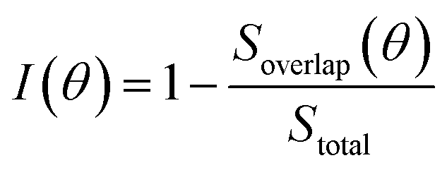 , where Soverlap(θ) is the overlap area between circles in two monolayers, and Stotal is the total area of circles in top monolayer at fixed material parameters (lattice constant ratio a−/a+, circle radius ratio R−/R+ and lattice constant to radius ratio R+/a+). In our examples, we set
 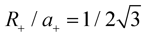 and R−/R+ = 1 and a−/a+ = 1 or 1.044 for lattice-matched and -mismatched cases, respectively. In the lattice-matched case (Fig. 7a), I(θ = 0) = 1 and drops abruptly to I = 0.7, remains nearly θ-independent until θ ≈ 60° where it drops to θ(60°) = 0. For the lattice-mismatched case, I(θ) is independent of θ over the entire angle range (apart from small variations near 0 and 60°). These trends are consistent with our DFT data calculations for the VBM at Γ (Fig. 7a and b). This confirms the conclusion that the VBM at Γ is nearly independent of rotation angle and misfit for all TMD bilayers, except for a small set of special cases (e.g., lattice-matched case at θ = 0). Note, since this index reflects bilayer registry, it also is an indicator of the relative energy of the different configurations (configurations of larger index have lower energy). These results imply that lattice-mismatched heterojunctions with different rotations have similar energy and are nearly equally stable.
We now consider the question of which alloy bilayer heterojunctions have direct bandgaps based on the assumption that the two monolayers are rotated with respect to one another by an angle not too near θ = 0 or 60°. As an example, we focus on the MoS2(1−y)Se2y/WS2(1−x)Se2x alloy heterojunction with about 30° rotation. We first calculate the band edge of pure TMD heterojunctions of about 30° rotation (30° for lattice-mismatched cases and 28° for lattice-matched cases). Then use these data to estimate the composition region (via a simple spline) where the global VBM located at Γ or K (Fig. 7d). Only the MoS2/WS2 heterojunction has a higher VBM at Γ than the VBM at K such that the composition region where the VBM at Γ is limited to near the bottom left corner of Fig. 7d. We also ensure that the CBM is located at K for all cases here (WS2/MoSe2 has degenerate global CBM states). As the type I composition region is located near the top left corner of the diagram (Fig. 5a) for this alloy bilayer heterojunction, the overlap between these regions (type I and global VBM at Γ) should be very limited. Hence, the type I heterojunctions in this alloy system should exhibit direct bandgaps. In particular, in the MoS2(1−y)Se2y/WS2(1−x)Se2x alloy heterojunction case, type I direct bandgaps should be achievable in the following composition range 1.34x + 0.33 < y < 1.17x + 0.93, independent of rotation angle (as long as the lattice parameter misfit is not 0).
Note that this direct bandgap only applies to type I heterojunctions, where the global CBM and VBM are located in the same monolayer. In type II heterojunctions (where the VBM and CBM at K belong to different monolayers), rotation implies that the K points in the two monolayers are not identical. Such rotated type II heterojunctions will have an indirect bandgap even when the global VBM is located at K. Fortunately, most applications of type II heterojunctions are not optical and, hence, direct bandgaps are unnecessary.
3 Conclusion
While bilayer, vertical heterojunctions of {Mo, W}{S, Se}2 monolayers have been widely discussed for microelectronics and optoelectronic applications, all such binary monolayer heterojunctions are limited to type II band alignment. We examined VBM and CBM band alignment in heterojunctions where each monolayer is from the Mo(1−x)WxS2(1−y)Se2y quaternary alloy family. The VBM and CBM at the K point and the bandgap were shown to vary continuously with composition over the entire alloy space. The effective bandgap in these TMD alloy heterojunctions is tunable from 0.9 to 2.0 eV. We demonstrate that in half of the pseudo-binary cases, there are broad composition ranges for which type I vertical TMD heterojunction band alignment occurs and provide a general framework to predict the heterojunction band alignment.Direct bandgap type I heterojunction are preferred for light-emitting applications. Indirect bandgaps may arise because of interactions between monolayers (not captured by Anderson's rule); orbital overlap between chalcogens on the two layers give rise to a VBM at the Γ (rather than K) point. On the other hand, the VBM at the K point is largely unaffected by joining the monolayers into a heterojunction. The degree of orbital overlap is strongly influenced by the relative rotation of one monolayer with respect to the other. Here we determined the band edges as a function of rotation angle for both lattice-matched and -mismatched bilayers, and provided a simple, predictive geometrical model to capture this effect. In the lattice-matched case, the VBM at Γ is independent of rotation angle except very near the special angles of 0 and 60°. In the lattice-mismatched case, the resultant incommensurability ensures that VBM at Γ is a constant. This is consistent with the weak van der Waals interactions between layers and the high in-plane monolayer stiffness that resists strained heteroepitaxy. Based on these conclusions and data, we predict that type I alloy heterojunction of direct bandgap are achievable over a wide range of TMD composition and/or rotation space.
The present results provide alloying and/or monolayer rotation approach to creating direct bandgap, type I TMD alloy-based heterojunctions. In particular, we provide alloy composition ranges in the pseudo-binary and quaternary {Mo, W}{S, Se}2 system for which such direct, type I heterojunctions should be achievable.
4 Methods
Density functional theory (DFT) calculations were performed using the Vienna Ab Initio Simulation Package (VASP)54,55 using both a plane-wave basis set and the projector augmented wave method.56,57 The Strongly Constrained and Appropriately Normed (SCAN) semilocal density functional was employed51 with a 41 × 41 × 1 Γ-centered k-point mesh (in the primitive cell) and an energy cutoff of 520 eV for band edge calculations. A vacuum layer of at least 20 Å perpendicular to the monolayer was employed. Atomic structures were relaxed until the total force on each atom was ≤0.01 eV Å−1.The heterojunction data in Fig. 2 and 7, were obtained using the PBE functional with an energy cutoff of 500 eV. The Tkatchenko–Scheffler method was employed to describe the van der Waals interaction between monolayers. For the supercells with rotation, because the two monolayer are twisted relative to each other in the rotated bilayer heterojunction, the calculated band structure is folded. To unfold the bands and extract the desired VBM states, we employed the BandUP code.58,59 Here, the heterojunction supercell states are projected to the Brillouin zone of each of the monolayers and unfolded to retrieve the effective band structure53 in their respective primitive cells. When projected to different monolayers, the k-points of the two monolayers (e.g., the high symmetry point K) are not identical except at the Γ point.
Both Special Quasirandom Structures43,44 (SQS) and cluster expansion42 approaches were employed, within the Alloy Theoretic Automated Toolkit (ATAT).60 For the SQS, we ensured that the correlation function for the first-third nearest neighbor pair clusters is consistent with a perfectly random alloy, and minimized the correlation function difference (compared with the perfectly random alloy) of the two most compact triplet clusters (i.e., the first and second nearest triplet). For the pseudo-binary alloys at compositions x = 1/3, 2/3 and 1/2, we used a 3 ×  × 1, 3 ×
  × 1 and 4 ×
  × 1 rectangular supercell, respectively. For the quaternary alloys, at composition (1/3, 1/3), (2/3, 1/3), (1/3, 2/3) and (2/3, 2/3), a 3 ×
  × 1 rectangular supercell was used and for the composition (1/2, 1/2), a 4 ×
  × 1 rectangular supercell was employed. For the cluster expansion and formation enthalpy calculations for the alloys, we employed the Perdew–Burke–Ernzerhof functional (PBE)47 with an energy cutoff of 350 eV.
Conflicts of interest
There are no conflicts to declare.Acknowledgements
This work was supported in its entirety as part of the Center for the Computational Design of Functional Layered Materials, an Energy Frontier Research Center funded by the U.S. Department of Energy (DOE), Office of Science, Basic Energy Sciences (BES) under Award DE-SC0012575.References
- J. D. Werking, C. R. Bolognesi, L.-D. Chang, C. Nguyen, E. L. Hu and H. Kroemer, IEEE Electron Device Lett., 1992, 13, 164–166 CAS.
- A. Nourbakhsh, A. Zubair, M. S. Dresselhaus and T. Palacios, Nano Lett., 2016, 16, 1359–1366 CrossRef CAS PubMed.
- D. Jariwala, A. R. Davoyan, J. Wong and H. A. Atwater, ACS Photonics, 2017, 4, 2962–2970 CrossRef CAS.
- F. Withers, O. Del Pozo-Zamudio, A. Mishchenko, A. P. Rooney, A. Gholinia, K. Watanabe, T. Taniguchi, S. J. Haigh, A. K. Geim, A. I. Tartakovskii and K. S. Novoselov, Nat. Mater., 2015, 14, 301–306 CrossRef CAS PubMed.
- P. Waltereit, O. Brandt, A. Trampert, H. T. Grahn, J. Menniger, M. Ramsteiner, M. Reiche and K. H. Ploog, Nature, 2000, 406, 865–868 CrossRef CAS PubMed.
- Y. J. Song, M. R. Park, E. Guliants and W. A. Anderson, Sol. Energy Mater. Sol. Cells, 2000, 64, 225–240 CrossRef CAS.
- R. Cheng, D. Li, H. Zhou, C. Wang, A. Yin, S. Jiang, Y. Liu, Y. Chen, Y. Huang and X. Duan, Nano Lett., 2014, 14, 5590–5597 CrossRef CAS PubMed.
- A. K. Geim and I. V. Grigorieva, Nature, 2013, 499, 419–425 CrossRef CAS PubMed.
- Y. Gong, J. Lin, X. Wang, G. Shi, S. Lei, Z. Lin, X. Zou, G. Ye, R. Vajtai, B. I. Yakobson, H. Terrones, M. Terrones, B. K. Tay, J. Lou, S. T. Pantelides, Z. Liu, W. Zhou and P. M. Ajayan, Nat. Mater., 2014, 13, 1135–1142 CrossRef CAS PubMed.
- P. Rivera, K. L. Seyler, H. Yu, J. R. Schaibley, J. Yan, D. G. Mandrus, W. Yao and X. Xu, Science, 2016, 351, 688–691 CrossRef CAS PubMed.
- K. F. Mak, C. Lee, J. Hone, J. Shan and T. F. Heinz, Phys. Rev. Lett., 2010, 105, 136805 CrossRef PubMed.
- A. Splendiani, L. Sun, Y. Zhang, T. Li, J. Kim, C.-Y. Chim, G. Galli and F. Wang, Nano Lett., 2010, 10, 1271–1275 CrossRef CAS PubMed.
- C. Huang, S. Wu, A. M. Sanchez, J. J. P. Peters, R. Beanland, J. S. Ross, P. Rivera, W. Yao, D. H. Cobden and X. Xu, Nat. Mater., 2014, 13, 1096–1101 CrossRef CAS PubMed.
- M.-Y. Li, Y. Shi, C.-C. Cheng, L.-S. Lu, Y.-C. Lin, H.-L. Tang, M.-L. Tsai, C.-W. Chu, K.-H. Wei, J.-H. He, W.-H. Chang, K. Suenaga and L.-J. Li, Science, 2015, 349, 524–528 CrossRef CAS PubMed.
- F. M. Pesci, M. S. Sokolikova, C. Grotta, P. C. Sherrell, F. Reale, K. Sharda, N. Ni, P. Palczynski and C. Mattevi, ACS Catal., 2017, 7, 4990–4998 CrossRef CAS.
- C.-H. Lee, G.-H. Lee, A. M. Van Der Zande, W. Chen, Y. Li, M. Han, X. Cui, G. Arefe, C. Nuckolls, T. F. Heinz, J. Guo, J. Hone and P. Kim, Nat. Nanotechnol., 2014, 9, 676–681 CrossRef CAS PubMed.
- V. O. Özçelik, J. G. Azadani, C. Yang, S. J. Koester and T. Low, Phys. Rev. B, 2016, 94, 035125 CrossRef.
- C. Gong, H. Zhang, W. Wang, L. Colombo, R. M. Wallace and K. Cho, Appl. Phys. Lett., 2013, 103, 053513 CrossRef.
- M.-H. Chiu, C. Zhang, H.-W. Shiu, C.-P. Chuu, C.-H. Chen, C.-Y. S. Chang, C.-H. Chen, M.-Y. Chou, C.-K. Shih and L.-J. Li, Nat. Commun., 2015, 6, 7666 CrossRef CAS PubMed.
- H. M. Hill, A. F. Rigosi, K. T. Rim, G. W. Flynn and T. F. Heinz, Nano Lett., 2016, 16, 4831–4837 CrossRef CAS PubMed.
- P. Rivera, J. R. Schaibley, A. M. Jones, J. S. Ross, S. Wu, G. Aivazian, P. Klement, K. Seyler, G. Clark, N. J. Ghimire, J. Yan, D. G. Mandrus, W. Yao and X. Xu, Nat. Commun., 2015, 6, 6242 CrossRef CAS PubMed.
- D. Kozawa, A. Carvalho, I. Verzhbitskiy, F. Giustiniano, Y. Miyauchi, S. Mouri, A. H. Castro Neto, K. Matsuda and G. Eda, Nano Lett., 2016, 16, 4087–4093 CrossRef CAS PubMed.
- K. Keyshar, M. Berg, X. Zhang, R. Vajtai, G. Gupta, C. K. Chan, T. E. Beechem, P. M. Ajayan, A. D. Mohite and T. Ohta, ACS Nano, 2017, 11, 8223–8230 CrossRef CAS PubMed.
- A. Kutana, E. S. Penev and B. I. Yakobson, Nanoscale, 2014, 6, 5820–5825 RSC.
- X. Duan, C. Wang, Z. Fan, G. Hao, L. Kou, U. Halim, H. Li, X. Wu, Y. Wang, J. Jiang, A. Pan, Y. Huang, R. Yu and X. Duan, Nano Lett., 2015, 16, 264–269 CrossRef PubMed.
- J.-G. Song, G. H. Ryu, S. J. Lee, S. Sim, C. W. Lee, T. Choi, H. Jung, Y. Kim, Z. Lee, J.-M. Myoung, C. Dussarrat, C. Lansalot-Matras, J. Park, H. Choi and H. Kim, Nat. Commun., 2015, 6, 7817 CrossRef PubMed.
- H. Li, X. Duan, X. Wu, X. Zhuang, H. Zhou, Q. Zhang, X. Zhu, W. Hu, P. Ren, P. Guo, L. Ma, X. Fan, X. Wang, J. Xu, A. Pan and X. Duan, J. Am. Chem. Soc., 2014, 136, 3756–3759 CrossRef CAS PubMed.
- Q. Fu, L. Yang, W. Wang, A. Han, J. Huang, P. Du, Z. Fan, J. Zhang and B. Xiang, Adv. Mater., 2015, 27, 4732–4738 CrossRef CAS PubMed.
- Y. Gong, Z. Liu, A. R. Lupini, G. Shi, J. Lin, S. Najmaei, Z. Lin, A. L. Elías, A. Berkdemir, G. You, H. Terrones, M. Terrones, R. Vajtai, S. T. Pantelides, S. J. Pennycook, J. Lou, W. Zhou and P. M. Ajayan, Nano Lett., 2013, 14, 442–449 CrossRef PubMed.
- S. Susarla, A. Kutana, J. A. Hachtel, V. Kochat, A. Apte, R. Vajtai, J. C. Idrobo, B. I. Yakobson, C. S. Tiwary and P. M. Ajayan, Adv. Mater., 2017, 29, 1702457–1702457 CrossRef PubMed.
- H.-P. Komsa and A. V. Krasheninnikov, J. Phys. Chem. Lett., 2012, 3, 3652–3656 CrossRef CAS PubMed.
- J. Kang, S. Tongay, J. Li and J. Wu, J. Appl. Phys., 2013, 113, 143703 CrossRef.
- B. Zheng, C. Ma, D. Li, J. Lan, Z. Zhang, X. Sun, W. Zheng, T. Yang, C. Zhu and G. Ouyang, et al. , J. Am. Chem. Soc., 2018, 140, 11193–11197 CrossRef CAS PubMed.
- R. Decker, Y. Wang, V. W. Brar, W. Regan, H.-Z. Tsai, Q. Wu, W. Gannett, A. Zettl and M. F. Crommie, Nano Lett., 2011, 11, 2291–2295 CrossRef CAS PubMed.
- J. Xue, J. Sanchez-Yamagishi, D. Bulmash, P. Jacquod, A. Deshpande, K. Watanabe, T. Taniguchi, P. Jarillo-Herrero and B. J. LeRoy, Nat. Mater., 2011, 10, 282 CrossRef CAS PubMed.
- S. Dai, Y. Xiang and D. J. Srolovitz, Nano Lett., 2016, 16, 5923–5927 CrossRef CAS PubMed.
- S. Dai, Y. Xiang and D. J. Srolovitz, Phys. Rev. B, 2016, 93, 085410 CrossRef.
- R. L. Anderson, IBM J. Res. Dev., 1960, 4, 283–287 CAS.
- M.-H. Chiu, W.-H. Tseng, H.-L. Tang, Y.-H. Chang, C.-H. Chen, W.-T. Hsu, W.-H. Chang, C.-I. Wu and L.-J. Li, Adv. Funct. Mater., 2017, 27, 1603756–1603756 CrossRef.
- J.-H. Yang and B. I. Yakobson, Chem. Mater., 2018, 30, 1547–1555 CrossRef CAS.
- W. Tan, Z. Wei, X. Liu, J. Liu, X. Fang, D. Fang, X. Wang, D. Wang, J. Tang and X. Fan, Sci. Rep., 2017, 7, 15124 CrossRef PubMed.
- J. M. Sanchez, F. Ducastelle and D. Gratias, Phys. A, 1984, 128, 334–350 CrossRef.
- A. Zunger, S.-H. Wei, L. G. Ferreira and J. E. Bernard, Phys. Rev. Lett., 1990, 65, 353 CrossRef CAS PubMed.
- S.-H. Wei, L. G. Ferreira, J. E. Bernard and A. Zunger, Phys. Rev. B: Condens. Matter Mater. Phys., 1990, 42, 9622 CrossRef CAS PubMed.
- S.-H. Su, Y.-T. Hsu, Y.-H. Chang, M.-H. Chiu, C.-L. Hsu, W.-T. Hsu, W.-H. Chang, J.-H. He and L.-J. Li, Small, 2014, 10, 2589–2594 CrossRef CAS PubMed.
- L.-Y. Gan, Q. Zhang, Y.-J. Zhao, Y. Cheng and U. Schwingenschlögl, Sci. Rep., 2014, 4, 6691 CrossRef CAS PubMed.
- J. P. Perdew, K. Burke and M. Ernzerhof, Phys. Rev. Lett., 1996, 77, 3865 CrossRef CAS PubMed.
- J. P. Perdew and M. Levy, Phys. Rev. Lett., 1983, 51, 1884 CrossRef CAS.
- P. Mori-Sánchez, A. J. Cohen and W. Yang, Phys. Rev. Lett., 2008, 100, 146401 CrossRef PubMed.
- F. Ceballos, M. Z. Bellus, H.-Y. Chiu and H. Zhao, Nanoscale, 2015, 7, 17523–17528 RSC.
- J. Sun, A. Ruzsinszky and J. P. Perdew, Phys. Rev. Lett., 2015, 115, 036402 CrossRef PubMed.
- J. Sun, R. C. Remsing, Y. Zhang, Z. Sun, A. Ruzsinszky, H. Peng, Z. Yang, A. Paul, U. Waghmare, X. Wu, M. L. Klein and J. P. Perdew, Nat. Chem., 2016, 8, 831–836 CrossRef CAS PubMed.
- V. Popescu and A. Zunger, Phys. Rev. Lett., 2010, 104, 236403 CrossRef PubMed.
- G. Kresse and J. Furthmüller, Comput. Mater. Sci., 1996, 6, 15–50 CrossRef CAS.
- G. Kresse and J. Furthmüller, Phys. Rev. B: Condens. Matter Mater. Phys., 1996, 54, 11169 CrossRef CAS PubMed.
- P. E. Blöchl, Phys. Rev. B: Condens. Matter Mater. Phys., 1994, 50, 17953 CrossRef PubMed.
- G. Kresse and D. Joubert, Phys. Rev. B: Condens. Matter Mater. Phys., 1999, 59, 1758 CrossRef CAS.
- P. V. Medeiros, S. Stafström and J. Björk, Phys. Rev. B: Condens. Matter Mater. Phys., 2014, 89, 041407 CrossRef.
- P. V. Medeiros, S. S. Tsirkin, S. Stafström and J. Björk, Phys. Rev. B: Condens. Matter Mater. Phys., 2015, 91, 041116 CrossRef.
- A. Van De Walle, M. Asta and G. Ceder, CALPHAD: Comput. Coupling Phase Diagrams Thermochem., 2002, 26, 539–553 CrossRef CAS.
Footnote |
| † Electronic supplementary information (ESI) available. See DOI: 10.1039/C9NR08345F |
| This journal is © The Royal Society of Chemistry 2020 |