
Plasma driven nano-morphological changes and photovoltaic performance in dye sensitized 2D-layered dual oxy-sulfide phase WS2 films
Gopika
Gopakumar
,
Shantikumar V.
Nair
and
Mariyappan
Shanmugam
 *
*
Amrita Centre for Nanosciences and Molecular Medicine, Amrita Vishwa Vidyapeetham, Kerala-682041, India. E-mail: mshanmugham@aims.amrita.edu
First published on 14th November 2019
Abstract
The present work examined dye sensitized 2D layered tungsten disulfide (WS2) as a photo-anode in solar cells with no use of nanocrystalline metal oxides as electron acceptors such as titanium dioxide. It is observed that coating WS2 directly onto a fluorine doped tin oxide (FTO) transparent conductor, annealed at 530 °C, resulted in a mixed oxy-sulfide dual phase as confirmed by transmission electron microscopy and X-ray diffraction studies. Further studies on the surface morphology of the dual phase WS2–WO3 film showed a random distribution of platelets which further shaped into precisely regulated hexagonal platelets upon plasma treatment. High resolution transmission electron microscopic studies elucidated two different phases, WS2 and WO3, with d-spacing values of 0.26 nm and 0.37 nm, respectively. A well-defined grain boundary was also observed which separated the oxy-sulfide phase in the sample. The dual WS2–WO3 phase films showed optical absorption in the wavelength range of 350 nm–800 nm with a systematic increase in plasma exposure duration. Photovoltaic devices fabricated using the WS2–WO3 mixed phase photo-anodes resulted in 0.61% efficiency (η) which further was observed to be sensitive to the plasma exposure as it was observed that the 20 minute plasma treated sample increased the η value to 0.67%. Plasma treatment on the dual-phase samples orients and modifies the shapes of the platelets with a significant change in the surface which eventually influences the charge transport in resulting photovoltaic devices and thus the variation with respect to exposure duration.
1 Introduction
Cost effective third generation photovoltaic technologies, particularly dye and quantum dot sensitized, have shown their potential competiveness to well-established wafer and thin film based energy conversion devices.1–3 Wide bandgap (3 eV–3.8 eV) metal oxide nanocrystalline electron acceptors in dye sensitized solar cells (DSSCs) are very familiar and highly suitable for dye coating due to their large surface area which potentially determines the photo-current in DSSCs.4–6 Although the nanocrystalline metal oxides are used mainly for dye adsorption, they facilitate charge transport in DSSCs via a diffusion dominated mechanism.7,8 It has been demonstrated that photocurrent in DSSCs is highly sensitive to the optical absorption of organic sensitizers and the charge transport is mainly dependent on the electronic quality of nanocrystalline metal oxides as they act as electron acceptors.9–11Morphology, thickness, defects, crystallinity, surface area and phase of the metal oxide electron acceptors play a vital role in charge transport during solar cell operation.12–15 Thus, it is evident that electron acceptors are critical functional materials in DSSCs to achieve effective charge transport and overall photovoltaic performance. However, major disadvantages in such nanocrystalline electron acceptors are surface state mediated charge carrier recombination which is a detrimental effect that suppresses the performance of DSSCs.16–19 Previous studies have shown the effect of surface states as recombination centers in nanocrystalline electron acceptors.20,21 Replacing such metal oxide based electron acceptors in excitonic solar cells is rather challenging and it is an unwanted and technically challenging issue as the desired properties are more dominating than the detrimental effects that are associated with them.
Recent research has identified hexagonal two dimensional (2D) lattice structured functional materials from the group of transition metal dichalcogenides which show exotic structural, optical and electrical properties that are attractive for energy conversion technology.22–25 2D layered semiconductors are well known for effective light absorption even at extremely low thickness due to their direct bandgap values with extremely high optical absorption coefficient.26,27 Tungsten disulfide (WS2), an important 2D layered semiconductor, has shown a variety of applications including light emitting diodes, solar cells, sensors and actuators.28–30 WS2 has shown effective photo-absorption in a spectral window of 350 nm–800 nm with dominant characteristic peaks at 530 nm and 635 nm.31 It has shown a charge carrier mobility of ∼140 cm2 V−1 s−1 at low temperature with a possibility of achieving up to 300 cm2 V−1 s−1 for the case of bilayer stacks.32 Effective light absorption and efficient charge transport are two major parameters that make a material a potential candidate for photovoltaic applications. Various synthesis routes to obtain WS2 have been reported including micro-mechanical/chemical exfoliation, chemical vapor deposition and few wet-chemical methods.33–36 Tungsten oxide (WO3), an n type material having optical absorption in the near UV region and having higher carrier mobility, has been explored in many applications such as sensors,36 photocatalysis,37 and photovoltaics.38 There have been many reports on the formation of WS2 from WO3,39–41 but few explain the formation of WO3 from WS2.42,43 Out of which, there have been very few reports exploring the applications of the dual WS2–WO3 phase.44
It is emphasized that the photovoltaic applications of dye sensitized 2D layered WS2 have not been demonstrated and further it has been realized that understanding the effect of the dual oxy-sulfide phase of the 2D material on solar cell performance is an important scientific merit to achieve. The present work assessed photo-physical characteristics of the N719 dye coated WS2 by various characterization methods and interestingly a mixed dual phase was observed. A systematic study was performed in the mixed dual phase WS2–WO3 as an electron acceptor in solar cells. Changes in the photovoltaic characteristics of the N719 dye coated dual phase 2D layered WS2–WO3 were assessed and further changes due to plasma treatment were examined. The present work also is an essential technical platform in which the compatibility of 2D layered semiconductors and organic photo-active molecules is envisaged through various material and device characteristics. Modifications in the surface of semiconductors using plasma at the nanoscale level and their influence on photovoltaic mechanisms are also demonstrated to develop energy conversion devices based on emerging 2D layered semiconductors.
2 Experimental section
(i) Fabrication of solar cells using dye sensitized WS2 film
WS2 powder was obtained from Alfa Aesar and further crushed to obtain ultra-fine powder. It was then mixed with polyester to make a colloidal paste. The colloidal paste was coated onto fluorine doped tin oxide (FTO) covered glass substrates by a doctor blade method. This sample was annealed at 530 °C for one hour in an air atmosphere. The FTO/WS2 sample was immersed in an N719 dye bath to sensitize. Iodide/tri-iodide electrolyte was used as a hole transporting material with 50 nm thick Pt coated glass substrate as a counter electrode. N719 dye coated WS2 and the Pt coated counter electrode were coupled together with iodide/tri-iodide electrolyte filled in-between to perform the solar cell for measurements.(ii) Fabrication of solar cells using plasma processed WS2 film
To examine the effect of plasma treatment on a WS2 film, it was exposed to plasma generated using argon gas with a flow rate of 30 sccm and 10 W RF-power. The exposure duration was varied to 20, 40 and 60 minutes. The three different WS2 films were used to fabricate solar cells after sensitizing with N719 dye. The other fabrication steps are the same as those explained in section (i).(iii) Materials and solar cell characterization studies
Diffraction patterns of the samples involved in the present work were recorded using a PANalytical X'Pert PRO X-Ray Diffractometer (XRD). Surface morphology of the WS2 films was characterized using a Jeol-JSM-6490-LA scanning electron microscope (SEM). High resolution transmission electron microscopic (TEM) studies were performed on the WS2 films using a Tecnai G2 TF20 S-Twin transmission electron microscope. Optical characteristics of the WS2 films were studied using a PerkinElmer Lambda-750 UV-Visible spectrometer. The current density–voltage (J–V) measurements of the solar cells were performed under 1-Sun simulated light (AM 1.5 G) using a solar simulator (Newport Oriel Class A) and a digital source meter (Keithley 2400).3 Results and discussion
Fig. 1(a) shows the stacked XRD patterns obtained from pristine WS2 film which turned out to be mixed WS2–WO3 upon 530 °C annealing for one hour. As referenced in JCPDS 08-0237, the dominant peaks observed at 14.3°, 29°, and 33.7° correspond to (002), (004) and (101), respectively. It is evident from the XRD pattern shown in Fig. 1(a) second row that the pristine WS2 phase was modified by the annealing process and the mixed phase was established with WS2 and the monoclinic phase of WO3 as elucidated from the (002), (020) and (200) peaks observed at 23.6°, 24.1° and 25° respectively. Phase-mixing upon annealing is common in the case of WS2 and this has previously been reported.36 In the present work, it is observed that the (002) peak, corresponding to phase-pure WS2, was completely suppressed by annealing while the oxy-sulfide phase was established. A major change between pristine WS2 and mixed phase WS2–WO3 samples was clearly noticed as shown in the XRD patterns. Furthermore, the effect of plasma on the mixed oxy-sulfide phase with respect to the duration of plasma exposure as shown in the XRD patterns stacked at the 3rd, 4th and 5th rows assured the major change between the mixed oxy-sulfide phases of the sample. Fig. 1(b) shows the digital photographic images of the WS2 samples in their (i) pristine and (ii) WS2–WO3 mixed phases. Samples (iii), (iv) and (v) shown in Fig. 1(b) represent 20, 40 and 60 minutes of plasma treatment, respectively. The photographs clearly illustrate the variation in color acquired by the samples upon plasma treatment. The pristine state of WS2 was observed to be blackish and WS2–WO3 to be yellowish, while the plasma treated samples were observed to be greenish as the energetic ions in the plasma made ceaseless collisions on the surface and changed significantly. The yellow color observed in the pristine state of the WS2 sample was observed after completing the 530 °C annealing process for one hour. It confirmed further changes by plasma interaction with the oxy-sulfide phase as could be verified from the color change shown in the photographic images of the sample in Fig. 1(b). Although XRD showed a major change between samples of the dual oxy-sulfide phase before and after plasma treatment, there were not much significant changes observed among the plasma treated samples. However, the color change was significant as shown in Fig. 1(b) which is related to the change in band energy upon annealing and plasma treatment performed under different conditions. Fig. 1(c) shows a schematic illustration to represent the formation of the dual oxy-sulfide phase from the phase-pure WS2 upon 530 °C annealing in the atmosphere. The phase-pure WS2 sample was oxygenated at the elevated temperature under atmospheric conditions and formed the oxy-sulfide dual phase.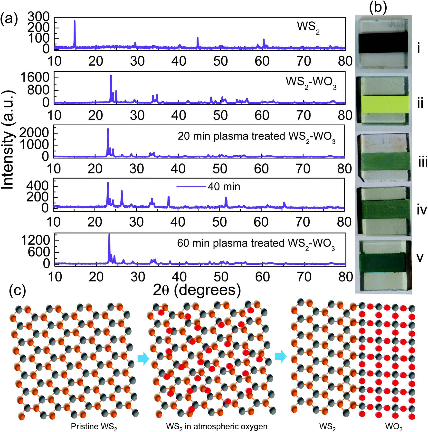 | ||
| Fig. 1 (a) XRD patterns obtained from the pristine WS2 and plasma treated samples showing the peaks corresponding to phase-pure and mixed phases. (b) Photographs show the WS2 samples in the (i) as coated pristine state, (ii) show the WS2–WO3 mixed phase sample, and (iii), (iv) and (v) are 20, 40 and 60 minutes of plasma treated WS2 respectively. (c) Illustration shows the formation of the mixed oxy-sulfide phase in WS2 upon annealing in the atmosphere. | ||
Fig. 2 shows the SEM images obtained from pristine and plasma treated dual phase WS2–WO3 samples. A significant variation was observed in the morphology of dual oxy-sulfide phase samples under pristine and plasma treated conditions. The columns are arranged according to the magnifications, while the rows are arranged based on the duration of plasma treatment. All the images were acquired at 15 kV with magnifications of 1000×, 10![[thin space (1/6-em)]](https://www.rsc.org/images/entities/char_2009.gif) 000× and 20000× to compare the change in morphology. The first row shows the surface morphology of the WS2–WO3 dual phase sample with no plasma treatment. The low magnification (1000×) image identified that the surface of the sample was not smooth but porous in nature due to the use of polyester as a binder to make the colloidal paste from phase-pure WS2 powder. The polyester was evaporated from the bulk doctor bladed WS2 sample upon 530 °C annealing and the solid film was made. Although the polyester was removed from the WS2 sample, the porosity was acquired and the surface also became rough as can be seen in the 1000× image in the first row. Further magnified images to 10000× and 20000× illustrated in the first row (second and third columns) clearly show the formation of macroscopic clusters in the shape of randomly distributed platelets. As is shown in the two higher magnified images, the shape of the platelets is not specific in terms of dimensions as well as the distribution. Surface morphology images shown in the second row of Fig. 2 represent the WS2–WO3 samples treated by plasma for 20 minutes. The lower magnified surface morphology of the 20 minute plasma treated WS2–WO3 sample shown in the second row (first column) was observed to be very similar to the untreated sample. However, it is evident that the shapes and distribution of the platelets, illustrated in the first row, are completely changed as shown in the 10000× and 20000× magnified images in the second row. It is very clear that platelets shaped into hexagons upon 20 minute plasma treatment on WS2–WO3. The surface morphology images listed in the third and fourth rows represent WS2–WO3 samples treated by plasma for 40 and 60 minutes respectively. Similar to previous observation, the 1000× magnification showed simply a porous surface morphology but the 10000× and 20000× images in both the rows assured that 40 and 60 minutes of plasma treatment on the dual WS2–WO3 phase samples made significant changes in the platelets. Increased plasma duration introduced changes in the surface morphology more effectively compared to the untreated and 20 minute treated samples. It is observed that hexagonal shapes were predominant in the case of 40 and 60 minute treated samples with sharp edges. Plasma, in this case by argon, is an ionized environment in which nanostructured functional materials and their surface become sensitive. It is expected that plasma environment interacts with unsaturated dangling bonds present in the surface of the semiconductor material and passivates them by saturating the energy. The passivation process makes the dangling bonds inactive and thus they don't participate in any charge transport processes.
000× and 20000× to compare the change in morphology. The first row shows the surface morphology of the WS2–WO3 dual phase sample with no plasma treatment. The low magnification (1000×) image identified that the surface of the sample was not smooth but porous in nature due to the use of polyester as a binder to make the colloidal paste from phase-pure WS2 powder. The polyester was evaporated from the bulk doctor bladed WS2 sample upon 530 °C annealing and the solid film was made. Although the polyester was removed from the WS2 sample, the porosity was acquired and the surface also became rough as can be seen in the 1000× image in the first row. Further magnified images to 10000× and 20000× illustrated in the first row (second and third columns) clearly show the formation of macroscopic clusters in the shape of randomly distributed platelets. As is shown in the two higher magnified images, the shape of the platelets is not specific in terms of dimensions as well as the distribution. Surface morphology images shown in the second row of Fig. 2 represent the WS2–WO3 samples treated by plasma for 20 minutes. The lower magnified surface morphology of the 20 minute plasma treated WS2–WO3 sample shown in the second row (first column) was observed to be very similar to the untreated sample. However, it is evident that the shapes and distribution of the platelets, illustrated in the first row, are completely changed as shown in the 10000× and 20000× magnified images in the second row. It is very clear that platelets shaped into hexagons upon 20 minute plasma treatment on WS2–WO3. The surface morphology images listed in the third and fourth rows represent WS2–WO3 samples treated by plasma for 40 and 60 minutes respectively. Similar to previous observation, the 1000× magnification showed simply a porous surface morphology but the 10000× and 20000× images in both the rows assured that 40 and 60 minutes of plasma treatment on the dual WS2–WO3 phase samples made significant changes in the platelets. Increased plasma duration introduced changes in the surface morphology more effectively compared to the untreated and 20 minute treated samples. It is observed that hexagonal shapes were predominant in the case of 40 and 60 minute treated samples with sharp edges. Plasma, in this case by argon, is an ionized environment in which nanostructured functional materials and their surface become sensitive. It is expected that plasma environment interacts with unsaturated dangling bonds present in the surface of the semiconductor material and passivates them by saturating the energy. The passivation process makes the dangling bonds inactive and thus they don't participate in any charge transport processes.
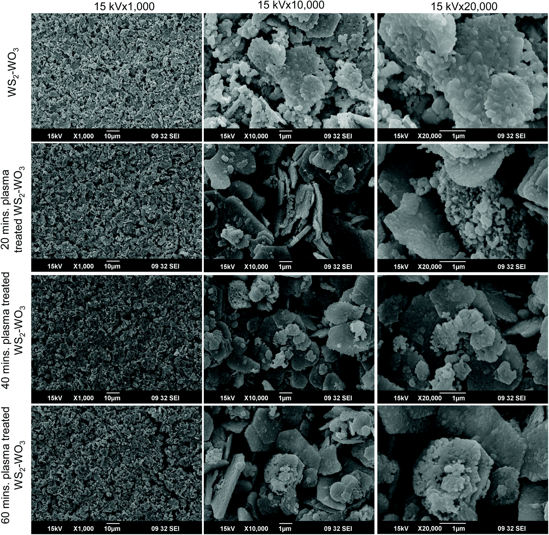 | ||
| Fig. 2 SEM images of the pristine WS2–WO3 along with plasma treated samples obtained at different magnifications showing the changes in nano-morphology. A closer comparative view of the SEM images (third column) assures the effect of plasma on the variation of morphology at the nanoscale with respect to exposure time. | ||
Fig. 3 shows the TEM images of the pristine WS2–WO3 samples in the first row along with 20 and 60 minutes of plasma treated samples in the second and third rows, respectively. The low magnification images in the first column for all three sets of samples were observed to be similar. However, as it is approached to higher magnifications, as illustrated in the second and third columns, the morphology at the nanoscale regimes exhibited significant changes as they were in the SEM images as shown in Fig. 2. Interestingly, the HRTEM images of WS2–WO3 shown in the second and third columns of the first row showed a clear and predominant grain boundary which separated two grains as illustrated. From the images, it is very obvious that there is a major difference between the two grains that is separated by the well-defined boundary. As evidenced from XRD analysis shown in Fig. 1(a), the mixed dual phase WS2–WO3 was further confirmed via the HRTEM images illustrated in Fig. 3 columns 2 and 3 for the untreated and plasma treated samples of WS2–WO3. The fourth columns in Fig. 3 shows the SAED patterns of untreated WS2–WO3, 20 and 60 minute plasma treated WS2–WO3 samples respectively. The diffraction spots observed in the SAED pattern shown in the first row (fourth column) assert the crystallinity of the WS2–WO3 dual phase samples. It is important to note that the SAED patterns shown in the second and third rows were acquired from the large area of the sample and thus the diffraction spots were not clearly visible as in the first row. It emphasized that plasma treatment interacted in the samples through the van der Waals gap and it did not affect the crystallinity much. The ionized gas species in the plasma have a tendency to diffuse into the materials if they have porosity or any form of gaps on the surface at which the interaction occurs. As the WS2–WO3 is naturally a 2D-layered material, the plasma utilized the van der Waals gap to diffuse into the bulk and thus the significant changes occurred. At the first stage, the annealing temperature caused the oxy-sulfide phase in pristine WS2, followed by the other changes shown in the HRTEM images originating from the plasma treatment at different durations.
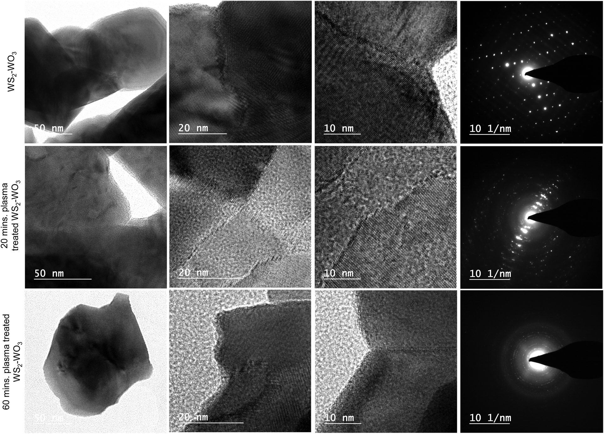 | ||
| Fig. 3 TEM images illustrating the effect of 20 and 60 minutes of plasma treatment on the WS2–WO3 sample in comparison with pristine WS2–WO3 at different magnifications along with their SAED patterns. | ||
The HRTEM image of the 20 minute plasma treated sample (shown in the second row) is isolated and shown in Fig. 4 to elucidate the sulfide and oxide grains separated by grain boundary, which looks amorphous dominated. The red arrows indicate the clearly visible grain boundary which separates the WS2 from WO3. It is also noticed that the grain boundary propagates as a phase-marker through which the phases existing in the sample can be identified. Fig. 4 shows WS2 and WO3 with d-spacing values of 0.26 nm and 0.37 nm, respectively. The image in the inset shows an illustration of the formation of the oxy-sulfide dual phase. A similar oxidation phenomenon was observed by Zhou et al. but without any grain boundary.44
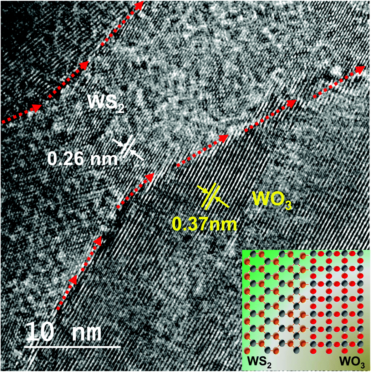 | ||
| Fig. 4 HRTEM image showing the presence of the oxy-sulfide dual phase with clear boundaries separating the phases. | ||
Fig. 5(a) shows optical absorption spectra of the WS2–WO3 sample with no plasma treatment along with the same for 20, 40 and 60 minute plasma treated samples. The measured optical absorption spectra in the spectral window of 350 nm–800 nm showed a systematic increase in the absorption with respect to the duration of plasma treatment. The untreated WS2–WO3 sample resulted in lower absorption compared to all other plasma treated samples as shown in Fig. 5(a). The duration of the plasma treatment on the WS2–WO3 samples is observed to facilitate optical absorption as the absorption increased with respect to the duration. It can be attributed to the clearance of light scattering centers on the surface of samples by plasma treatment. In general, functional materials exhibit light scattering due to various possible reasons that are associated with any imperfections in the materials and size effects. Such imperfections that are associated with the surface of WS2–WO3 were removed by plasma and this became more effective for longer duration as observed in the increase in absorption with respect to increasing the duration of plasma treatment. Furthermore, it is evident that the enhancement in optical absorption is not related to the change in the thickness of the samples as the study used samples that were coated in the same approach with consistent thickness. Fig. 5(b) shows the J–V characteristics of the solar cells fabricated using WS2–WO3 as a reference photo-electrode and further changes in the photovoltaic characteristics under the influence of plasma treatment were observed. Table 1 summarizes the photovoltaic parameters measured under the AM1.5 illumination level. The solar cell utilized 20 minute plasma treated WS2–WO3 photo-anode exhibited open circuit voltage (VOC), short circuit current density (JSC), fill factor (FF) and efficiency (η) of 450 mV, 3.3 mA cm−2, 44.3%, and 0.7%, respectively. Further increment in the duration of plasma treatment reduced all the parameters compared to the solar cell utilized untreated WS2–WO3 as a photo-anode. It suggests that there is an optimum duration of plasma treatment at which the surface and bulk of the WS2–WO3 sample become favorable for charge transport in resulting solar cells. Fig. 5(c) shows a schematic scheme to illustrate the WS2–WO3 mixed phase sample with an N719 dye molecule as a major photo-absorber. Optical absorption occurs simultaneously at both WS2–WO3 and N719 as both have optimum optical bandgap values which efficiently work in the visible spectral energy window starting from 350 nm to 800 nm. Photo-generated electrons are generated from the highest occupied molecular orbital (HOMO) to the lowest unoccupied molecular orbital (LUMO) in N719 dye, while the electrons are excited from the valence band (EV) of the WS2 to the conduction band (EC). Photo-generated electrons from both the optically active materials are injected into the EC of WO3 at which charge transport occurs to reach the FTO electrode. This situation suggests that the optical properties of WS2 and the electrical properties of WO3 become more important as they participate more effectively in photo-absorption and electron transport, respectively.
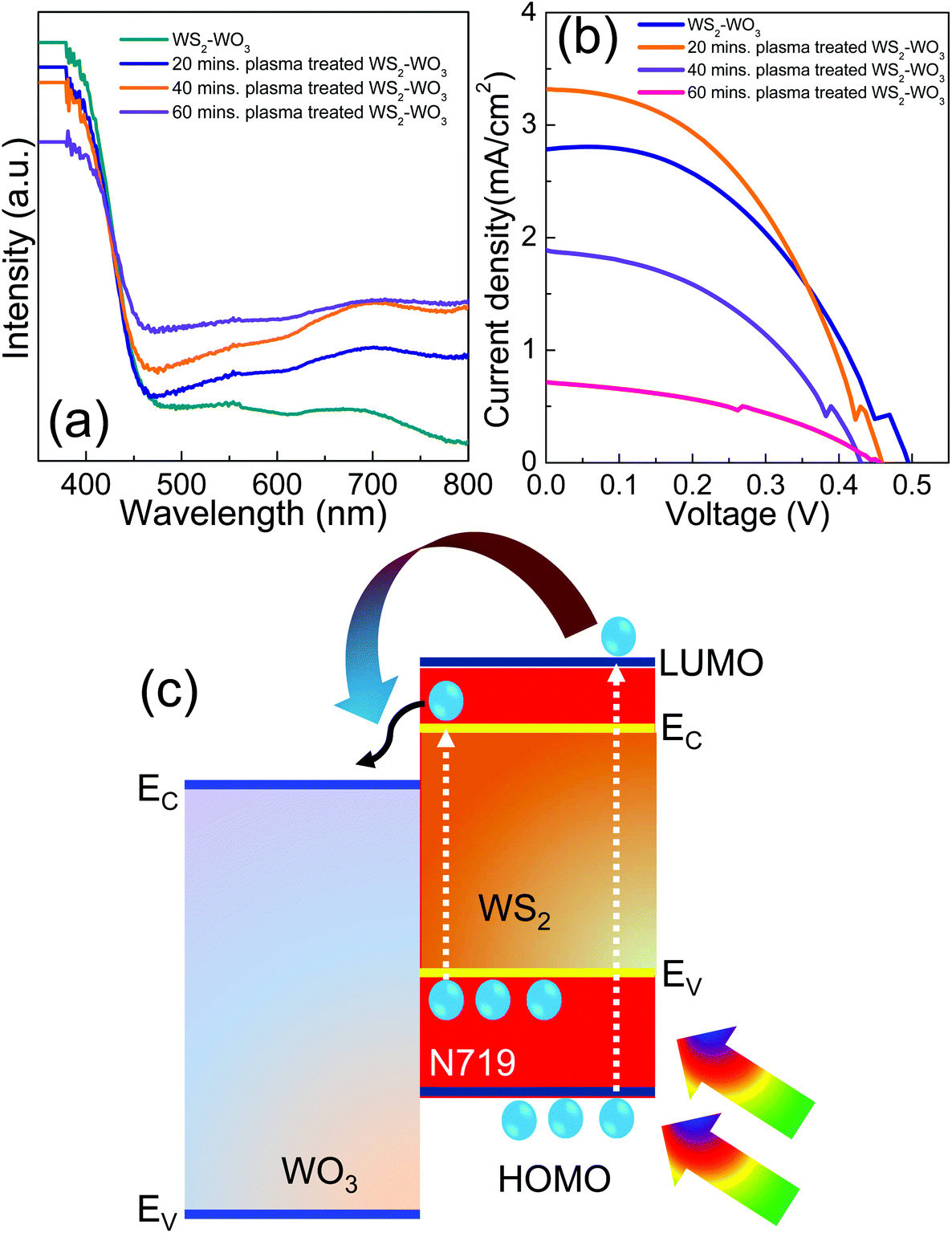 | ||
| Fig. 5 (a) UV-Visible optical absorption spectra of pristine WS2–WO3 and samples treated with plasma for 20, 40 and 60 minutes, (b) J–V characteristics of the solar cells employing the same samples as photo-anodes and (c) schematic illustration of energy band alignment at the WS2–WO3 interface with N719 dye. | ||
| Photo-anodes | V oc (mV) | J sc (mA cm−2) | FF (%) | η (%) | S.D. |
|---|---|---|---|---|---|
| WO3–WS2 | 490 | 2.8 | 44.5 | 0.6 | 0.050 |
| 20 min plasma treated | 450 | 3.3 | 44.3 | 0.7 | 0.057 |
| 40 min plasma treated | 440 | 1.9 | 42.4 | 0.4 | 0.055 |
| 60 min plasma treated | 450 | 0.7 | 41.3 | 0.1 | 0.024 |
Fig. 6 shows the (a) Nyquist and (b) Bode phase characteristics of the solar cell employed pristine WS2–WO3 and 20 minute plasma treated WS2–WO3. The semicircle obtained in the medium frequency range corresponds to the interfaces between WS2–WO3/N719/iodide/tri-iodide. It is evident that the solar cell with pristine WS2–WO3, as an electron acceptor, resulted in a much higher impedance compared with the solar cell with 20 minute plasma treated WS2–WO3. It can be attributed to the smaller amount of dye loading in the pristine WS2–WO3 sample compared to that in the 20 minute plasma treated WS2–WO3 sample. We believe that the surface of the pristine WS2–WO3 sample was much smoother compared to that of the 20 minute plasma treated WS2–WO3 sample which reduced dye adsorption. Plasma treatment increased the dye adsorption as it introduces some roughness on the surface which eventually facilitates the bonding of the dye molecules. In addition to impedance, photo-generated electron lifetime (τn) was also calculated from the EIS measurements using τn = 1/(2πf), where f is the frequency at which the highest phase shift occurs in the Bode phase characteristics. The solar cell with pristine WS2–WO3 and 20 minute plasma treated WS2–WO3 showed τn = 0.43 s and 1.14 s respectively. It is evident that increasing τn facilitates effective charge transport in solar cells and also helps effective charge collection.
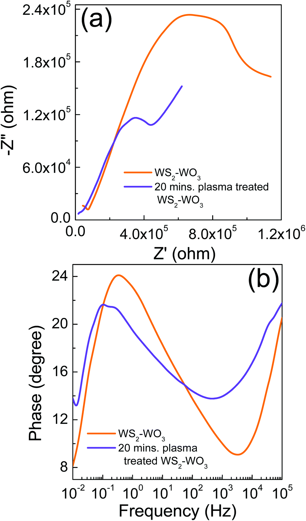 | ||
| Fig. 6 (a) Nyquist and (b) Bode phase characteristics of the solar cells employing pristine WS2–WO3 and sample treated with plasma for 20 minutes. | ||
4 Conclusions
Photovoltaic characteristics of dye sensitized dual oxy-sulfide phase WS2–WO3 samples were examined with respect to plasma treatment. It is concluded that photo-absorption in the visible spectral window can be increased using plasma treatment but achieving higher photo-current with respect to the duration of plasma treatment is rather challenging as the latter depends more on various physical processes such as photo-carrier injection, transport and collection of charge carriers that involve different materials in a solar cell.Conflicts of interest
There are no conflicts to declare.Acknowledgements
The authors thank Amrita Center for Nanosciences for providing PVD Cluster facility through industry support to perform plasma processing on functional materials for energy conversion applications. The authors also would like to thank Mr Sajin, Mr Sarath, and Ms Selvi for their help in various characterization studies.References
- S. Shalini, R. Balasundaraprabhu, T.S. Kumar, N. Prabavathy, S. Senthilarasu and S. Prasanna, Int. J. Energy Res., 2016, 40(10), 1303–1320 CrossRef CAS.
- P. Chawla and M. Tripathi, Int. J. Energy Res., 2016, 40(10), 1303–1320 CrossRef.
- M. Ye, X. Wen, M. Wang, J. Iocozzia, N. Zhang, C. Lin and Z. Lin, Mater. Today, 2015, 18(3), 155–162 CrossRef CAS.
- P. Roy, D. Kim, K. Lee, E. Spiecker and P. Schmuki, Nanoscale, 2010, 2(1), 45–59 RSC.
- S. Chappel, S. G. Chen and A. Zaban, Langmuir, 2002, 8(8), 3336–3342 CrossRef.
- J. Xu, S. Wu, J. Jin and T. Peng, Nanoscale, 2016, 8(44), 18771–18781 RSC.
- G. Kron, U. Rau, M. Dürr, T. Miteva, G. Nelles, A. Yasuda and J. H. Werner, Electrochem. Solid-State Lett., 2003, 6(6), E11–E14 CrossRef CAS.
- A. B. Martinson, J. E. McGarrah, M. O. Parpia and J. T. Hupp, Phys. Chem. Chem. Phys., 2006, 8(40), 4655–4659 RSC.
- M. Y. Song, D. K. Kim, S. M. Jo and D. Y. Kim, Synth. Met., 2005, 155(3), 635–638 CrossRef CAS.
- R. Jose, V. Thavasi and S. Ramakrishna, J. Am. Ceram. Soc., 2009, 92(2), 289–301 CrossRef CAS.
- I. Concina and A. Vomiero, Small, 2015,(15), 1744–1774 CrossRef CAS PubMed.
- J. H. Lee, N. G. Park and Y. J. Shin, Sol. Energy Mater. Sol. Cells, 2011, 95(1), 179–183 CrossRef CAS.
- Z. S. Wang, H. Kawauchi, T. Kashima and H. Arakawa, Coord. Chem. Rev., 2004, 248(13–14), 1381–1389 CrossRef CAS.
- K. M. Lee, V. Suryanarayanan and K. C. Ho, Sol. Energy Mater. Sol. Cells, 2006, 90(15), 2398–2404 CrossRef CAS.
- N. Liu, K. Lee and P. Schmuki, Electrochem. Commun., 2012, 15(1), 1–4 CrossRef CAS.
- R. T. Ako, P. Ekanayake, D. J. Young, J. Hobley, V. Chellappan, A. L. Tan, S. Gorelik, G. S. Subramanian and C. M. Lim, Appl. Surf. Sci., 2015, 351, 950–961 CrossRef CAS.
- A. R. Pascoe, L. Bourgeois, N. W. Duffy, W. Xiang and Y. B. Cheng, J. Phys. Chem. C, 2013, 117(47), 25118–25126 CrossRef CAS.
- Q. Yu, Y. Wang, Z. Yi, N. Zu, J. Zhang, M. Zhang and P. Wang, ACS Nano, 2010,(10), 6032–6038 CrossRef CAS PubMed.
- J. Bisquert, A. Zaban and P. Salvador, J. Phys. Chem. B, 2002, 106(34), 8774–8782 CrossRef CAS.
- R. Li, J. Liu, N. Cai, M. Zhang and P. Wang, J. Phys. Chem. B, 2010, 114(13), 4461–4464 CrossRef CAS PubMed.
- R. Mas-Balleste, C. Gomez-Navarro, J. Gomez-Herrero and F. Zamora, Nanoscale, 2011, 3(1), 20–30 RSC.
- K. S. Novoselov, A. Mishchenko, A. Carvalho and A. C. Neto, Science, 2016, 353(6298), aac9439 CrossRef CAS PubMed.
- M. Shanmugam, R. Jacobs-Gedrim, E. S. Song and B. Yu, Nanoscale, 2014, 6(21), 12682–12689 RSC.
- S. J. Kim, K. Choi, B. Lee, Y. Kim and B. H. Hong, Annu. Rev. Mater. Res., 2015, 45, 63–84 CrossRef CAS.
- S. C. Dhanabalan, J. S. Ponraj, H. Zhang and Q. Bao, Nanoscale, 2016, 8(12), 6410–6434 RSC.
- Y. Li, N. Dong, S. Zhang, X. Zhang, Y. Feng, K. Wang, L. Zhang and J. Wang, Laser Photonics Rev., 2015, 9(4), 427–434 CrossRef CAS.
- H. R. Gutiérrez, N. Perea-López, A. L. Elías, A. Berkdemir, B. Wang, R. Lv, F. López-Urías, V. H. Crespi, H. Terrones and M. Terrones, Nano Lett., 2012, 13(8), 3447–3454 CrossRef PubMed.
- N. Perea-López, A. L. Elías, A. Berkdemir, A. Castro-Beltran, H. R. Gutiérrez, S. Feng, R. Lv, T. Hayashi, F. López-Urías, S. Ghosh and B. Muchharla, Adv. Funct. Mater., 2013, 23(44), 5511–5517 CrossRef.
- C. Cong, J. Shang, X. Wu, B. Cao, N. Peimyoo, C. Qiu, L. Sun and T. Yu, Adv. Opt. Mater., 2014, 2(2), 131–136 CrossRef.
- Y. Sang, Z. Zhao, M. Zhao, P. Hao, Y. Leng and H. Liu, Adv. Mater., 2015, 27(2), 363–369 CrossRef CAS.
- A. S. Aji, P. Solís-Fernández, H. G. Ji, K. Fukuda and H. Ago, Adv. Funct. Mater., 2017, 27(47), 1703448 CrossRef.
- B. Mahler, V. Hoepfner, K. Liao and G. A. Ozin, J. Am. Chem. Soc., 2014, 136(40), 14121–14127 CrossRef CAS PubMed.
- E. Hossain, A. A. Rahman, R. D. Bapat, J. B. Parmar, A. P. Shah, A. Arora, R. Bratschitsch and A. Bhattacharya, Nanoscale, 2018, 10(35), 16683–16691 RSC.
- S. Cao, T. Liu, S. Hussain, W. Zeng, X. Peng and F. Pan, Mater. Lett., 2014, 129, 205–208 CrossRef CAS.
- S. Jo, J. W. Jung, J. Baik, J. W. Kang, I. K. Park, T. S. Bae, H. S. Chung and C. H. Cho, Nanoscale, 2019, 11(18), 8706–8714 RSC.
- T. Siciliano, A. Tepore, G. Micocci, A. Serra, D. Manno and E. Filippo, Sens. Actuators, B, 2008, 133, 321–326 CrossRef CAS.
- F. Wang, C. D. Valentin and G. Pacchioni, ChemCatChem, 2012, 4, 476–478 CrossRef CAS.
- H. Zheng, Y. Tachibana and K. Kalantar-zadeh, Langmuir, 2010, 26, 19148–19152 CrossRef CAS PubMed.
- A. Thangaraja, S. M. Shinde, G. Kalita and M. Tanemura, Mater. Lett., 2015, 156, 156–160 CrossRef CAS.
- A. Ennaoui, S. Fiechter, K. Ellmer, R. Scheer and K. Diesner, Thin Solid Films, 1995, 261(1–2), 124–131 CrossRef CAS.
- W. Zeng, L. P. Feng, J. Su, H. X. Pan and Z. T. Liu, J. Alloys Compd., 2018, 745, 834–839 CrossRef CAS.
- S. Jana, P. Bera, B. Chakraborty, B. C. Mitra and A. Mondal, Appl. Surf. Sci., 2014, 317, 154–159 CrossRef CAS.
- A. Azam, J. Kim, J. Park, T. G. Novak, A. P. Tiwari, S. H. Song, B. Kim and S. Jeon, Nano Lett., 2018, 18(9), 5646–5651 CrossRef CAS PubMed.
- P. Zhou, Q. Xu, H. Li, Y. Wang, B. Yan, Y. Zhou, J. Chen, J. Zhang and K. Wang, Angew. Chem., Int. Ed., 2015, 54(50), 15226–15230 CrossRef CAS PubMed.
| This journal is © The Royal Society of Chemistry 2020 |