
 Open Access Article
 This Open Access Article is licensed under a
 Creative Commons Attribution 3.0 Unported Licence
Towards the evaluation of defects in MoS2 using cryogenic photoluminescence spectroscopy†
Tim
Verhagen
 a,
Valentino L. P.
Guerra
b,
Golam
Haider
b,
Martin
Kalbac
*b and
Jana
Vejpravova
*a
a,
Valentino L. P.
Guerra
b,
Golam
Haider
b,
Martin
Kalbac
*b and
Jana
Vejpravova
*a
aDepartment of Condensed Matter Physics, Faculty of Mathematics and Physics, Charles University, Ke Karlovu 5, 121 16 Prague 2, Czech Republic. E-mail: jana@mag.mff.cuni.cz
bJ. Heyrovsky Institute of Physical Chemistry of the CAS, v.v.i., Dolejskova 2155/3, CZ-182 23 Prague 8, Czech Republic. E-mail: kalbac@jh-inst.cas.cz
First published on 13th December 2019
Abstract
Characterization of the type and density of defects in two-dimensional (2D) transition metal dichalcogenides (TMDs) is important as the nature of these defects strongly influences the electronic and optical properties of the material, especially its photoluminescence (PL). Defect characterization is not as straightforward as it is for graphene films, where the D and D′ Raman scattering modes easily indicate the density and type of defects in the graphene layer. Thus, in addition to the Raman scattering analysis, other spectroscopic techniques are necessary to perform detailed characterization of atomically thin TMD layers. We demonstrate that PL spectroscopy performed at liquid helium temperatures reveals the key fingerprints of defects in TMDs and hence provides valuable information about their origin and concentration. In our study, we address defects in chemical vapor deposition (CVD)-grown MoS2 monolayers. A significant difference is observed between the as-grown monolayers compared with the CVD-grown monolayers transferred onto a Si/SiO2 substrate, which contain extra defects due to the transfer process. We demonstrate that the temperature-dependent Raman and PL micro-spectroscopy techniques enable disentangling the contributions and locations of various defect types in TMD systems.
I. Introduction
Two-dimensional (2D) transition metal dichalcogenides (TMDs) possess extraordinary optical and electronic properties.1–3 The fundamental feature that makes this class of materials unique is the opening of a direct bandgap when at monolayer thicknesses. Extensive experimental and theoretical research has been reported that explores the strong light–matter interactions of single layer TMDs and van der Waals heterostructures that consist of stacks of single-layer TMDs and other 2D materials.4,5 This new class of hybrid materials features a great capacity for numerous optoelectronic applications that vary from light harvesting and emitting sensors6,7 and lasers8 to smart valleytronic devices.9Significant effort has been invested in the controllable growth of TMD monolayers specifically to achieve a desired monolayer quality, which has enabled electronic and optical performances similar to their exfoliated counterparts.4,5 A key parameter to be tuned with respect to the required quality is the control over the quantity and type of defects as the optical and electronic properties are directly related to the defects.10–12 Typical CVD grown and exfoliated monolayer TMD crystals have a defect density in the order of 1012 to 1013 cm−2.13,14 The actual type of defect depends on the ‘growth’ method; sulfur vacancies dominate in mined ‘natural’ MoS2 and CVD-grown films,15 whereas metal vacancies and antisites dominate in crystals grown by chemical vapour transport.16 However, the presence of defects does not represent only a disadvantage. Recent results on MoS2 based memristors showed that the bias induced dynamics of defects enables resistive switching with a varying Schottky barrier height.17
All defect types modify locally the band structure and several theoretical studies showed that the energy levels change due to these defects.13,18–20 In Fig. 1(a), a schematic energy diagram of MoS2 is shown. For non-defective MoS2, the well-known energy diagram shows the splitting of the valence band due to the strong spin–orbit coupling of the transition metal, which results in A and B excitons. The A and B excitons are the ground state (1s) of the Wannier–Mott excitons, with excited states 2s, 3s, etc. Introducing defects creates additional energy states available, where for S vacancies energy levels within the bandgap are predicted.18
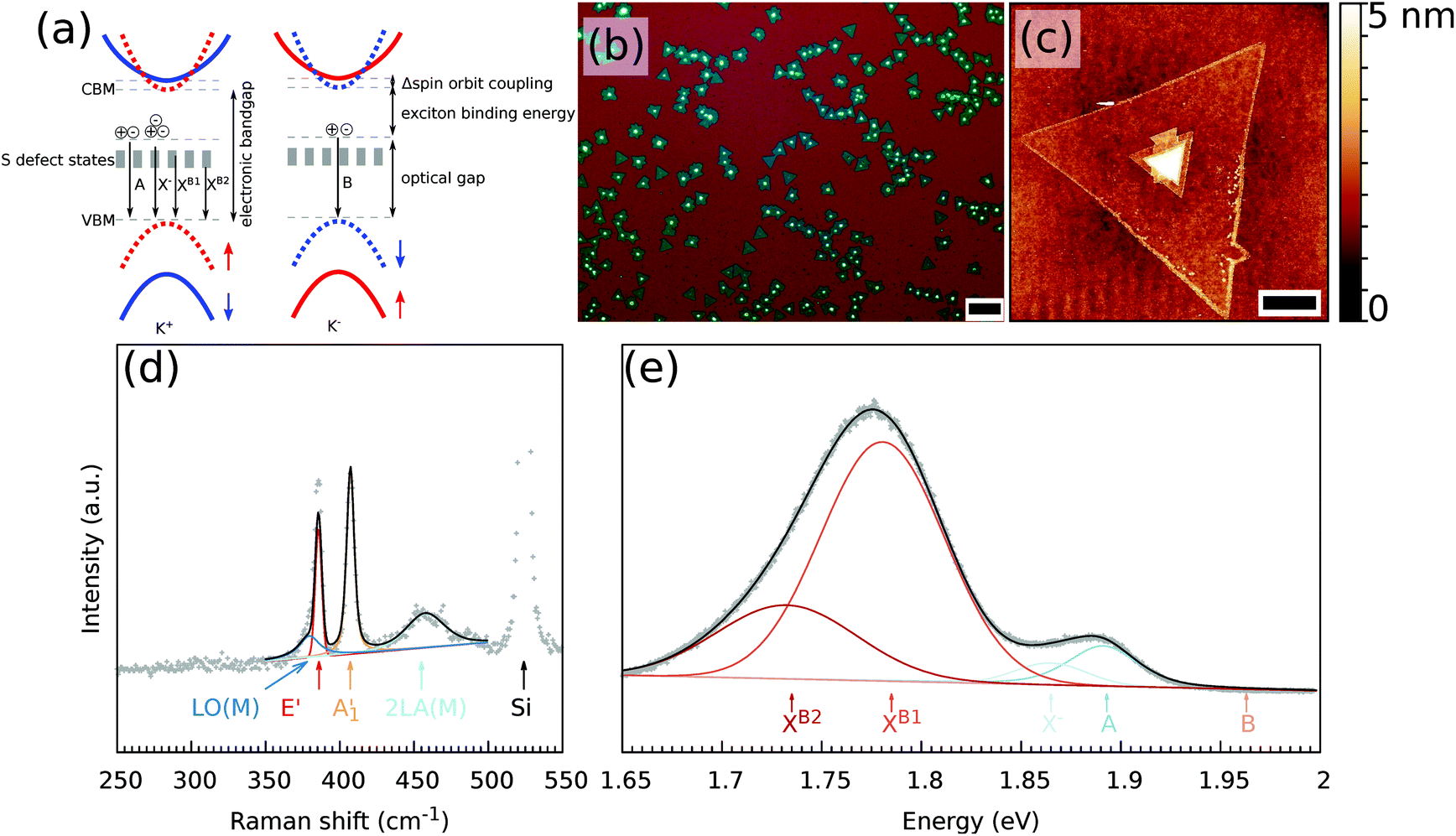 | ||
| Fig. 1 (a) Schematic band structure of MoS2. The different energy levels of the exciton and the defect states due to S vacancies are indicated. Optical (b) and AFM (c) images of the as-grown MoS2 monolayers. The white triangle seed is visible in the center of most of the monolayers from which the layer grew. Panels (d) and (e) show Raman and PL spectra of the monolayer at 10 K, with a decomposition of the different Raman modes and PL excitons, respectively. The scale bar in panels (b) and (c) is 100 μm and 5 μm, respectively. | ||
The characterization of the type and density of defects is not as straightforward as it is for graphene, where the D and D′ Raman modes are directly related to the defects in the graphene layer. For TMDs, room temperature Raman spectroscopy shows only small changes in the Raman shift with a broadening of the characteristic E′ and A′1 modes.21 Also strain and doping change22–24 the Raman modes, whereby the changes due to these effects in either the Raman shift or full-width-half maximum (FWHM) are small and difficult to disentangle. Thus, an alternative method to characterize the defect level is strongly desired.
Room temperature PL spectroscopy reveals some information about the type and density of defects, because the intensity ratio between the A and B excitons depends on the defect density.25 However, the doping and strain within the MoS2 layers strongly influence the PL signal26,27 and the defects can also enhance the PL,28 owing to the carrier confinement around defects in the TMD layers. Furthermore, the large surface-to-volume ratio of 2D materials causes the chemisorbed29 and physisorbed10 molecules to significantly influence the intrinsic properties of these materials. As an analogy to the defect-driven phenomena imprinted in the Raman-active modes, the defect-related PL modes are barely visible at room temperature and are only observable for very defective samples.28
In contrast, the low-temperature PL spectra change drastically based on the sample quality. At these temperatures, the lattice defects allow an exciton to be more strongly bound to a charged or neutral defect as well as to other quasi-particles to form a bound exciton.28 The temperature determines if the binding energy of a free exciton to a defect (Ebind) is large enough, such that the exciton can be trapped for sufficiently long time, or that the thermal energy is significantly larger and the exciton will be released before a radiative recombination occurs. A recent study on CVD-grown WS2 showed that the defects consist primarily of mono- and di-sulfur vacancies, which are mostly located on the edges of the flake.30 A vacancy at the site of a transition metal (Mo or W) also results in the creation of a quantum emitter that can emit photons with a very well-defined energy band.31
Dramatic changes in the PL spectra with temperature thus allow temperature-dependent and spatially resolved Raman and PL spectroscopy techniques to be great tools to explore the types and location of defects in TMDs.
Our work focuses on MoS2 monolayers grown via CVD. To reliably correlate the Raman and PL spectra over all temperatures, spectroscopic mapping was performed from the same flake. We also addressed the differences in the type of defect in the as-grown monolayers and those transferred to another Si/SiO2 substrate. We observed significant differences in the type of defect through the modification of the PL response, suggesting a different exciton relaxation mechanism for the as-grown and the transferred MoS2 monolayers.
II. Experimental methods
The MoS2 monolayers were grown using chemical vapor deposition (CVD) with MoO2 (Sigma Aldrich #234761) and S (Sigma Aldrich #344621) as the sources at atmospheric pressure.32,33For some experiments, the MoS2 was transferred to a different Si/SiO2 (300 nm) substrate using a wet transfer process.34
Ambient Raman and PL spectral maps were measured using a WITec Alpha300R spectrometer equipped with a piezo stage and a RayShield Coupler. Temperature dependent Raman and photoluminescence (PL) spectral maps were measured using a low temperature confocal Raman microscope insert (attoRAMAN, attocube) that was placed in a Physical Property Measurement System (PPMS, Quantum Design).
From the obtained Raman spectra, the Raman intensity, Raman shift, and FWHM were obtained by fitting pseudo-Voigt peak functions to the E′, A′1, LO(M), and 2LA(M) modes.35 From the obtained PL spectra, the PL intensity, photon energy, and photon FWHM were obtained by fitting pseudo-Voigt peak functions to the neutral A exciton X0, the charged exciton (trion, X−), the B exciton, and low temperature defect XB1 and XB2 bands.
Ambient AFM images were recorded using a Bruker Dimension Icon with ScanAssyst-air silicon nitride probes. The measurements were performed in the PeakForce tapping mode with a peak force setpoint of approximately 0.3–0.6 nN. The images were further processed using the Gwyddion software.36
For more experimental details please see the ESI.†
III. Results and discussion
The obtained MoS2 monolayers were first inspected using optical microscopy and ambient Raman and PL spectroscopy techniques. A typical optical microscope image of the grown MoS2 monolayers is shown in Fig. 1(b). When growing MoS2 using MoO2 as the precursor,33 it is possible to obtain a continuous coverage of the entire sample (1 × 3 cm2) with MoS2 monolayer triangles that are tens of micrometers large. The growth began with the nucleation of a small MoO2 crystal, which acted as a seed to grow the MoS2 layer. Depending on the exact growth conditions, such as the time of the S vapor exposure, the seeds may not be completely converted to a monolayer. A small area in the center of the monolayer can be seen in the optical and AFM images [Fig. 1(b) and (c), respectively], where the multilayer MoS2 was grown.Fig. 1(d) and (e) show the typical Raman and PL spectra of a MoS2 monolayer. Clearly visible are the characteristic E′ and A′1 modes of the MoS2. Furthermore, on the left side of the E2g mode, one can distinguish the LO(M) mode and on the right side of the A′1 mode there is the 2LA(M) mode. Monolayer and multilayer MoS2 can be easily identified from the Raman spectra due to either the difference in the Raman shift of the E′ and A′1 modes22,37 or the presence/absence of shear and breathing modes that are typical of multilayers.38 For the MoS2 flake studied, an average value of the difference of the Raman modes of the non-center region is 21 cm−1, which is a characteristic value for monolayer MoS2. A map of the difference between the Raman shift of the E′ and A′1 modes of the MoS2 flake used in this study is shown in Fig. S1(a).† In the low wavenumber range, the multilayer additionally shows shear and breathing modes, whereas the monolayer has no such modes visible for this spectral range, as can be also seen in Fig. S1(b).† The overall quality of the MoS2 monolayer can be tentatively estimated from the full width at half maximum (FWHM) of the E′ and A′1 modes, which are at approximately 4 and 5 cm−1 under ambient conditions, respectively. The FWHM of the E′ is comparable to previously reported values of 3.7–4.2 cm−1.39
The PL part of the spectrum at 10 K (Fig. 1(e)) is dominated by the XB1 and XB2 modes, which are induced by S vacancies. Furthermore, the A exciton and trion are visible, whereas no B exciton mode is present.
Both cases – as-grown MoS2 and transferred MoS2 – are discussed individually.
As-grown MoS2
The as grown samples were investigated using temperature dependent Raman and PL spectroscopy techniques. Fig. 2 shows the temperature dependency of the Raman and PL spectra for the MoS2 monolayer at the position as indicated by a black cross in Fig. 3(a). The Raman spectra did not change significantly when the flake was cooled from 300 to 10 K. Changes in the Raman shift of the E′ and A′1 modes were small, as shown in the ESI (Fig. S34).† The FWHMs of both modes were approximately 1.5 cm−1 larger than those obtained under ambient conditions outside the cryostat using a common Raman/PL microscope. Therefore this effect can be attributed to the change in the doping level to some extent40 as the atmosphere in the cryostat (5 mbar He gas) is distinct from the ambient air. Furthermore, the 2LA(M) mode became more pronounced as the sample was cooled.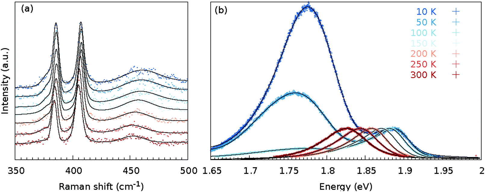 | ||
| Fig. 2 Temperature-dependent Raman (a) and PL (b) spectra at the same position of the MoS2 monolayer [as indicated in Fig. 3(a) with a cross]. The black line represents the sum of the fitted contributions for the individual modes; decomposition of the fit to the individual modes is shown in Fig. S2, S5, S8, S11, S14, S17 and S20,† whereas the black dots represent the measured data points. | ||
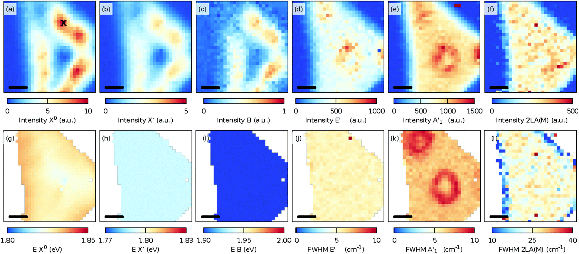 | ||
| Fig. 3 Maps of the fit intensities and energies of the neutral exciton X0 (a and g), the charged exciton (trion, X−) (b and h), and the B exciton (c and i) and the fitted intensity and FWHM of the E′ (d and j), A′1 (e and k), and 2LA(M) (f and l) Raman modes at 300 K. The scale bar in each panel is 5 μm and the ‘x’ mark in panel (a) indicates the place where the spectra in Fig. 2 were measured. | ||
In contrast, the PL spectra exhibited a significant temperature dependence [Fig. 2(b)]. At 300 K, the PL spectrum showed a clear contribution of the X0 exciton and a minor contribution of the trion and B exciton (see Fig. S2† for a fit of the individual components). As the MoS2 flake was cooled to 100 K, the contributions from the bound excitons XB1 and XB2 appeared (see Fig. S14† for a fit of the individual modes). The intensity of the defect-induced excitons increased dramatically when the temperature decreased to 10 K and became significantly larger than the contributions of the neutral X0 and B excitons or the trion (see Fig. S20† for a fit of the individual components). The dramatic increase of the XB1 and XB2 intensity can be tentatively explained by reduced interaction with phonons. In general, the phonons are scattered on defects; hence the non-radiative pathways dominate. However, when the temperature is decreased, the phonon states are less populated. Consequently non radiative pathways are less probable and the radiative pathway starts to dominate. The intensity of the XB1 and XB2 bands is finally larger than X0 as the energy of the states is lower than for X0. Note that the intensity of the X0 remains constant as the temperature decreases because the interaction of the exciton and phonons is weak.
In Fig. 3, the spatial distribution of the intensity and FWHM for the E′ [Fig. 3(d, j), Fig. 3 A′1 (e, k)], and 2LA(M) [Fig. 3(f and l)] modes is shown. A slightly larger intensity for both modes in the center and in the top corner of the flake was observed. The increased intensity is caused by the presence of multilayer MoS2 at these locations. Interestingly, the spatial distribution for the FWHM of the E′ [Fig. 3(j)] mode was quite homogeneous, whereas the FWHM of the A′1 [Fig. 3(k)] mode showed spatially confined enhancements due to the presence of the multilayer MoS2. Finally, the intensity of the 2LA(M) [Fig. 3(f)] indicates the presence of defects and has a rather homogeneous appearance.35
The intensity of the PL spectra [Fig. 3(a–c)] showed another trend. A significant PL peak was observed in defined lines parallel to the edges of the 2D crystal. At 300 K, no clear correlation was present between the variations in the PL intensity and the Raman shift, intensity, and FWHM of the measured Raman modes.
At 50 K, the PL spectrum for the MoS2 monolayer changed dramatically due to the presence of bound excitons XB1 and XB1. The spatial distribution of the intensity and photon energies of the excitons is shown in Fig. 4(a–d) and (f–i). The intensity distributions of the excitons and trion are the same as those observed at 300 K. The intensity distribution of the bound exciton XB1 is the same as for the exciton and trion. However, the intensity distribution of the XB2 exciton was much more localized and the highest intensity is present between the center and the edges and also it decreases at the corners of the MoS2 triangle. It is assumed that in the center of the sample the exciton is quenched by the presence of an ad-layer, while at the edge of the grain (flake) the sulfur vacancies are more likely passivated by oxygen. The conclusion is corroborated by recent tip-enhanced Raman spectroscopy, which revealed oxygen containing structures located systematically at the grain edges.41
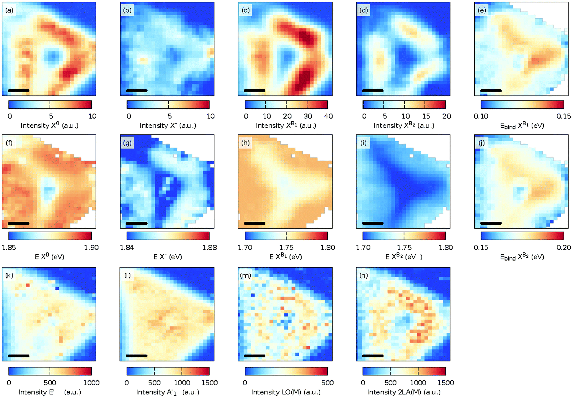 | ||
| Fig. 4 Maps of the fitted intensity (first row) and photon energy E (second row) of the neutral exciton X0 (a and f), the charged exciton (trion, X−) (b and g), and the low temperature defect modes XB1 (c and h) and XB2 (d and i). The panels (e and j) correspond to the spatial dependence of the binding energy Ebind of the XB1 and XB2 defect modes. The third row shows the fitted intensity of the E′ (k), A′1 (l), LO(M) (m), and 2LA(M) (n) Raman modes at 50 K. The scale bar in each panel is 5 μm. | ||
The binding energy of the bound exciton is defined as the energy difference between the neutral exciton and the bound exciton, Ebind as XBi = EX0 − EXBi, i = 1 or 2. Fig. 4(e) and (j) show the binding energy of both bound excitons, with median binding energies of 120 and 170 meV for the Ebind XB1 and Ebind XB2, respectively. The binding energies of the defect bound excitons agree with the previously found values of the V 1s and V 2s defects in exfoliated MoS2![[thin space (1/6-em)]](https://www.rsc.org/images/entities/char_2009.gif) 42 and are slightly smaller than the values calculated with density functional theory using the Perdew–Burke–Ernzerhof functional.18
42 and are slightly smaller than the values calculated with density functional theory using the Perdew–Burke–Ernzerhof functional.18
The intensity of the E′ and A′1 Raman modes [Fig. 4(k) and (l)] at 50 K shows the same variations as the 300 K sample, but the intensity distribution of the 2LA(M) mode at 50 K [Fig. 4(n)] closely follows the maximum intensity of the PL. Furthermore, as also shown in Fig. 2 [see Fig. S2 and S20† for a fit of the individual modes at 300 K and 10 K], the LO(M) mode,35 which is located as the shoulder of the E′ mode, became more pronounced as the sample was cooled. The spatial distribution of this mode [Fig. 4(m)] follows the same distribution as the other disorder-activated 2LA(M) modes [Fig. 4(n)].
Transferred CVD-grown MoS2
The CVD-grown MoS2 was transferred to another SiO2/Si substrate using the previously described wet transfer method. Fig. 5(a) shows the AFM image of a transferred flake. No significant changes in the topography are visible due to the potential introduction of wrinkles. Some polymer residuals are visible on both the MoS2 flake and the substrate. The Raman and PL spectra of the transferred CVD-grown MoS2 flake are shown in Fig. 5(c) and (d). It can be observed that the Raman spectrum does not possess any significant changes compared to that of the CVD grown MoS2 monolayer without transfer. However, if the Raman shift of the A′1 mode is plotted versus the Raman shift of the E′ mode, there is a significant shift visible for the E′ mode, as shown in Fig. 5(b). To estimate the influence of strain and doping, the data are plotted in the strain-doping coordinate system,22 with as origin the center of the grown data. For the influence of the strain, the used Grüneisen parameters are 0.86 and 0.15 for the E′ and A′1 modes, respectively.22 To model the influence of the doping, a shift rate with a carrier concentration of −0.33 × 10⁻¹³ cm−2 and −2.22 × 10⁻¹³ cm−2 was used for the E′ and A′1 modes, respectively.22 The contribution of defects to the Raman shift is not included in this correlation analysis.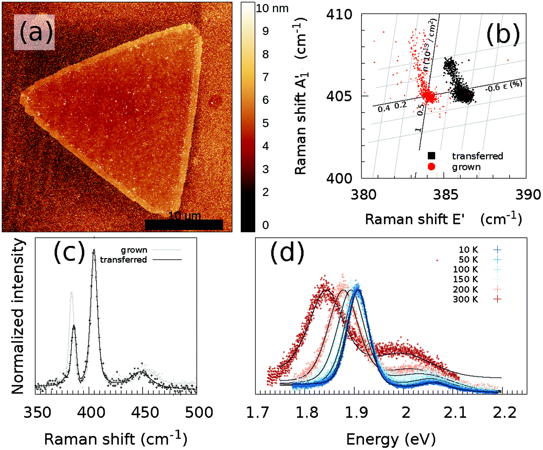 | ||
| Fig. 5 (a) AFM images of the transferred MoS2 flake. The scale bar is 10 μm. (b) Correlation between the fitted Raman shift of the A′1 and E′ modes of the transferred and grown MoS2 crystals, taking only into account the influence of strain ε and doping n at 300 K. Temperature-dependent (c) Raman and (d) PL spectra at the same position of the MoS2 monolayer. As a comparison, also the Raman spectrum of the CVD grown MoS2 monolayer from Fig. 1(d) is shown (grey line/dots). The black/grey line represents the sum of the fitted contributions of the individual modes; decomposition of the fit to the individual modes is shown in Fig. S23, S24, S26, S28, S30 and S32,† whereas the black/grey dots are the measured data points. | ||
If we now assume that the observed Raman shift between the grown and transferred samples is mostly caused by the introduction of defects during the transfer, which can result in a change of the E′ Raman shift, then a shift of approximately 2 cm−1 corresponds to the addition of 1% S vacancies.21 Furthermore, any significant damage of the sample topography, in particular formation of wrinkles introducing non-homogeneous strain, has been observed by AFM (Fig. 1c). This observation supports the conclusion that the change in sulfur vacancy concentration is the most important factor influencing the PL spectra.
The two points of clouds from both the transferred and grown samples stem from the monolayer and the multilayer areas in the center of the flake. However, also a changed doping and strain landscape play a role in the modified correlation between the A′1 and E′ modes, as will be discussed below.
The PL spectrum shows different behaviors compared to those observed for the as-grown MoS2. While the B exciton is nearly invisible in the PL spectrum of the as-grown MoS2, the B exciton is clearly visible in the transferred MoS2 and it is also shifted to higher energy. The increase of the intensity can be attributed to the doping caused by KOH. This is consistent with previous observation.45 The reason for the higher energy of the exciton is not completely clear.
Furthermore, at lower temperatures, the ratio of the intensities between the A and B excitons increased. However, no XB1 and/or XB2 PL peak appeared down to the lowest measured temperatures.
Fig. 6 shows the spatial distributions of the fit intensity and energy of the X0 (a, d), X− (b, e), and B (c, f) excitons at 50 K. The PL intensity is more homogeneous except at the center of the crystal because of the presence of the thicker seed-crystal. The spatial variations in the energy suggest that the strain was released from the transfer, and/or another strain distribution was induced in the sample, which can be understood as follows. During the CVD growth of TMDs, the strain was induced in the crystals as the sample was cooled to room temperature after its growth at higher temperatures due to the different thermal expansion coefficients of the substrate and the TMD layer. When the substrate was etched during the transfer, the strain in the crystals was partly removed or redistributed.43 Assuming now that the observed Raman shifts in Fig. 5(b) are solely due to a change in strain and doping, a maximum change in strain of approximately −0.3% relative to the strain in the grown sample and a maximum change in doping of approximately 0.2 × 1013 cm−2 relative to the grown sample can be expected. However, the variations in strain are smaller as the induced defects influence the Raman shift of mostly the E′ mode.
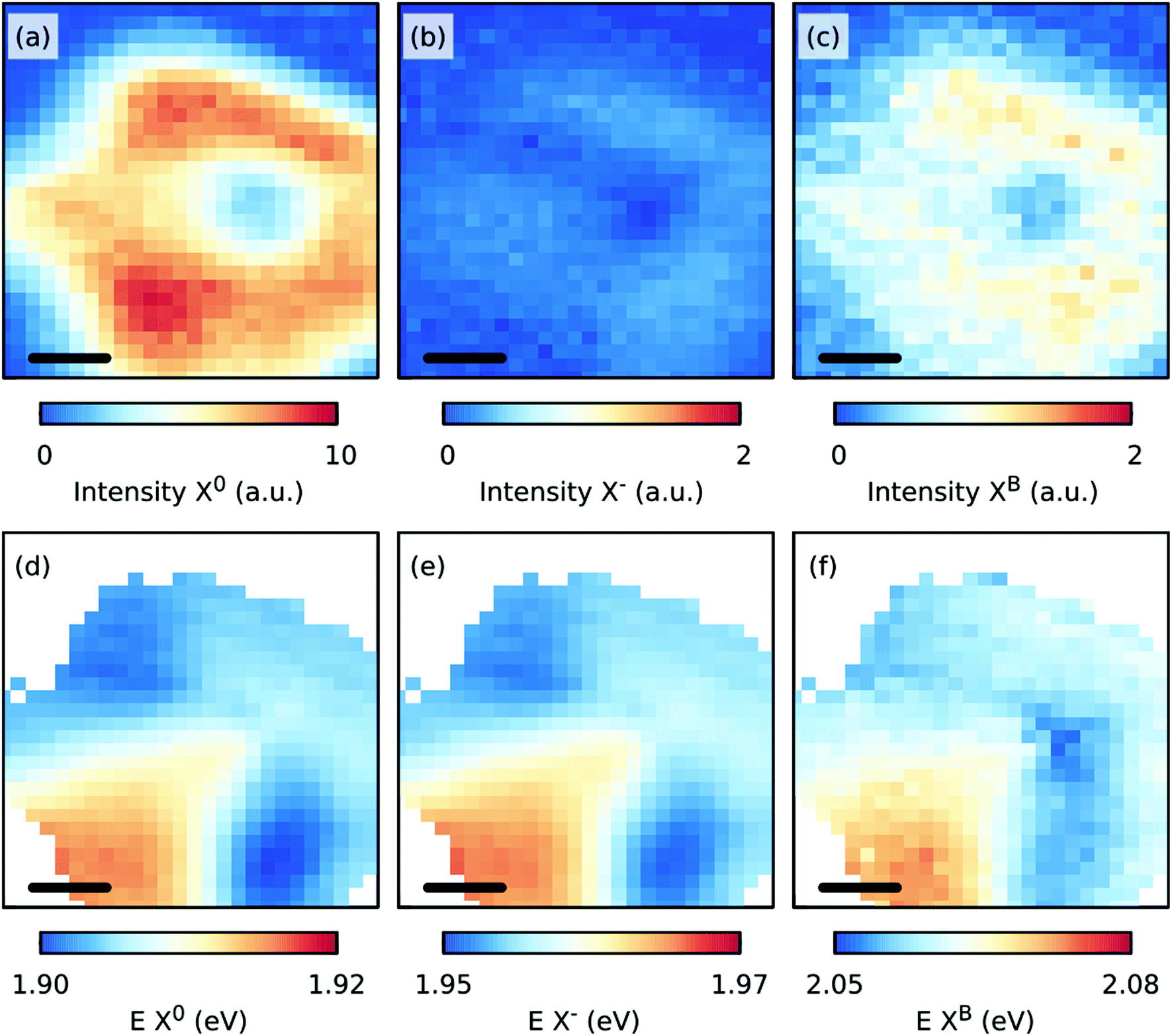 | ||
| Fig. 6 Maps of the fit intensities (a–c) and energies, E (d–f) of the X0, X−, and B excitons for the transferred, CVD grown MoS2 monolayer at 50 K. The scale bar in each panel is 5 μm. | ||
The S-vacancies play an important role in the PL intensity,44 as shown in Fig. 4(a) and (c). The intensity of the PL is maximized when the intensity of either the Raman defect modes 2LA(M) or LO(M) or the defect induced PL XB1 is the largest. We suspect that the increased intensity of the 2LA(M) and LO(M) modes is related to the increased defect related PL due to the strong phonon-exciton coupling.46
The variations in the density of S-vacancies originate from the CVD growth due to moderate variations in the S-vacancy concentrations, as was shown before for the CVD-grown WS2.44
After transferring the MoS2 flakes to another Si/SiO2 substrate, no XB1 and XB2 defect modes were visible. For these samples, a significant increase in the intensity of the B mode was measured, which suggests that the defect density in the MoS2 crystal increased significantly25,47 during the transfer. The obvious question is which type of defect is created during KOH etching. Classifying the nature of defects using chemical means is rather inconsistent. However, Mo vacancies should result in the creation of quantum emitters31 and S vacancies should contribute to the creation of bound defect states. As no signature of quantum emitters was observed one can exclude the Mo vacancies. The S-vacancies are assumed to be a reason for XB1 and XB2 bands in the PL. As those bands are not present any more after the transfer one can assume that the S-vacancies are passivated during the transfer. We suggest that in the as grown MoS2 sample the vacancies are protected and/or stabilized by the underlying substrate. By the transfer procedure they are exposed to transfer the polymer and aggressive KOH environment and thus they can be passivated. The transfer remnants could passivate the S vacancies, as was shown before for exfoliated MoS2 samples covered with either Al2O3 or HfO2. Nevertheless, they would not passivate the S-vacancies in between MoS2 and the substrate. Therefore we assume that the S-vacancies are passivated by treatment with KOH, which results in oxygen termination. This is furthermore consistent with previous theoretical work, which suggested that the oxygen passivation of the S-vacancies does not lead to localized states.48 We also assume that overall density of defects strongly increases after treatment with KOH, which leads to the decrease of the total PL intensity.
The large differences in the PL spectra for the as-grown and transferred MoS2 are better explained by considering the lifetime of the excitons.25 Assuming that defects are introduced during the transfer process, the transferred samples have more defects. As the defects introduce nonradiative pathways to annihilate excitons, the total PL intensity decreases in proportion with the defect density. The radiative lifetimes of the A and B excitons are approximately 800 and 1 ps, respectively, whereas the nonradiative recombination time is approximately 10 ps. The total recombination time of the excitations in the case of the nonradiative recombination significantly decreases the recombination time of the A exciton, resulting in a significantly reduced PL intensity. However, the influence on the recombination time of the B exciton is small due to its much shorter radiative lifetime; thus, its PL intensity is not significantly changed.
IV. Conclusions
Well-defined monolayers of MoS2 were grown using CVD on SiO2/Si using MoO2 as a precursor. We transferred some of the monolayers onto another SiO2/Si substrate using a standard wet protocol and investigated the lattice and optical responses by Raman and PL spectroscopy given a ∼1 μm spatial resolution. We further generated temperature-dependent PL and Raman spectroscopy mappings of the as-grown and transferred MoS2. For the as-grown sample, the Raman spectral mappings revealed a homogeneous spatial distribution and very moderate temperature dependence, whereas there were significant spatial and thermal variations within the PL spectral maps. In general, the signal from the defect-induced excitons increased dramatically when cooling and dominated the spectra over the X0, B, and trion contributions. In the cryogenic regime, the spatial distribution of the 2LA(M) Raman mode, generally used as a measurement for defects, coincided well with the spatial distribution of the PL signal due to the XB1, X0, and trion. In contrast, the XB2 PL signal dominated at the center of the flake edges. After the transfer, the B exciton dominated the PL spectra while the defect-induced PL was negligible. This observation is consistent with the fact that an overall larger transfer-induced defect density stimulates the nonradiative pathways for exciton annihilation.We unambiguously demonstrated that the transfer process plays a significant role in the formation and location of defects in MoS2. The relaxation mechanisms of the excitons at different positions on the monolayer can be rigorously evaluated using cryogenic PL spectroscopy. Our study thus provides a reliable protocol to investigate lattice perturbations in TMDs monolayers as well as in TMD-based heterostructures and superlattices.
Conflicts of interest
There are no conflicts to declare.Acknowledgements
This research was funded by the European Research Council (ERC-Stg-716265) and the Czech Science Foundation (18-20357S). The low temperature experiments were conducted with the support of MGML infrastructure, financed by the MEYS (LM2018096). The authors acknowledge the assistance provided by the Research Infrastructures NanoEnviCz (Project No. LM2015073) supported by the Ministry of Education, Youth and Sports of the Czech Republic, and the project Pro-NanoEnviCz (Reg. No. CZ.02.1.01/0.0/0.0/16_013/0001821) supported by the Ministry of Education, Youth and Sports of the Czech Republic, and the European Union – European Structural and Investments Funds in the frame of Operational Programme Research Development and Education.References
- K. F. Mak, C. Lee, J. Hone, J. Shan and T. F. Heinz, Phys. Rev. Lett., 2010, 105, 136805, DOI:10.1103/physrevlett.105.136805
.
- A. Splendiani, L. Sun, Y. Zhang, T. Li, J. Kim, C.-Y. Chim, G. Galli and F. Wang, Nano Lett., 2010, 10, 1271, DOI:10.1021/nl903868w
- K. F. Mak, C. Lee, J. Hone, J. Shan and T. F. Heinz, Phys. Rev. Lett., 2010, 105, 136805, DOI:10.1103/PhysRevLett.105.136805
- Z. Lin, A. McCreary, N. Briggs, S. Subramanian, K. Zhang, Y. Sun, X. Li, N. J. Borys, H. Yuan, S. K. Fullerton-Shirey, A. Chernikov, H. Zhao, S. McDonnell, A. M. Lindenberg, K. Xiao, B. J. LeRoy, M. Drndic, J. C. M. Hwang, J. Park, M. Chhowalla, R. E. Schaak, A. Javey, M. C. Hersam, J. Robinson and M. Terrones, 2D Mater., 2016, 3, 042001, DOI:10.1088/2053-1583/3/4/042001
- W. Choi, N. Choudhary, G. H. Han, J. Park, D. Akinwande and Y. H. Lee, Mater. Today, 2017, 20, 116, DOI:10.1016/j.mattod.2016.10.002
- O. Lopez-Sanchez, D. Lembke, M. Kayci, A. Radenovic and A. Kis, Nat. Nanotechnol., 2013, 8, 497, DOI:10.1038/nnano.2013.100
- O. Lopez-Sanchez, E. Alarcon Llado, V. Koman, A. Fontcuberta i Morral, A. Radenovic and A. Kis, ACS Nano, 2014, 8, 3042, DOI:10.1021/nn500480u
- S. Wu, S. Buckley, J. R. Schaibley, L. Feng, J. Yan, D. G. Mandrus, F. Hatami, W. Yao, J. Vuckovic, A. Majumdar and X. Xu, Nature, 2015, 520, 69, DOI:10.1038/nature14290
- K. F. Mak, K. He, J. Shan and T. F. Heinz, Nat. Nanotechnol., 2012, 7, 494, DOI:10.1038/NNANO.2012.96
- S. Tongay, J. Suh, C. Ataca, W. Fan, A. Luce, J. S. Kang, J. Liu, C. Ko, R. Raghunathanan, J. Zhou, F. Ogletree, J. Li, J. C. Grossman and J. Wu, Sci. Rep., 2013, 3, 2657, DOI:10.1038/srep02657
- S. Yuan, R. Roldán, M. I. Katsnelson and F. Guinea, Phys. Rev. B: Condens. Matter Mater. Phys., 2014, 90, 041402(R), DOI:10.1103/PhysRevB.90.041402
- P. K. Chow, R. B. Jacobs-Gedrim, J. Gao, T.-M. Lu, B. Yu, H. Terrones and N. Koratkar, ACS Nano, 2015, 9, 1520, DOI:10.1021/nn5073495
- D. Rhodes, S. H. Chae, R. Ribeiro-Palau and J. Hone, Nat. Mater., 2019, 18, 541, DOI:10.1038/s41563-019-0366-8
- S. Shree, A. George, T. Lehnert, C. Neumann, M. Benelajla, C. Robert, X. Marie, K. Watanabe, T. Taniguchi, U. Kaiser, B. Urbaszek and A. Turchanin, 2019, arXiv:1907.03342v1.
- P. Vancsó, G. Z. Magda, J. Pető, J.-Y. Noh, Y.-S. Kim, C. Hwang, L. P. Biró and L. Tapasztó, Sci. Rep., 2016, 6, 29726, DOI:10.1038/srep29726
- D. Edelberg, D. Rhodes, A. Kerelsky, B. Kim, J. Wang, A. Zangiabadi, C. Kim, A. Abhinandan, J. Ardelean, M. Scully, D. Scullion, L. Embon, I. Zhang, R. Zu, E. J. G. Santos, L. Balicas, C. Marianetti, K. Barmak, X.-Y. Zhu, J. Hone and A. N. Pasupathy, arXiv:1805.00127v1, 2018.
- V. K. Sangwan, H.-S. Lee, H. Bergeron, I. Balla, M. E. Beck, K.-S. Chen and M. C. Hersam, Nature, 2018, 554, 500, DOI:10.1038/nature25747
- H.-P. Komsa and A. V. Krasheninnikov, Phys. Rev. B: Condens. Matter Mater. Phys., 2015, 91, 125304, DOI:10.1103/PhysRevB.91.125304
- S. Haldar, H. Vovusha, M. K. Yadav, O. Eriksson and B. Sanyal, Phys. Rev. B: Condens. Matter Mater. Phys., 2015, 92, 235408, DOI:10.1103/PhysRevB.92.235408
- G. Wang, A. Chernikov, M. M. Glazov, T. F. Heinz, X. Marie, T. Amand and B. Urbaszek, Rev. Mod. Phys., 2018, 90, 021001, DOI:10.1103/RevModPhys.90.021001
- W. M. Parkin, A. Balan, L. Liang, P. M. Das, M. Lamparski, C. H. Naylor, J. A. Rodríguez-Manzo, A. T. Charlie Johnson, V. Meunier and M. Drndić, ACS Nano, 2016, 10, 4134, DOI:10.1021/acsnano.5b07388
- A. Michail, N. Delikoukos, J. Parthenios, C. Galiotis and K. Papagelis, Appl. Phys. Lett., 2016, 108, 173102, DOI:10.1063/1.4948357
- H. J. Conley, B. Wang, J. I. Ziegler, R. F. Haglund Jr., S. T. Pantelides and K. I. Bolotin, Nano Lett., 2013, 13, 3626, DOI:10.1021/nl4014748
- B. Chakraborty, A. Bera, D. V. S. Muthu, S. Bhowmick, U. V. Waghmare and A. K. Sood, Phys. Rev. B: Condens. Matter Mater. Phys., 2012, 85, 161403(R), DOI:10.1103/PhysRevB.85.161403
- K. M. McCreary, A. T. Hanbicki, S. V. Sivaram and B. T. Jonker, APL Mater., 2018, 6, 111106, DOI:10.1063/1.5053699
- J. Conley, B. Wang, J. I. Ziegler, R. F. Haglund Jr., S. T. Pantelides and K. I. Bolotin, Nano Lett., 2013, 13, 3626, DOI:10.1021/nl4014748
- K. F. Mak, K. He, C. Lee, G. H. Lee, J. Hone, T. F. Heinz and J. Shan, Nat. Mater., 2013, 12, 207, DOI:10.1038/nmat3505
- J. Klein, A. Kuc, A. Nolinder, M. Altzschner, J. Wierzbowski, F. Sigger, F. Kreupl, J. J. Finley, U. Wurstbauer, A. W. Holleitner and M. Kaniber, 2D Mater., 2018, 5, 011007, DOI:10.1088/2053-1583/aa9642
- H. Nan, Z. Wang, W. Wang, Z. Liang, Y. Lu, Q. Chen, D. He, P. Tan, F. Miao, X. Wang, J. Wang and Z. Ni, ACS Nano, 2014, 8, 5738, DOI:10.1021/nn500532f
- V. Carozo, Y. Wang, K. Fujisawa, B. R. Carvalho, A. McCreary, S. Feng, Z. Lin, C. Zhou, N. Perea-López, A. L. Elías, B. Kabius, V. H. Crespi and M. Terrones, Sci. Adv., 2017, 3, e160281, DOI:10.1126/sciadv.1602813
- J. Klein, M. Lorke, M. Florian, F. Sigger, L. Sigl, S. Rey, J. Wierzbowski, J. Cerne, K. Müller, E. Mitterreiter, P. Zimmermann, T. Taniguchi, K. Watanabe, U. Wurstbauer, M. Kaniber, M. Knap, R. Schmidt, J. J. Finley and A. W. Holleitner, Nat. Commun., 2019, 10, 2755, DOI:10.1038/s41467-019-10632-z
- Y. Xie, Z. Wang, Y. Zhan, P. Zhang, R. Wu, T. Jiang, S. Wu, H. Wang, Y. Zhao, T. Nan and X. Ma, Nanotechnology, 2017, 28, 084001, DOI:10.1088/1361-6528/aa5439
- I. Bilgin, F. Liu, A. Vargas, A. Winchester, M. K. L. Man, M. Upmanyu, K. M. Dani, G. Gupta, S. Talapatra, A. D. Mohite and S. Kar, ACS Nano, 2015, 9, 8822, DOI:10.1021/acsnano.5b02019
- Y.-C. Lin, W. Zhang, J.-K. Huang, K.-K. Liu, Y.-H. Lee, C.-T. Liang, C.-W. Chu and L.-J. Li, Nanoscale, 2012, 4, 6637, 10.1039/C2NR31833D
- S. Mignuzzi, A. J. Pollard, N. Bonini, B. Brennan, I. S. Gilmore, M. A. Pimenta, D. Richards and D. Roy, Phys. Rev. B: Condens. Matter Mater. Phys., 2015, 91, 195411, DOI:10.1103/PhysRevB.91.195411
- D. Necas and P. Klapetek, Cent. Eur. J. Phys., 2012, 10, 181, DOI:10.2478/s11534-011-0096-2
- S. Kataria, S. Wagner, T. Cusati, A. Fortunelli, G. Iannaccone, H. Pandey, G. Fiori and M. C. Lemme, Adv. Mater. Interfaces, 2017, 4, 1700031, DOI:10.1002/admi.201700031
- X. Zhang, W. P. Han, J. B. Wu, S. Milana, Y. Lu, Q. Q. Li, A. C. Ferrari and P. H. Tan, Phys. Rev. B: Condens. Matter Mater. Phys., 2013, 87, 115413, DOI:10.1103/PhysRevB.87.115413
- Y. Yu, C. Li, Y. Liu, L. Su, Y. Zhang and L. Cao, Sci. Rep., 2013, 3, 1866, DOI:10.1038/srep01866
- S. Tongay, J. Zhou, C. Ataca, J. Liu, J. S. Kang, T. S. Matthews, L. You, J. Li, J. C. Grossman and J. Wu, Nano Lett., 2013, 13, 2831, DOI:10.1021/nl4011172
- A. Rodriguez, T. Verhagen, M. Kalbac, J. Vejpravova and O. Frank, Phys. Status Solidi RRL, 2019, 1900381, DOI:10.1002/pssr.201900381
- N. Saigala and S. Ghosh, Appl. Phys. Lett., 2016, 109, 122105, DOI:10.1063/1.4963133
- T. Hallam, N. C. Berner, C. Yim and G. S. Duesberg, Adv. Mater. Interfaces, 2014, 6, 2196, DOI:10.1002/admi.201400115
- N. Peimyoo, J. Shang, C. Cong, X. Shen, X. Wu, E. K. L. Yeow and T. Yu, ACS Nano, 2013, 7, 10985, DOI:10.1021/nn4046002
- S. Dubey, S. Lisi, G. Nayak, F. Herziger, V.-D. Nguyen, T. Le Quang, V. Cherkez, C. González, Y. J. Dappe, K. Watanabe, T. Taniguchi, L. Magaud, P. Mallet, J.-Y. Veuillen, R. Arenal, L. Marty, J. Renard, N. Bendiab, J. Coraux and V. Bouchiat, ACS Nano, 2017, 11, 11206–11216, DOI:10.1021/acsnano.7b05520
- Q. H. Tan, Y.-J. Sun, X.-L. Liu, Y. Zhao, Q. Xiong, P.-H. Tan and J. Zhang, 2D Mater., 2017, 4, 031007, DOI:10.1088/2053-1583/aa79bb
- M. Amani, M. L. Chin, A. L. Mazzoni, R. A. Burke, S. N. Pulickel, M. Ajayan, J. Lou and M. Dubey, Appl. Phys. Lett., 2014, 104, 203506, DOI:10.1063/1.4873680
- H.-P. Komsa, J. Kotakoski, S. Kurasch, O. Lehtinen, U. Kaiser and A. V. Krasheninnikov, Phys. Rev. Lett., 2012, 109, 035503, DOI:PhysRevLett.109.035503
Footnote |
| † Electronic supplementary information (ESI) available: Additional details on the Raman and PL spectroscopies, decomposition of the Raman and PL spectra, and maps of the Raman and PL spectral parameters at different temperatures for the as-grown and transferred CVD MoS2. See DOI: 10.1039/c9nr07246b |
| This journal is © The Royal Society of Chemistry 2020 |