
A closer look at the defects and luminescence of nanocrystalline fluorides synthesized via ionic liquids: the case of Ce3+-doped BaF2†
Rahul Kumar
Sharma
 a,
Yogendra Nath
Chouryal
a,
Anatoly I.
Slesarev
b,
Konstantin V.
Ivanovskikh
*b,
Ivan I.
Leonidov
cd,
Sandeep
Nigam
e and
Pushpal
Ghosh
*a
a,
Yogendra Nath
Chouryal
a,
Anatoly I.
Slesarev
b,
Konstantin V.
Ivanovskikh
*b,
Ivan I.
Leonidov
cd,
Sandeep
Nigam
e and
Pushpal
Ghosh
*a
aSchool of Chemical Sciences and Technology, Department of Chemistry, Dr H. S. Gour University (A Central University), Sagar 470003, Madhya Pradesh, India. E-mail: pushpalghosh27@gmail.com
bInstitute of Physics and Technology, Ural Federal University, Ekaterinburg 620002, Russia
cSchool of Engineering, Ural Federal University, Ekaterinburg 620002, Russia
dInstitute of High-Temperature Electrochemistry, UB RAS, Ekaterinburg 620137, Russia
eChemistry Division, Bhabha Atomic Research Centre, Trombay, Mumbai 400085, India
First published on 25th November 2019
Abstract
Phase pure BaF2 doped with Ce3+ (0.1%) nanocrystals are synthesized using an ionic liquid (IL) ([C4mim][BF4]) assisted solvothermal method where the IL is not only used as a reaction medium and a capping agent, but also as a reaction partner. Subsequently, upon calcining the as-prepared nanocrystals at various temperatures (200, 400, 600 and 800 °C), athough the crystal phase remains the same, however, a significant change in the lattice strain and morphology is observed. Tensile strain appears in the nanocrystals calcined at temperatures up to 400 °C, but a reversal of the strain, i.e. compressive strain, takes place when calcination is performed at 600 °C and onwards. Nanoflakes are obtained until calcination at 400 °C. However on calcination at 600 °C and beyond, a drastic modification in the morphology is observed. Layer or step-like structures appear due to secondary nucleation of nanoparticles. Meanwhile, the photoluminescence (PL) intensity of Ce3+ ions gradually decreases with the calcination temperature and finally vanishes at 600 °C/800 °C. To investigate the reasons for the quenching of the PL intensity, thermally stimulated luminescence (TSL) and thermally stimulated exoelectron emission (TSEE) measurements are performed. The TSL and TSEE results indicate that in addition to the domination of deeper electron traps that appear as a high-temperature shift of TSEE glow peaks for both 600 °C and 800 °C, some new types of defects like F vacancies (F-centers) can be present, especially in the 800 °C calcined sample. The conditions leading to the quenching of Ce3+ luminescence in the nanoparticles are analyzed and discussed.
1. Introduction
Rare-earth (RE3+) ion doped inorganic phosphor nanomaterials are extensively paving the way for numerous applications including photonics, bio-photonics and molecular thermometers.1–6 In molecular thermometers, it has been revealed that RE3+ ion doped or RE3+-based complexes show temperature dependent variation of the emission intensity (5d–4f).5 Intraconfigurational, parity-forbidden electronic transitions between the levels of the 4f configuration, which are highly shielded by high-energy 5s2 and 5p6 filled orbitals, are not affected significantly by the external chemical environment. In this way, RE-based phosphor nanomaterials are considered as better candidates for optical applications over semiconductor and organic luminescent nanomaterials.1–4,6 However, the photodynamic processes and emission intensity of RE3+ ion doped nanomaterials may extensively depend on numerous factors such as the crystal phase, judicious selection of host materials, the RE3+ dopant ions, shape, core–shell structure, lattice strain, etc.4 Among them, judicious selection of host materials is a prerequisite for getting good luminescence properties from the nanophosphors. Over the last decade, numerous host materials have been explored for doping with RE3+ ions.2,4 Among them, binary and ternary fluorides of group I and II are substantially used for doping with RE ions due to their high refractive index, large band gap, low phonon energy and high thermal and chemical stability.2,7–9 Furthermore, halides of alkaline earth metals are substantially used as scintillators or X-ray phosphor materials which convert high energy ionizing radiation to visible photons and also have extensive applications in several fields.10,11 For this purpose, generally single crystal materials are considered as better candidates owing to their high optical qualities.10,11 It has already been reported that BaF2 nanoparticles and BaF2 ceramic materials have shown scintillation properties.10,12 Quite promising scintillator and radioluminescence properties have been demonstrated for Ce3+ doped LaF313 and mixed CexLa1−xF3 nanocomposites,14 and Eu3+ doped LaF3 nanoparticles.15We point out that scintillator as well as radiation dosimetry materials in the form of nanocrystalline powders are an emerging field of research as the nanoscale induces the appearance of new optical properties. The latter, in turn, bring new conceptions for application of such materials and open opportunities for improvement of the application characteristics of radiation detectors including their sensitivity, spatial and temporal resolution, and radiation hardness. For these reasons, nanosized materials may hold good promise for future applications in new generations of radiation detectors for medical diagnostics, security inspection, radiation monitoring, etc.
To design inorganic host materials, several synthesis strategies have been explored to date.2,4,16–21 An ionic liquid is the combination of organic cations and inorganic/organic anions with a melting point less than 100 °C in ambient conditions.22–25 Such interesting features of an IL as negligible vapor pressure, large liquidus range, low inflammability and most interestingly its tunability make it superior to traditional molecular solvents.22–24 By judicious selection of the cation–anion combination, the physical and chemical properties of ILs can be widely tuned. Therefore, they are considered as ‘green and designer’ solvents. Recently, application of ILs has extensively increased in various fields, including electrochemistry, catalysis, energy and nanomaterials design.16,23–25 Thus, a task specific IL assisted method has become especially popular because it is not only used as a capping agent, but can also be used as a reaction partner (for example as a source of fluoride ions to prepare binary or ternary fluorides) and as a reaction medium.16–20 For instance, ionic liquids have been utilized as a phase tuning and size and morphology controlling agent of semiconducting and RE-doped nanoparticles.18,26 In addition, ILs have substantially been used for synthesis of fluoride and phosphate based host materials.19–21
In order to evaluate the potential of nanoparticles for application in radiation detector materials such as scintillators, X-ray phosphors or thermoluminescence (TL) dosimeters, the nature of the defects present in the material should be understood. To this end, the thermally stimulated luminescence (TSL) and thermally stimulated exoelectron emission (TSEE) techniques are widely used.27–32 To create radiation induced defects as well as to populate electron or hole traps related to the defects high energy ionizing radiation (X-rays or gamma rays) is used. This experimental technique has been extensively used to understand the defects in nanomaterials or nanopowder.32–36 It is well known that defects in the inorganic host nanomaterials have a pivotal impact on the luminescence and thermal properties of RE doped nanomaterials.37–39
In this work, we have comprehensively studied the photoluminescence and thermal properties of as-prepared 0.1% Ce3+ doped BaF2 nanoparticles synthesized via an ionic liquid ([C4mim][BF4]) assisted solvothermal method. Herein, the IL is utilized as a reaction partner (a source of fluoride ions), a reaction medium and a templating agent, all ‘three in one’. While calcining the as-prepared nanoparticles in a wide range of temperature (200–800 °C), secondary nucleation controls significant changes in the morphology especially at the higher calcination temperatures. The photoluminescence intensity is observed to decrease at higher temperatures of calcination. It is assumed that drastic morphology changes due to secondary nucleation and defects are playing a major role in the photoluminescence quenching. To get insight into the nature of the defects appearing in the nanoparticles, thermally stimulated luminescence (TSL) and exoelectron emission (TSEE) techniques have been used.
2. Materials and methods
2.1 Chemicals and preparation of [C4mim][Br] and [C4mim][BF4] ionic liquids
The list of chemicals, their purity and details of the synthesis of the ionic liquids used in this work can be found in the ESI.†2.2 Synthesis of Ce3+ (0.1%) doped BaF2 nanoparticles
In a typical reaction, an appropriate amount of barium acetate (0.728 g) was dissolved in ethylene glycol (0.5 ml) with vigorous stirring for 30 minutes. Then an excess amount of [C4mim][BF4] (4.238 ml) and cerium nitrate hydrate (0.00126 g) was added to the previous mixture. Thereafter, the overall reaction mixture was kept for 5 minutes stirring. Finally, the resultant suspension was transferred into a 100 ml Teflon™ lined autoclave (Parr Instruments, Moline, Illinois, USA) and subsequently heated at 150 °C for 6 hours. As the autoclave was cooled to room temperature naturally, the precipitate was separated by centrifugation, and then washed several times with an ethanol/dichloromethane mixture to obtain a white powder. Finally, the sample was dried at 60 °C for 12 hours in a vacuum oven.2.3 Characterization techniques
Powder X-ray diffraction (PXRD) patterns of the samples were taken with a D8 Advance, BRUKER, equipped with Cu Kα (1.54060 Å) as the incident radiation. XRD analysis was carried out employing the ICSD-Web database (2019/I). The crystallite size was calculated using the Scherrer equation D = Kλ/β![[thin space (1/6-em)]](https://www.rsc.org/images/entities/char_2009.gif) cosθ, where K = 0.9, D represents the crystallite size (Å), λ is the wavelength of Cu-Kα radiation and β is the corrected half width of the diffraction peak. TEM images of the as-prepared nanoparticles were taken with a Tecnai-STWIN-T30 using a 200 kV electron beam source. Morphology analysis was carried out using a Field Emission Gun Scanning Electron Microscope (NOVA NanoSEM 450). Photoluminescence emission and excitation spectra were measured using a HORIBA JOBIN YVON made Fluoromax-4 spectrofluorometer. TG/DTA measurements were carried out using a Mettler Toledo Thermal Analyzer. The surface areas of the as-prepared and calcined BaF2 nanoparticles were investigated using a BET (Brunauer–Emmett–Teller) surface area measurement system (Bellsorp MR6, Japan).
cosθ, where K = 0.9, D represents the crystallite size (Å), λ is the wavelength of Cu-Kα radiation and β is the corrected half width of the diffraction peak. TEM images of the as-prepared nanoparticles were taken with a Tecnai-STWIN-T30 using a 200 kV electron beam source. Morphology analysis was carried out using a Field Emission Gun Scanning Electron Microscope (NOVA NanoSEM 450). Photoluminescence emission and excitation spectra were measured using a HORIBA JOBIN YVON made Fluoromax-4 spectrofluorometer. TG/DTA measurements were carried out using a Mettler Toledo Thermal Analyzer. The surface areas of the as-prepared and calcined BaF2 nanoparticles were investigated using a BET (Brunauer–Emmett–Teller) surface area measurement system (Bellsorp MR6, Japan).
The thermally stimulated luminescence (TSL) and thermally stimulated exoelectron emission (TSEE) properties were experimentally studied at Ural Federal University (Russia). The nanopowders for this study were pressed into compact pellets of 4 mm diameter and 1 mm thickness. All the samples were irradiated with an electron beam from a MIRA-2D pulse electron gun with an energy of 150 keV for 15 seconds to get the same radiation dose. TSL and TSEE glow curves were recorded simultaneously with an exoemission spectrometer equipped with a VEU-6 electron multiplier to detect electron exoemission and a MELZ FEU-142 solar-blind photomultiplier sensitive in the spectral range of 112–365 nm to detect the luminescence. The setup allows linear heating of samples in the temperature range of 25–1000 °C with a 0.1–1.0 g rad s−1 heating rate. The measurements were performed in a vacuum of ∼10−5 Torr.
3. Results and discussion
3.1 Structural chemistry
0.1% Ce3+ doped BaF2 nanoparticles are prepared using an IL-assisted solvothermal method in which the ([C4mim][BF4]) IL is used as a reaction medium, a fluoride source and a capping agent, all three in one. The phase purity of the as-prepared nanoparticles is confirmed by using PXRD and all the peaks were found clearly matching those documented in the standard JCPDS card number C4-452 for BaF2 (Fig. 1a). Later, by calcining the as-prepared (P1) sample at different temperatures of 200 °C (P2), 400 °C (P3), 600 °C (P4) and 800 °C (P5), no change in the crystal phase of the BaF2 nanoparticles is observed indicating high thermal stability. The crystallite size of the calcined samples gradually increases with increasing the calcination temperature. The as-prepared (at 60 °C, P1) sample has an average crystallite size of 32.2 nm, while the samples calcined at 200 °C, 400 °C, 600 °C and 800 °C have an average crystallite size of 36.2 nm, 38.5 nm, 71.3 nm and 72.4 nm, respectively. Careful analysis of the cell parameters of the as-prepared and the calcined samples reveals significant changes in the cell parameters too (Table 1).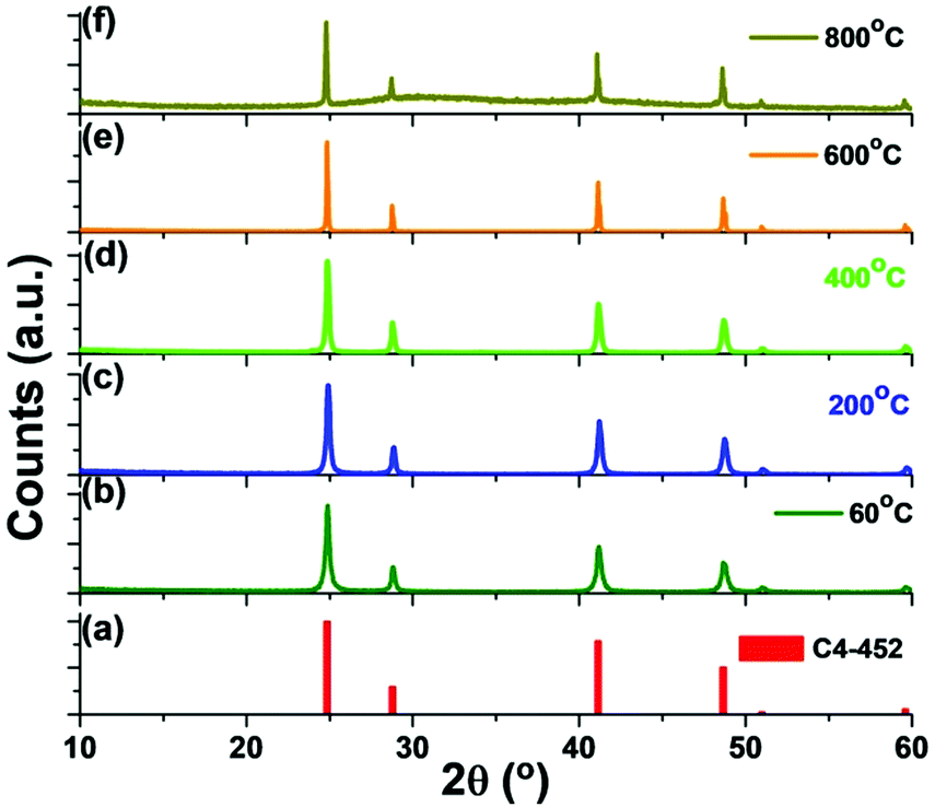 | ||
| Fig. 1 PXRD patterns of the as-prepared BaF2:Ce3+ (0.1%) nanoparticles and those calcined at different temperatures. | ||
The lattice strains of the as-prepared (P1) and calcined samples (P2–P5) have been determined using the Williamson–Hall equation (ESI†). The result indicates that tensile strain is occurring from the as-prepared nanoparticles (P1) to those calcined at 400 °C (P4). However, the maximum tensile strain is obtained for the as-prepared (at 60 °C, P1) sample (η = 0.95%). On the other hand, the samples calcined at higher temperatures reveal the development of compressive strain with strain values of −0.298% and −0.212% for the samples calcined at 600 °C (P4) and 800 °C (P5), respectively (Fig. 2 and Table 1).
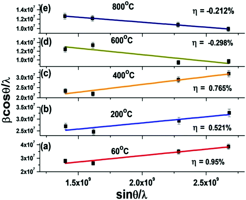 | ||
| Fig. 2 Lattice strain of BaF2:Ce3+ (0.1%) nanoparticles and those calcined at different temperatures. | ||
| Sample ID | Samples | Phase | Crystallite size (111) (nm) | Cell volume (Å3) | A (Å) | Average lattice strain (η%) |
|---|---|---|---|---|---|---|
| P1 | BaF2–Ce (0.1%) (as-prepared, 60 °C) | Cubic | 32.2 (±0.3) | 238.07(16) | 6.197(24) | 0.95 (tensile) |
| P2 | BaF2–Ce (0.1%) (calcined-200 °C) | Cubic | 36.2 (±0.3) | 238.13(5) | 6.198(7) | 0.546 (tensile) |
| P3 | BaF2–Ce (0.1%) (calcined-400 °C) | Cubic | 38.5 (±0.3) | 238.07(7) | 6.197(11) | 0.765 (tensile) |
| P4 | BaF2–Ce (0.1%) (calcined-600 °C) | Cubic | 71.3 (±0.3) | 238.45(15) | 6.201(22) | −0.298 (compressive) |
| P5 | BaF2–Ce (0.1%) (calcined-800 °C) | Cubic | 72.4 (±0.3) | 239.33(9) | 6.208(14) | −0.212 (compressive) |
3.2 Thermal properties
It is previously reported that on reducing the size of particles from the bulk to the nanoscale, the melting point is reduced and can be expressed as40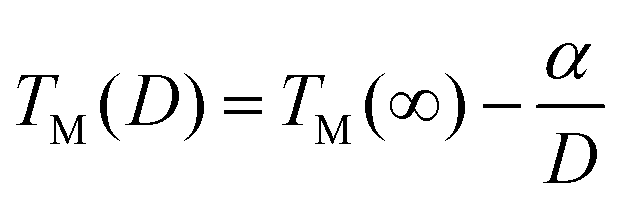 | (1) |
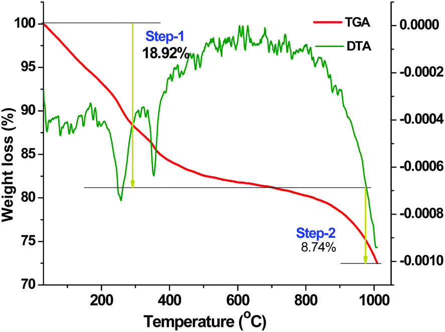 | ||
| Fig. 3 TGA and DTA curves of the as-prepared BaF2:Ce3+ (0.1%) nanoparticles synthesized using the [C4mim][BF4] ionic liquid. | ||
There is a well established relationship between the size of particles and the width of an endothermic peak, which suggests that the broadening of the endothermic peak is related to the particle size decreasing. Thus, it is likely that the size of the particles responsible for the peak at 248 °C is smaller than that responsible for the peak at 352 °C. Normally, the melting point of bulk BaF2 is 1386 °C.42 In our earlier report, we have noticed a broad endothermic peak at 400 °C for BaF2:Eu3+ nanoparticles and this endothermic event was ascribed to surface melting or full melting.42 So, in the present case it may be indicated that a melting-like situation arises at 248 °C and 352 °C.
3.3 Morphology and local structure
Fig. 4 depicts high magnification FESEM images of the as-prepared (P1) and calcined BaF2 nanoparticles (P2–P5). The as-synthesized nanoparticles appear as nanoflakes (Fig. 4a and b). However, at the beginning of calcination, the as-prepared nanoparticles tend to agglomerate, which leads to the formation of larger particles. The edges of the BaF2 nanoflakes get thicker and blunt till 400 °C (as shown in Fig. 4c). But a significant change in morphology appears when they are calcined at 600 °C (Fig. 4d and e and Fig. S1a, ESI†). At 600 °C, we observe the formation of larger size particles with big pores that result from merging of the nanoflakes with each other (Fig. 4d and e and Fig. S1a, ESI†). From thermal analysis it is conceived that surface melting or a melting-like situation arises around 354 °C. So nicely connected, bigger size nanoparticles obtained at 600 °C appear first due to melting of nanoparticles which are then re-assembled on cooling (Fig. 4d and e, inset and Fig. S1a, ESI†). This is further supported by zooming, which reveals the surface of bigger particles to be comprised of tiny particles (see Fig. 4e inset and Fig. S1a, ESI†). This kind of growth is normally associated with the terminology ‘secondary nucleation’.39,42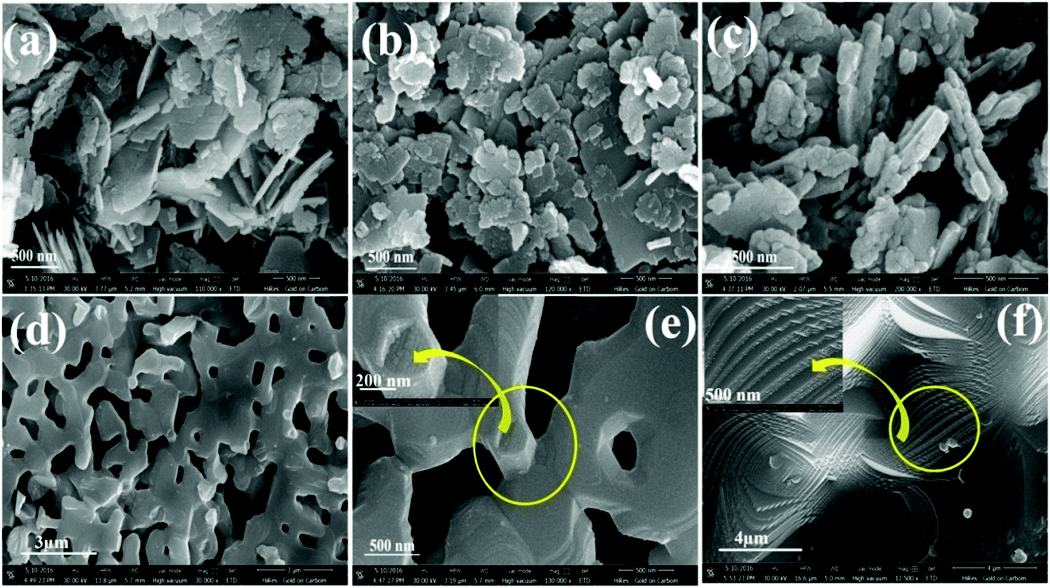 | ||
| Fig. 4 High magnification FESEM images of (a) as-prepared BaF2:Ce3+ (0.1%) dried at 60 °C, and samples calcined at different temperatures (b) 200 °C, (c) 400 °C, (d) 600 °C, (e) 600 °C, and (f) 800 °C. | ||
The above presented results suggest that calcining the as-prepared nanoparticles at high temperature initially results in surface melting that further leads to smoothing the surface and the formation of a layer-like structure. Again a step/stair-like morphology appears when the samples are calcined at 800 °C (Fig. 4f and Fig. S1b, ESI†). Here the pattern of the step/stair-like shape at 800 °C becomes more regular than that of the calcined sample at 600 °C (P4) while the pores on the surface completely vanish. The latter indicates that at high temperature (800 °C), small particles get further reassembled and subsequently gathered in a layer-by-layer manner while cooling to room temperature. In this way, formation of layer or step/stair-like structures takes place (Fig. 4f and Fig. S1b, ESI†). Fig. 5 and Fig. S2 (ESI†) illustrate the TEM and HRTEM images of the as-prepared (60 °C) (P1) and calcined nanoparticles at 400 °C (P3), 600 °C (P4) and 800 °C (P5) respectively. The TEM images demonstrate that the as-prepared nanoparticles are square/rectangular disc shaped and are highly agglomerated. The nanoparticles which have undergone calcining at a temperature of 400 °C demonstrate blunt and smoother edges of the square/rectangular discs compared to the as-prepared sample (Fig. 5c and d). Such kinds of changes have been already observed in the highly magnified FESEM images of the same sample (400 °C calcined sample, P3). Meanwhile, the morphology is shown to drastically transform from square/rectangular disc-shape to highly agglomerated irregular spherical shape on calcining at 600 °C. The irregular spherical shape particles reveal agglomeration, which gives rise to the formation of the bigger size particles. The 800 °C calcined sample is also comprised of some amount of small, non-uniform spherical shape particles which are highly agglomerated to form bigger size particles. These results evidently confirm the transformation of the morphology from square/rectangular shape nanoparticles to a layer-like structure depending on the calcination temperature, which can be clearly seen from the FESEM images (Fig. 4 and Fig. S1, ESI†). To depict the growth of the particles in the nanoscale regime, we have performed a comprehensive study of high-resolution TEM (HRTEM) images.
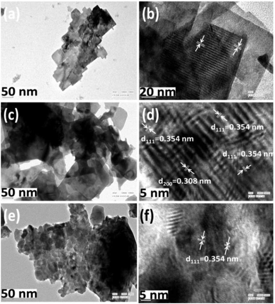 | ||
| Fig. 5 TEM and HRTEM images of BaF2:Ce3+ (0.1%) nanoparticles: (a and b) as-prepared (60 °C), (c and d) calcined at 400 °C and (e and f) calcined at 600 °C. | ||
It was revealed that the growth of the nanoparticles takes place along the predominant (111) plane. In addition to the (111) plane, the (200) plane also contributes to the growth of the particles calcined at 400 °C. Whilst the samples calcined at 600 °C (P4) and 800 °C (P5) predominately grow along the (111) plane, the 800 °C calcined sample (P5) demonstrates the presence of substantial point defects. We relate the latter to missing atoms from the array of the planes, which are marked by a rectangular box and circles in Fig. S2 (ESI†). The composition and distribution of ions in the as-prepared 0.1% Ce-doped BaF2 nanoparticles are confirmed through EDX and elemental mapping (Fig. S3 and S4, ESI†). A considerable change in surface area upon calcination is noticed.
To further confirm the presence of a calcination temperature-dependent change in the morphology of the samples, we have performed BET surface area analysis. The as-prepared sample shows a relatively high surface area (25.29 m2 g−1). Upon calcining the samples, the surface area demonstrates a well pronounced decrease. For example, for the 200 and 400 °C calcined samples the surface areas are found to be 14.45 m2 g−1 and 10.22 m2 g−1 respectively. However, a significant decrease in the specific surface area is noticed for the 600 °C (1.54 m2 g−1) sample, confirming coalescence of nanoparticles after a certain annealing temperature.
3.4 Luminescence properties
Fig. 6 shows the photoluminescence excitation and emission spectra of the as-prepared (P1) and calcined at different temperatures (P2⋯P5) BaF2:Ce3+ (0.1%) nanoparticles. The emission spectra of P1, P2 and P3 nanoparticles present an emission band centered near 352 nm. The band is best resolved in the case of the as-prepared nanoparticle (P1) sample with local peaks located at 330 and 355 nm, which correspond to electric-dipole transitions from the lowest 5d(2Eg) level to spin–orbit coupled 4f(2FJ) states.43 The excitation spectrum recorded monitoring the maximum of the emission band at 352 nm is dominated by a broad excitation band centered near 290 nm, which is assigned to the electronic transition from the ground state 4f(2F5/2) to the doublet 2E(eg) state (unresolved) of the excited 5d state.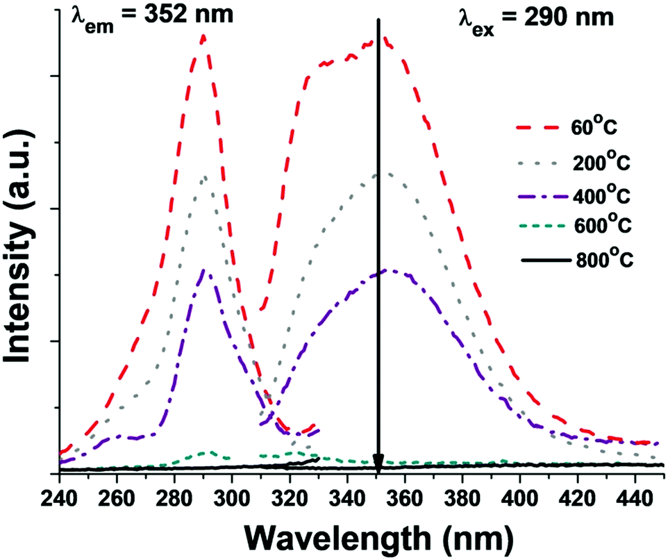 | ||
| Fig. 6 Photoluminescence excitation and emission spectra of the as-prepared (60 °C) and BaF2:Ce3+ (0.1%) nanoparticles calcined at different temperatures. | ||
As long as the samples are measured in nearly the same conditions, their spectra can be confronted and compared. Comparing the emission spectra of the samples shows that the highest intensity of the Ce3+ 5d–4f emission peak is observed for the as-prepared (60 °C calcined, P1) sample.
The emission peak intensity drops to less than half of its initial value for the 400 °C calcined sample (P3) and vanishes for the sample calcined at 600 °C and above (Fig. 6). Obviously, a similar process is observed for the excitation spectra (Fig. 6). These observations suggest that the Ce3+ emission is suppressed in the samples treated at high calcination temperature. Very recently, we have reported quenching of Eu3+ emission in BaF2:Eu3+ nanoparticles beyond calcination of 400 °C. A secondary nucleation mediated morphology change was noticed at higher temperature for BaF2:Eu3+ nanoparticles. From elemental mapping, surface area and other analyses, it was concluded that on calcining, Eu3+ ions are more likely to appear at the surface of the BaF2 nanoparticles rather than within the asymmetric lattice, which eventually leads to the concentration dependent quenching at higher calcination temperature.42 It is worth noting that segregation of rare-earth or transition metal ions on the surface of nanoparticles was also documented elsewhere.44–49 In the present case we also witness a drastic morphology change due to secondary nucleation that is pronounced at higher calcination temperatures. The surface area diminishes to a great extent at higher calcination temperatures (600 and 800 °C), which indicates that Ce3+ can appear more likely on the surface, which in turn is favorable for concentration quenching. Another reason for the quenching of Ce3+ emission in the samples with increased calcination temperature is connected with the oxygen atoms (originating from the IL or precursors), which can penetrate the anionic sublattice at high temperature. A similar effect was earlier documented for CaF2 nanoparticles.
3.5 Thermally stimulated luminescence and exoelectron emission
Intrinsic and impurity-related defects are well known to govern the optical and luminescence properties of single and polycrystalline materials, while for nanostructured materials they are expected to become of particular importance. This is connected with the extended grain boundaries and surfaces. Uncontrolled impurities and defects typically form electron and hole traps which can capture intrinsic electronic excitations and affect the dynamics and efficiency of host-to-impurity energy transfer, which is obviously unwanted for scintillator materials, including BaF2:Ce3+. To get insight into the nature of traps in optical and luminescence materials a TSL method is widely applied. The method allows determination of the energy level structure and concentration (content) of defects in a particular volume of material and further evaluates their influence on the optical and luminescence properties of the material. Turning to nanostructured materials requires paying greater attention to surface-related defects and therefore applying surface sensitive methods of experimental study such as TSEE. The latter allows the detection of electrons emitted from the sample surface. Thus, simultaneous measurements of TSL and TSEE signals allow identification and sorting of trapping centers into hole and electron ones. Such information is particularly useful when considering the kinetics of processes related to charge transfer from the traps to emission centers.Fig. 7 presents TSL and TSEE glow curves recorded for the as-prepared (60 °C) and the calcined samples at different temperatures. Obviously, the TSL and TSEE glow curves for all the samples are characterized by a complex structure resulting from a superposition of multiple peaks. The glow curves were fitted assuming first order kinetics of thermal processes.48,49 The TSEE and TSL activation energies were calculated using specialized software, which is based on widely accepted algorithms and methods.50,51 The quality of the fittings done in the frame of this research was satisfactory as long as the figure-of-merit (FOM) was normally less than 1%. The kinetics parameters obtained for the TSEE and TSL glow curves, which include the peak maxima (Tm), activation energies (Ea), and frequency factor (S), are gathered in Table 2. On analyzing the glow curves and kinetic parameters such as Ea and S, it is noticed that increasing the calcination temperature does not lead to linear variation of the Ea and S values. Nevertheless we may highlight the following most pronounced peculiarities of the TSEE and TSL processes in the nanoparticles of 0.1% Ce3+ doped BaF2: first, the as-prepared nanoparticles (P1) demonstrate the presence of relatively deep traps of electron character which appear mostly between 250 and 450 °C (Fig. 7).
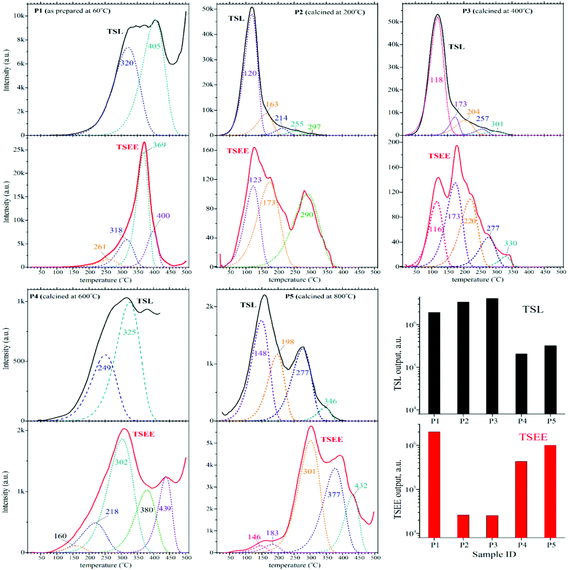 | ||
| Fig. 7 TSL and TSEE glow curves recorded for the as-prepared (60 °C) (P1) and calcined at 200 °C (P2), 400 °C (P3), 600 °C (P4) and 800 °C (P5) BaF2:Ce3+ (0.1%) nanoparticles exposed to equal doses of the electron beam. Peak maximum temperatures (Tm, K) are shown near each peak. The bar diagram demonstrates the integrated output of the TSL and TSEE signals as accumulated through the temperature range of the measurement for each sample. | ||
| Sample | Process | Kinetic parameter | Peaks | ||||
|---|---|---|---|---|---|---|---|
| 1 | 2 | 3 | 4 | 5 | |||
| The notations of the parameters obtained for the TSEE and TSL glow curves are Tm (peak maxima), Ea (activation energies) and S (frequency factor). | |||||||
| As prepared (60 °C) | TSL | T m | 405 | 320 | |||
| E a | 1.12 | 0.73 | |||||
| S | 2.17 × 10⁶ | 1.55 × 10⁴ | |||||
| TSEE | T m | 400 | 369 | 317 | 261 | ||
| E a | 2.34 | 1.97 | 1.21 | 0.82 | |||
| S | 7.94 × 10 15 | 6.50 × 10¹³ | 3.46 × 10⁸ | 6.57 × 10⁵ | |||
| Calcined at 200 °C | TSL | T m | 297 | 255 | 214 | 163 | 119 |
| E | 1.39 | 1.18 | 1.03 | 0.69 | 0.65 | ||
| S | 4.86 × 10¹⁰ | 4.61 × 10⁹ | 1.20 × 10⁹ | 1.97 × 10⁶ | 4.86 × 10⁶ | ||
| TSEE | T m | 290 | 173 | 123 | |||
| E a | 0.64 | 0.57 | 0.48 | ||||
| S | 6.43 × 10³ | 3.30 × 10³ | 3.35 × 10⁵ | ||||
| Calcined at 400 °C | TSL | T m | 301 | 257 | 204 | 173 | 118 |
| E | 1.05 | 1.25 | 0.72 | 1.19 | 0.65 | ||
| S | 3.19 × 10⁷ | 1.92 × 10¹⁰ | 6.56 × 10⁵ | 9.44 × 10¹¹ | 6.41 × 10⁶ | ||
| TSEE | T m | 330 | 277 | 220 | 173 | 116 | |
| E a | 1.72 | 1.01 | 0.76 | 0.67 | 0.59 | ||
| S | 6.74 × 10¹² | 3.62 × 10⁷ | 1.19 × 10⁶ | 8.01 × 10⁵ | 9.95 × 10⁵ | ||
| Calcined at 600 °C | TSL | T m | 325 | 249 | |||
| E a | 0.79 | 0.58 | |||||
| S | 3.76 × 10⁴ | 2.54 × 10³ | |||||
| TSEE | T m | 439 | 380 | 302 | 218 | 160 | |
| E a | 2.08 | 1.13 | 0.70 | 0.53 | 0.54 | ||
| S | 6.81 × 10¹² | 5.03 × 10⁶ | 9.52 × 10³ | 1.90 × 10³ | 2.03 × 10⁴ | ||
| Calcined at 800 °C | TSL | T m | 346 | 277 | 198 | 148 | |
| E a | 1.65 | 0.84 | 0.73 | 0.54 | |||
| S | 6.89 × 10¹¹ | 8.35 × 10⁵ | 1.12 × 10⁶ | 5.28 × 10⁴ | |||
| TSEE | T m | 432 | 377 | 301 | 183 | 146 | |
| E a | 1.92 | 1.10 | 0.84 | 0.72 | 0.70 | ||
| S | 1.23 × 10¹² | 5.25 × 10⁶ | 3.27 × 10⁵ | 1.86 × 10⁶ | 5.77 × 10⁶ | ||
Second, the TSL and TSEE glow curves recorded for the nanoparticles calcined at 200 °C (P2) and 400 °C (P3) drastically differ from those demonstrated for the as-prepared sample. This correlates well with the significant changes in the morphology related to the secondary nucleation that occurs in the calcined nanoparticles.
The structure of the defects in the 200 and 400 °C calcined samples is quite similar and is characterized by the presence of traps mostly appearing between 50 and 200 °C. The TSEE output in the corresponding temperature range is very low and is two orders lower than that observed for the as-prepared sample. This suggests that the traps appearing in the nanoparticles calcined at 200 and 400 °C mostly have a hole character (Fig. 7).
Third, the samples calcined at 200 and 400 °C demonstrate the lowest integrated output of TSEE and the highest integrated output of TSL. The TSL output is about 100 times higher than that for TSEE in these samples. This suggests that the detected thermal disintegration of trapping centers is mostly related to defects located within the particles’ ‘volume’, not to those related to the surface. This fact correlates with the above described smoothing and blunting of the nanoparticles, which appears as ‘healing’ of the particle surface, i.e. lowering the density of surface-related defects. Note that the most prominent TSL features are followed by the TSEE ones. This fact indicates that the disintegration of trapping centers (defects) is mostly accompanied by the migration of electrons to the glow centers via the conduction band. The latter obviously gives rise to electron emission from the nanoparticles. Note that such a phenomenon becomes less pronounced for the sample calcined at 600 °C (P4) and is not observed for the sample calcined at 800 °C (P5). Finally, turning to the calcination temperature of 600 °C gives rise to a significant (about 20 times) drop of the TSL output in comparison to that observed for the samples calcined at 200 and 400 °C. This is followed by a similar degree increase of the TSEE output. The TSL output further increases by a factor of 1.5 and the TSEE output increases by factor of 2 for the sample calcined at 800 °C. Another important tendency observed for the samples calcined at 600 and 800 °C is related to the domination of deeper electron traps, which appears as a high-temperature shift of the TSEE glow peaks. The most pronounced features in the TSEE and TSL glow curves recorded for the 800 °C calcined sample do not correlate with each other and demonstrate most noticeable distinctions. This phenomenon is connected with the formation of new types of defects that do not appear in the smaller nanoparticles synthesized at lower temperatures. Among those defects can be F vacancies (F-centers) that are typical for bulk BaF2 crystals.52 This correlates with the formation of larger nanoparticles in high-temperature synthesis (as shown above). Another consequence arising from the formation of larger nanoparticles is connected with the lowering of the surface to volume ratio. This should potentially reduce the interaction of excited Ce3+ ions with the surface-related defects. It is worth noting that the appearance of the TSL glow curve recorded for the nanoparticles calcined at 800 °C well correlates with that recently documented for an optimized BaF2:Ce3+ nanophosphor with an average particle size of 100 nm.53
Fig. 8 shows an energy level diagram for the data presented in Table 2. The diagram depicts the Ce3+ 4f ground state and the lowest energy 5d state located within the forbidden gap.54 The energy levels of the electron and hole traps are located through the above-described synchronic measurements of TSL and TSEE glow curves. The diagram demonstrates the fact that the most effective mechanism to transfer energy from host electronic excitations to Ce3+ ions at high temperatures is realized through the electron–hole recombination process.55
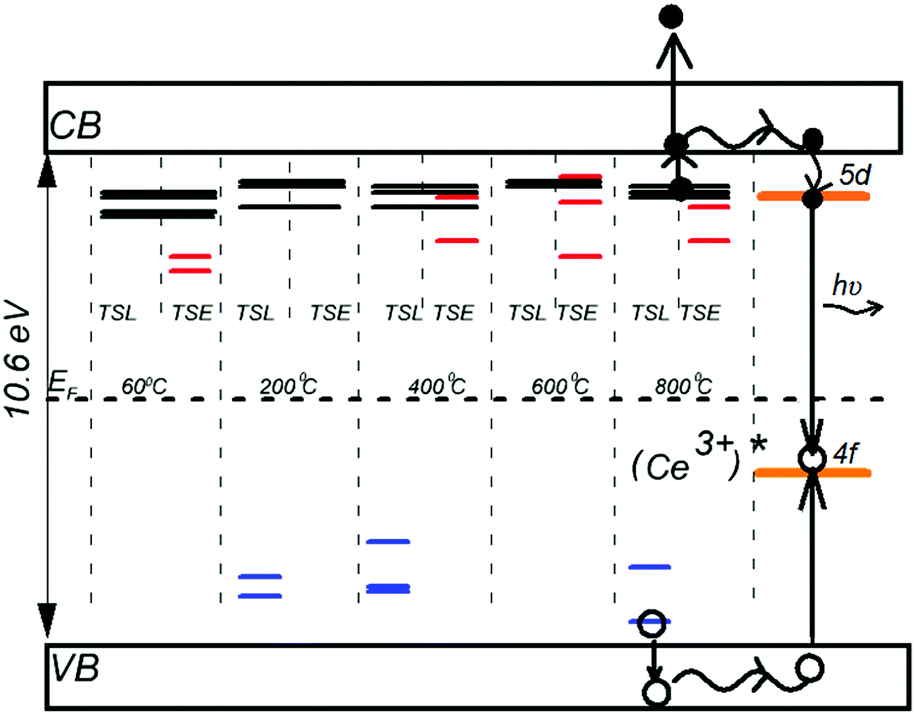 | ||
| Fig. 8 Energy level diagram demonstrating the location of electron and hole traps in BaF2:Ce3+ (0.1%) nanoparticles calcined at different temperatures. Black-marked energy levels correspond to the traps which are simultaneously detected through TSEE and TSL. Red- and blue-marked energy levels correspond to the traps detected only through TSEE or TSL, respectively. | ||
Thermal activation of electron and hole traps results in delocalization of the carriers to the conduction and valence bands. The delocalized carriers may further interact with cerium ions. Excitation of a Ce3+ ion generally starts with the capture of a hole from the VB and formation of a Ce4+ ion, which further attracts an electron from the CB to promote recombination. The dynamics of this process can be significantly affected by re-trapping of carriers on defects.
It is worth noting that the TSL and TSEE techniques have obvious limitations. First of all, there is some degree of uncertainty in the actual temperature of the sample. The temperature gradient between the lower and upper surface of the sample may vary depending on the crystal structure and density of the sample. Structural inhomogeneity may lead to the appearance of additional glow peaks. It is quite often that the TSL curves recorded for single crystals differ from those recorded for polycrystalline or powdered samples.56 Another phenomenon that may give rise to uncertainty in the interpretation of TSEE features arises from thermal decomposition of the organic precursor or ionic liquid remaining on the surface of the nanoparticles. To exclude the uncertainties mentioned above, additional studies with VUV and EPR spectroscopy are required to get insight into the molecular and energy structure of the defects observed.
4. Conclusion
In summary, we have successfully synthesized single phase BaF2 nanoparticles doped with 0.1% Ce3+ using a task specific ionic liquid ([C4mim][BF4]) where the IL works as a solvent, a templating agent and a fluoride source, i.e. all ‘three in one’. On calcining the samples from 60 to 800 °C, a significant effect on the lattice strain and morphology is observed. The lattice strain changes from tensile to compressive on increasing the calcination temperature. However, the morphology of the nanoparticles changes from a cubic/rectangular shape (as-prepared) to layer like structures (calcining the samples above 600 °C). This morphological change is fundamentally controlled by secondary nucleation of nanoparticles at high temperature (>600 °C). Another important effect of the calcination temperature is found on the PL intensity of the nanoparticles, in which the emission intensity is abruptly decreased with increasing the calcination temperature and vanishes for the sample calcined at 600 °C. Simultaneous measurements of TSL and TSEE glow curves allowed general identification of hole and electron trapping centers, which were found to significantly vary in the samples calcined at different temperatures. Analysis reveals that along with deeper electron traps that appear as a high-temperature shift of the TSEE glow peaks for both 600 and 800 °C, some new types of defects like F vacancies (F-centres) can be present and affect the luminescence at high calcination temperature. The samples prepared at high calcination temperature are also shown to experience quenching of luminescence related to segregation of Ce3+ dopant ions on the nanoparticles’ surface as a result of secondary nucleation mediated morphology changes at higher calcination temperature. All these phenomena cumulatively quench the Ce3+ luminescence in nanoparticles calcined at high temperature. Nevertheless, the presented results suggest the presence of an evidently strong correlation between the synthesis conditions and morphology, defect structure and luminescence characteristic of nanoparticles that can be further used for tailoring nanomaterials with controlled properties.Conflicts of interest
There are no conflicts to declare.Acknowledgements
The authors would like to acknowledge financial support from the Science and Engineering Research Board (SERB) [SERB No: SB/FT/CS-014/2014], and Board of Research in Nuclear Sciences (BRNS) [Sanction No. 34/14/27/2016-BRNS/34368], Government of India. P. G. acknowledges SERB for providing an International Travel Grant (ITS/2018/003736) to participate in a conference in Russia. The authors acknowledge the Sophisticated Instrumentation Centre (SIC) for SEM, Department of Chemistry for PXRD analysis and PURSE programme sanctioned by the Department of Science and Technology (DST), Govt of India. The authors also acknowledge AIIMS New Delhi for TEM characterization. A. I. S., K. V. I. and I. I. L. acknowledge partial support from the UrFU Competitiveness Enhancement Program.References
- X. Qin, X. Liu, W. Huang, M. Bettinelli and X. Liu, Chem. Rev., 2017, 117, 4488–4527 CrossRef CAS PubMed.
- S. Gai, C. Li, P. Yang and J. Lin, Chem. Rev., 2014, 114, 2343–2389 CrossRef CAS PubMed.
- S. V. Eliseeva and J.-C. G. Bünzli, Chem. Soc. Rev., 2010, 39, 189–227 RSC.
- R. K. Sharma, A.-V. Mudring and P. Ghosh, J. Lumin., 2017, 189, 44–63 CrossRef CAS.
- C. D. S. Brites, P. P. Lima, N. J. O. Silva, A. Millán, V. S. Amaral, F. Palacio and L. D. Carlos, New J. Chem., 2011, 35, 1177–1183 RSC.
- X.-C. Shao, S.-M. Zhou, Y.-R. Tang, X.-Z. Yi, D.-M. Hao and J. Chen, J. Inorg. Mater., 2018, 33, 1119–1123 CrossRef.
- M. Šimurda, M. Boča, P. Švec, P. Švec Jr., D. Janičkovič, Z. N. Shiand and J. Mlynáriková, New J. Chem., 2018, 42, 4612–4623 RSC.
- N. P. Singh, N. Kumam, L. P. Singh, N. R. Singh and K. Srivastava, New J. Chem., 2019, 43, 1328–1339 RSC.
- D. Valiev, T. Han, S. Stepanov, V. Vaganov and V. Paygin, Mater. Res. Express, 2018, 5, 096201 CrossRef.
- T. Kato, G. Okada, K. Fukuda and T. Yanagida, Radiat. Meas., 2017, 106, 140–145 CrossRef CAS.
- M. Siebold, S. Bock, U. Schramm, B. Xu, J. L. Doualan, P. Camy and R. Moncorgé, Appl. Phys. B: Lasers Opt., 2009, 97, 327–338 CrossRef CAS.
- V. V. Vistovskyy, A. V. Zhyshkovych, O. O. Halyatkin, N. E. Mitina, A. S. Zaichenko, P. A. Rodnyi, A. N. Vasil’ev, A. V. Gektin and A. S. Voloshinovskii, J. Appl. Phys., 2014, 116, 054308 CrossRef.
- E. A. McKigney, R. E. Del Sesto, L. G. Jacobsohn, P. A. Santi, R. E. Muenchausen, K. C. Ott, T. M. McCleskey, B. L. Bennett, J. F. Smith and D. W. Cooke, Nucl. Instrum. Methods Phys. Res., Sect. B, 2007, 579, 15–18 CrossRef CAS.
- R. K. Feller, G. M. Purdy, D. Ortiz-Acosta, S. Stange, A. Li, E. A. McKigney, E. I. Esch, R. E. Muenchausen, R. Gilbertson, M. Bacrania, B. L. Bennett, K. C. Ott, L. Brown, C. S. Macomber, B. L. Scott and R. E. Del Sesto, J. Mater. Chem., 2011, 21, 5716–5722 RSC.
- L. G. Jacobsohn, K. B. Sprinkle, C. J. Kucera, T. L. James, S. A. Roberts, H. Qian, E. G. Yukihara, T. A. DeVol and J. Ballato, Opt. Mater., 2010, 33, 136–140 CrossRef CAS.
- X. Duan, J. Ma, J. Lianc and W. Zheng, CrystEngComm, 2014, 16, 2550–2559 RSC.
- P. Ghosh, R. K. Sharma, Y. N. Chouryal and A.-V. Mudring, RSC Adv., 2017, 7, 33467–33476 RSC.
- R. K. Sharma, Y. N. Chouryal, S. Chaudhari, J. Saravanakumar, S. R. Dey and P. Ghosh, ACS Appl. Mater. Interfaces, 2017, 9, 11651–11661 CrossRef CAS PubMed.
- S. Anghel, S. Golbert, A. Meijerink and A.-V. Mudring, J. Lumin., 2017, 189, 2–8 CrossRef CAS.
- J. Cybińska, C. Lorbeer and A.-V. Mudring, J. Mater. Chem., 2012, 22, 9505–9508 RSC.
- C. Lorbeer, F. Behrends, J. Cybinska, H. Eckert and A.-V. Mudring, J. Mater. Chem. C, 2014, 2, 9439–9450 RSC.
- R. D. Rogers and K. R. Seddon, Science, 2003, 302, 792–793 CrossRef.
- M. Armand, F. Endres, D. R. Macfarlane, H. Ohno and B. Scrosati, Nat. Mater., 2009, 8, 621–629 CrossRef CAS.
- J. P. Hallett and T. Welton, Chem. Rev., 2011, 111, 3508–3576 CrossRef CAS.
- S. Zhang, J. Sun, X. Zhang, J. Xin, Q. Miao and J. Wang, Chem. Soc. Rev., 2014, 43, 7838–7869 RSC.
- P. Ghosh and A.-V. Mudring, Nanoscale, 2016, 8, 8160–8169 RSC.
- A. Meijerink, W. J. Schipper and G. Blasse, J. Phys. D: Appl. Phys., 1991, 24, 997–1002 CrossRef CAS.
- P. L. Antonio and L. V. E. Caldas, Radiat. Meas., 2017, 106, 538–542 CrossRef CAS.
- N. Kunkel, A. D. Sontakke, S. Kohaut, B. Vianaand and P. Dorenbos, J. Phys. Chem. C, 2016, 120, 29414–29422 CrossRef CAS.
- M. Buryi, P. Bohacek, K. Chernenko, A. Krasnikov, V. V. Laguta, E. Mihokova, M. Nikl and S. Zazubovich, Phys. Status Solidi B, 2016, 253, 895–910 CrossRef CAS.
- V. Y. Degoda, Y. P. Kogut, I. M. Moroz and F. A. Danevich, J. Lumin., 2017, 183, 424–432 CrossRef CAS.
- D. O. Junot, M. A. C. dos Santos, P. L. Antonio, L. V. E. Caldas and D. N. Souza, Radiat. Meas., 2014, 71, 99–103 CrossRef CAS.
- M. E. Haghiri, E. Saion, N. Soltani, W. S. wan Abdullah, M. Navasery, K. R. E. Saraee and N. Deyhimi, J. Alloys Compd., 2014, 582, 392–397 CrossRef.
- O. T. Antonyak, V. V. Vistovskyy, A. V. Zhyshkovych and I. M. Kravchuk, J. Lumin., 2015, 167, 249–253 CrossRef CAS.
- R. Hemam, L. R. Singh, S. D. Singh and R. N. Sharan, J. Lumin., 2018, 197, 399–405 CrossRef CAS.
- M. Kumar and S. K. Gupta, J. Lumin., 2015, 168, 151–157 CrossRef CAS.
- B. Zhou, L. Tao, Y. H. Tsang and W. Jin, J. Mater. Chem. C, 2013, 1, 4313–4318 RSC.
- F. Vetrone, R. Naccache, V. Mahalingam, C. G. Morgan and J. A. Capobianco, Adv. Funct. Mater., 2009, 19, 2924–2929 CrossRef CAS.
- A. S. S. Shafiqah, Y. M. Amin, R. M. Nor and D. A. Bradley, Radiat. Phys. Chem., 2015, 117, 102–107 CrossRef.
- K. F. Peters, Y.-W. Chung and J. B. Cohen, Appl. Phys. Lett., 1997, 71, 2391–2393 CrossRef CAS.
- K. Dick, T. Dhanasekaran, Z. Zhang and D. Meisel, J. Am. Chem. Soc., 2002, 124, 2312–2317 CrossRef CAS PubMed.
- R. K. Sharma, S. Nigam, Y. N. Chouryal, S. Nema, S. P. Bera, Y. Bhargava and P. Ghosh, ACS Appl. Nano Mater., 2019, 2, 927–936 CrossRef CAS.
- R. Visser, P. Dorenbos, C. W. E. van Eijk, A. Meijerink, G. Blassé and H. W. den Hartog, J. Phys.: Condens. Matter, 1993, 5, 1659–1680 CrossRef CAS.
- J. Bang, H. Yang and P. H. Holloway, Nanotechnology, 2006, 17, 973 CrossRef CAS.
- S.-J. Shih, Y.-Y. Wu and K. B. Borisenko, J. Nanopart. Res., 2011, 13, 7021–7028 CrossRef CAS.
- X. Weng, B. Perston, X. Z. Wang, I. Abrahams, T. Lin, S. Yang, J. R. G. Evans, D. J. Morgan, A. F. Carley, M. Bowker, J. C. Knowles, I. Rehman and J. A. Darr, Appl. Catal., B, 2009, 90, 405–415 CrossRef CAS.
- N. Salah, N. D. Alharbi, S. S. Habib and S. P. Lochab, J. Nanomater., 2015, 2015, 1–7, DOI:10.1155/2015/136402.
- R. Chen, J. Appl. Phys., 1969, 40, 570–585 CrossRef CAS.
- A. J. J. Bos, Radiat. Meas., 2007, 41, S45–S56 CrossRef CAS.
- A. I. Slesarev, Bull. Ural State Tech. Univ., 2006, 5, 174–179 Search PubMed.
- K. S. Chung, H. S. Choe, J. I. Lee, J. L. Kim and S. Y. Chang, Radiat. Prot. Dosim., 2005, 115, 345–349 CrossRef PubMed.
- A. J. Wojtowicz, P. Szupryczynski, J. Glodo, W. Drozdowski and D. Wisniewski, J. Phys.: Condens. Matter, 2000, 12, 4097–4124 CrossRef CAS.
- K. H. Gavhane, M. S. Bhadane, A. P. Jadhav, B. J. Patil, V. N. Bhoraskar, S. S. Dahiwale and S. D. Dhole, J. Lumin., 2019, 209, 316–320 CrossRef CAS.
- P. A. Rodnyi, I. V. Khodyuk and G. B. Stryganyuk, Phys. Solid State, 2008, 50, 1639–1643 CrossRef CAS.
- E. A. Radzhabov and A. I. Nepomnyashchikh, Russ. Phys. J., 2000, 43, 205–210 CrossRef CAS.
- T. Yanagid, Y. Fujimoto, Y. Yokot, K. Kamad, S. Yanagid, A. Yoshikaw, H. Yagi and T. Yanagitani, Radiat. Meas., 2011, 46, 1503–1505 CrossRef.
Footnote |
| † Electronic supplementary information (ESI) available. See DOI: 10.1039/c9nj04526k |
| This journal is © The Royal Society of Chemistry and the Centre National de la Recherche Scientifique 2020 |