
 Open Access Article
 This Open Access Article is licensed under a
 Creative Commons Attribution 3.0 Unported Licence
Bandgap determination from individual orthorhombic thin cesium lead bromide nanosheets by electron energy-loss spectroscopy†
Rosaria
Brescia
 a,
Stefano
Toso
bc,
Quentin
Ramasse
*de,
Liberato
Manna
b,
Javad
Shamsi‡
b,
Clive
Downing
f,
Arrigo
Calzolari
g and
Giovanni
Bertoni
*gh
a,
Stefano
Toso
bc,
Quentin
Ramasse
*de,
Liberato
Manna
b,
Javad
Shamsi‡
b,
Clive
Downing
f,
Arrigo
Calzolari
g and
Giovanni
Bertoni
*gh
aElectron Microscopy Facility, Istituto Italiano di Tecnologia, Via Morego 30, 16163 Genova, Italy
bNanochemistry Department, Istituto Italiano di Tecnologia, Via Morego 30, 16163 Genova, Italy
cInternational Doctoral Program in Science, Università Cattolica del Sacro Cuore, 25121 Brescia, Italy
dSuperSTEM, SciTech Daresbury Science and Innovation Campus, Keckwick Lane, Daresbury WA4 4AD, UK. E-mail: qmramasse@superstem.org
eSchool of Chemical and Process Engineering & School of Physics, University of Leeds, Leeds LS29JT, UK
fThe Advanced Microscopy Laboratory, CRANN, Trinity College Dublin (TCD), Dublin, Ireland
gCNR – Istituto Nanoscienze, Via Campi 213/A, 41125 Modena, Italy. E-mail: giovanni.bertoni@cnr.it
hIMEM – CNR, Istituto dei Materiali per l’Elettronica e il Magnetismo, Parco Area delle Scienze 37/A, 43124 Parma, Italy
First published on 20th October 2020
Abstract
Inorganic lead halide perovskites are promising candidates for optoelectronic applications, due to their high photoluminescence quantum yield and narrow emission line widths. Particularly attractive is the possibility to vary the bandgap as a function of the halide composition and the size or shape of the crystals at the nanoscale. Here we present an aberration-corrected scanning transmission electron microscopy (STEM) and monochromated electron energy-loss spectroscopy (EELS) study of extended nanosheets of CsPbBr3. We demonstrate their orthorhombic crystal structure and their lateral termination with Cs–Br planes. The bandgaps are measured from individual nanosheets, avoiding the effect of the size distribution which is present in standard optical spectroscopy techniques. We find an increase of the bandgap starting at thicknesses below 10 nm, confirming the less marked effect of 1D confinement in nanosheets compared to the 3D confinement observed in quantum dots, as predicted by density functional theory calculations and optical spectroscopy data from ensemble measurements.
New conceptsLead halide perovskites have attracted interest for their absorption and emission wavelength tunability, obtained by controlling their crystal size and shape. Among them, inorganic CsPbBr3 perovskites, obtained as 2D nanosheets, with micron-scale width, and thickness down to 4 nm, are prototype structures of uni-axial electronic confinement. To overcome the intrinsic limitation due to thickness distribution from the synthesis, and precisely measure the bandgap as a function of thickness, we use aberration-corrected scanning transmission electron microscopy (STEM) imaging together with high-resolution monochromated electron energy-loss spectroscopy (EELS) on individual crystals. We confirm that the nanosheets have an orthorhombic structure with rotated PbBr6 octahedra, and preferential (110) edge terminations on Cs atoms rather than Pb, as seen by direct imaging at 80 pm spatial resolution. We verify an increase of the bandgap starting at a thickness below 10 nm from EELS, in good agreement with the simulations from density functional theory. The gap opening in these structures with quantum confinement along the z-direction is lower than in CsPbBr3 quantum dots with 3D confinement. The combination of STEM and EELS provides the unique advantage to measure these size-dependent properties without ensemble averaging as is usually obtained from standard optical techniques. |
Introduction
The interest in lead halide perovskites (LHPs) was boosted recently after the demonstration of high efficiency of this class of materials in thin film photovoltaic devices, where the LHPs act as absorbing layers, with the power conversion efficiency of LHP-based solar cells having risen to over 25% in the last years.1 Among them, inorganic LHPs with CsPbX3 (X = Cl, Br, and I) compositions have attracted particular attention.2–4 Further support for this research direction has come from the possibility to synthesize CsPbX3 LHPs by colloidal routes,5,6 and the ability to fabricate nanocrystals with controlled sizes and geometries, such as nanocubes, nanoplatelets and ultrathin nanosheets.7,8 The structure and optical properties of these nanostructures have been studied in detail for nanocubes and nanoplatelets,9–11 but only recently has the bandgap from single nanocrystals with cubic shape been measured by high resolution electron energy-loss spectroscopy (EELS) in a scanning transmission electron microscope (STEM).12 This approach was originally used by Erni and Browning on CdSe quantum dots.13The structure of CsPbBr3 is commonly described as orthorhombic in bulk form (Pnma or Pbnm depending on the orientation of the crystallographic axes), while it can also be cubic (Pm![[3 with combining macron]](https://www.rsc.org/images/entities/char_0033_0304.gif) m) in the case of nanocrystals.6,14 Bulk CsPbBr3 has been recently studied at very high resolution by combining convergent beam electron diffraction and ptychography in an aberration-corrected STEM, pointing to a tetragonal (I4/mcm) symmetry, with out-of-phase rotated octahedra along the [001] direction at room temperature (RT).15 On the other hand, the orthorhombic structure (according to the Pbnm description)16 was confirmed in the case of small nanoplatelets by X-ray total scattering experiments.17 Platelets as thin as monolayers have been recently identified from optical data analysis, as a product of high-throughput robotic synthesis inside a mixture of other species.18
m) in the case of nanocrystals.6,14 Bulk CsPbBr3 has been recently studied at very high resolution by combining convergent beam electron diffraction and ptychography in an aberration-corrected STEM, pointing to a tetragonal (I4/mcm) symmetry, with out-of-phase rotated octahedra along the [001] direction at room temperature (RT).15 On the other hand, the orthorhombic structure (according to the Pbnm description)16 was confirmed in the case of small nanoplatelets by X-ray total scattering experiments.17 Platelets as thin as monolayers have been recently identified from optical data analysis, as a product of high-throughput robotic synthesis inside a mixture of other species.18
In summary, different possible phases were reported for nanostructures of CsPbBr3 with reduced dimensions. In this communication we address the structure of CsPbBr3 in the form of thin nanosheets (NSs, with thickness t down to ∼4 nm). This was carried out by statistical analysis, including model-based fitting, of the intensity of atomic resolution images obtained on a high-stability probe-corrected dedicated STEM instrument (Nion UltraSTEM, with typical spatial resolution ∼80 pm and sample drift <0.1 Å min−1 in the conditions used). Moreover, these extended thin nanocrystals are ideal candidates to study the effect of dimensionality on the electronic confinement in this system, the carriers being here strictly confined in the z-direction compared to 3D confined quantum dots (QDs). The bandgap widening with decreasing thickness is directly measured from individual nanosheets via high energy resolution monochromated electron energy-loss spectroscopy (EELS). The combination of STEM and EELS provides the unique advantage of measuring these size-dependent properties without ensemble averaging as would be obtained usually from standard optical techniques.
Experimental and theoretical methods
Synthesis of CsPbBr3 nanosheets
The CsPbBr3 nanosheets were prepared by an adaptation of the method first reported by us.19 First, a PbBr2 stock solution was prepared by dissolving 0.13 g of PbBr2, 2.5 ml of oleic acid (OA) and 2.5 ml of oleylamine (OLAM) in 25 ml of octadecene (ODE). The mixture was heated to 120 °C under vacuum and continuous stirring until the solid was completely dissolved. Upon cooling to room temperature, it remained limpid and stable for months. Second, a Cs–oleate stock solution in OA was prepared by dissolving 0.032 g of Cs2CO3 in 10 ml of OA, following the same procedure as the other solution. Finally, 3 ml of the PbBr2 stock solution were put in a 20 ml glass vial, and a further 12 ml of ODE were added, to reach a total volume of 15 ml. The vial was closed with a rubber-septum cap and heated to 150 °C. Once the temperature was stabilized, 585 μl of octanoic acid (OCTAC) and 265 μl of octylamine (OCTAM) were introduced by piercing the septum with a needle and subsequently injecting the chemicals through it with the help of a micropipette. The temperature was left to equilibrate again to 150 °C, and the stirring speed was set to 400 rpm. Then, 1 ml of the Cs–oleate solution was swiftly injected, and the temperature was kept constant at 150 ± 2 °C for 5 min. After this time, the solution was quenched by dipping the vial in a room-temperature water bath.Transmission electron microscopy and spectroscopy
For the transmission electron microscopy (TEM) analyses, one aliquot of the crude reaction mixture was diluted in an identical volume of hexane, and one single drop of the so-prepared solution was drop-cast on a holey-carbon-film-coated Cu TEM grid. Prior to sample deposition, the commercial carbon support grid was cleaned by baking in vacuum (<1 × 10⁻⁴ Pa) at 200 °C for 7 h. To remove the remaining excess of organics, the grid was washed by laying it on a paper tissue and drop casting 5–10 drops of pure hexane, paying attention that each drop was completely dried before casting the following one. After drop-casting of the NS suspension, an additional gentle outgassing bake in similar vacuum conditions for 8 hours (at 55 °C) was applied to the TEM grid, to minimize the risks of adventitious carbon contamination during the experiments. The presented data were collected only on nanosheets overhanging the holes of the carbon support films, to avoid the absorption contribution from the carbon supporting film on the image contrast and on the EEL spectra. Atomic resolution images of the nanosheets were acquired at 200 kV acceleration voltage in annular dark field (ADF) STEM imaging mode on a Nion UltraSTEM200 microscope, equipped with a probe aberration corrector (TCD, Dublin, Ireland). The convergence semi-angle was 27 mrad and the inner cutoff angle of the ADF detector was 99 mrad. The choice of 200 kV for imaging the thicker nanosheets was made to ensure high signal-to-noise imaging, while reducing ionization, the likely dominant damage mechanism in this material system, thanks to the high voltage.20 Please see Fig. S1 in the ESI† for further details. Statistical image intensity quantification was carried out using the well-documented model-based fitting approach as implemented in StatSTEM21 from an image area containing approximately 300 projected unit cells. Image simulations were obtained using the multi-slice code Dr Probe.22 Finite source size effects were approximated by convoluting the simulated images with a Gaussian profile of 80 pm full-width at half-maximum (FWHM).23 The comparison between the simulated images and the experiment was done by using Voronoi cells integration around the atomic columns to extract the integrated intensity (or ADF cross-sections),24 as implemented in Atomap.25 The atomic structures in the figures were plotted using the software VESTA.26 Atoms are represented by balls with a radius proportional to their atomic number Z. EEL spectra, in the form of 3D (x, y, E) datasets, were acquired at 60 kV on a Nion UltraSTEM100MC ‘Hermes’ aberration-corrected STEM, equipped with a Gatan Enfinium-ERS EEL spectrometer optimized with high stability power supplies (SuperSTEM, Daresbury, UK). This instrument is equipped with a Nion high-resolution ground-potential monochromator, with the optical setting and monochromator slit width used in these experiments adjusted to produce a full-width at half-maximum (FWHM) of the elastic peak (zero-loss, ZL, peak, as measured in vacuum away from the sample) <20 meV. The convergence semi-angle was 33 mrad and the collection semi-angle of the spectrometer was 44 mrad. The acquisition at 60 kV acceleration voltage ensures a better energy resolution and reduces the impact of retardation effects on the energy-loss spectrum, which may otherwise complicate the determination of the bandgap.27,28 However, at low kV, possible beam-induced damage from ionization (or radiolysis) is expected to be more pronounced.29 This was evidenced in our experiments by a faster onset of visible structural damage when imaging at 60 kV (see Fig. S2, ESI†), and this structural damage can be accompanied by a loss of features in the EEL spectrum. The latter can possibly precede any visible structural modifications: careful scrutiny of the EELS fine structure was thus used as the main criterion for possible beam-induced damage in the gap determination experiments. We were particularly careful in spreading the electron dose for the EELS experiments to ensure that the gap determination is as reliable as possible. The beam current was set to <5 pA, and the spectra were collected by summing up individual datapoints from spectrum images acquired over a large sample area, rather than acquiring a single long-exposure spectrum. This resulted in spectra with a high signal-to-noise ratio sufficient for accurate band gap determination, while minimizing the risks of damage to the sample thanks to the lower electron dose (beam current per unit area and per unit time). The ‘dual-EELS’ acquisition mode was used to mitigate the effects of the limited dynamic range of the CCD-based camera of the spectrometer. Two quasi-simultaneous spectra were recorded, one spectrum (low-loss) contains the ZL peak acquired at a short exposure time (10 ms), while the other spectrum (high-loss) contains the region of the bandgap acquired at a longer exposure time (100 ms). The total acquisition time for the two spectra at one pixel was about 110 ms. The low-loss spectrum is used to carefully align the spectra at the sub-pixel level in the energy dimension by fitting a Gaussian peak under the ZL peak. The result is applied to the corresponding high-loss spectrum. We assume no drift in energy during the fast drift tube change of the spectrometer from the low-loss to the high-loss region in the acquisition of a single pixel of the dataset. The dispersion of the spectrometer was fixed to 2 meV or 5 meV per channel, depending on the required energy range. No background subtraction from the spectra was performed to avoid extrapolation errors. The Kramers–Kronig analysis and the optical absorption spectrum were obtained from the experimental EELS data using the iterative procedure described by Egerton,30 which is a built-in routine in Digital Micrograph (Gatan, Inc.).Energy dispersive X-ray spectra (EDXS) were acquired with a windowless Bruker 6T|100 solid state detector with a 100 mm2 effective area, installed on the probe-corrected Nion UltraSTEM200 microscope (TCD, Dublin, Ireland), and were used to verify the atomic fraction of Cs, Pb and Br. The spectra from single nanosheets were quantified with the Cliff–Lorimer method, using the Kα peak of Br and the Lα peaks of Pb and Cs. The provided quantitative values result from the average spectrum obtained from a large area of the [001]-oriented NS used for ADF-STEM imaging, and a conservative relative error of 5% was considered to take into account possible channeling effects.
Density functional calculations
First principles calculations, based on density functional theory (DFT), were performed using the Quantum Espresso package. Thin CsPbBr3 films of different thicknesses were considered (N = 1, 2, 4, 6, 8, and 16 pseudo-cubic units). Each film was simulated through periodically repeated slabs with (1 × 1) lateral periodicity in the (x, y) plane (see Fig. S3, ESI†). Slabs were terminated by Cs–Br atoms and separated by ∼1 nm of vacuum in the direction perpendicular to the film (z), in order to avoid spurious interactions among replicas. A bulk structure (i.e. with full periodicity in the three x, y, z spatial directions) was also simulated for reference. The lateral edges of the NS were not considered, due to the very large lateral extension of the NS and the fact that the ADF-STEM images for structure determination and the EELS spectra were acquired well inside the NS and away from the edges. All the structures were relaxed self-consistently until the forces on each atom were smaller than 0.03 eV Å−1. We used the Perdew–Burke–Ernzerhof (PBE)31 approximation to the exchange correlation functional for the calculation of total energy and band structure. Non-bonding interactions, such as van der Waals terms, were accounted for by the semiempirical method proposed by Grimme.32 The hybrid PBE0 functional was used to correct the DFT deficiencies in reproducing the bandgap, without further atomic relaxation on the optimized PBE structures. Bandgaps were evaluated from the difference between the top of the valence band and the bottom of the conduction band. The bandgap values reported for the nanosheets were shifted by the difference between the calculated DFT bulk value and the experimental bandgap found at large thickness. Atomic potentials were described by ultrasoft pseudopotentials as available in the SSSP library.33 Semi-core 5s5p and 5d electrons were explicitly included as valence electrons for Cs and Pb atoms, respectively. Single particle wavefunctions (charge) were expanded in planewaves up to a kinetic energy cutoff of 60 Ry (600 Ry). To test the effect of vacancies, neutral cation (VPb0, VCs0) and anion vacancy (VBr0) point defects were simulated by placing a single vacancy (i.e. by removing a single atom) in a (2 × 2 × 2) bulk superstructure. The Brillouin zone was sampled with a (6 × 6) k-point grid in the case of 2D films, and with a (3 × 3 × 2) k-grid in the case of defective 3D structures.Results and discussion
STEM imaging
The typical outcome of these synthesis processes consists of a distribution of thin rectangular nanosheets, a few hundreds of nm to a few μm in lateral size, as can be seen in Fig. S4 in the ESI.† A high-resolution ADF-STEM image from a CsPbBr3 NS is presented in Fig. 1. The columns formed only by Cs (Z = 55) atoms and only by Br (Z = 35) atoms, as well as the mixed Br and Pb (Z = 82) columns, are easily recognizable if the image is qualitatively compared with [001] projections of the cubic (ICSD #97852) and orthorhombic CsPbBr3 (ICSD #97851) structures, respectively (see Fig. S5 in ESI†). A close inspection of the position of the Br columns reveals that the experimental image fits more accurately the [001] projection of the orthorhombic phase, characterized by a rotation of the Br octahedra in the (a, b) plane followed by a small tilt along the c direction (Fig. 1b). We used the Pbmn subset (space group no. 62) for the choice of the crystal axes (a = 8.36 Å and b = 8.52 Å) as derived from the experiment, while a value of c = 11.89 Å (as derived from DFT relaxation) was considered in the image simulations. This result is in agreement with the structure previously reported for the case of nanoplatelets (NPs).16 A direct measurement of the lattice parameter c is not directly possible from ADF-STEM due to the extremely large aspect ratio of the nanosheets. Fig. 1c shows a (2 × 2) cell detail from the experimental image without any filtering (raw). Only a skew correction was applied to compensate for the small distortion of the STEM scan (due to a minor systematic non-orthogonality of the scan directions). Fig. 1d shows the same (2 × 2) cells after averaging using a template matching procedure that identified 100 sub-regions of the experimental image having the same size as the (2 × 2) cell template. The average image exhibits a clear reduction of the noise with negligible loss in resolution. The orthorhombic cell contains two pseudo-cubic lattice units along the c-axis, comprising two PbBr6 octahedra, each one with a thickness of ∼0.6 nm. Although describing the structure as orthorhombic, we report in what follows the number N of pseudo-cubic units so that the comparison with the thickness values from the literature (often derived from cubic structures) is straightforward. In order to derive quantitative information from the ADF-STEM images (thickness, atomic termination), we performed a statistical intensity analysis, using the model-based fitting approach implemented in StatSTEM.21 This methodology, first applied in ADF-STEM imaging to a SrTiO3 perovskite,34 a structure similar to the present one, was proven to give high accuracy in atom counting down to single atom precision.35 We limited our analysis to the Pb–Br1 columns and Cs columns, neglecting the Br2 columns for simplicity. Unfortunately, we cannot separate the Br1 atoms of the octahedra in Wyckoff position 4c from the Pb atoms in [001] projection. These Br atoms account for 1/3 of the total amount of Br, the other two thirds being the Br2 atoms (site 8d) forming the square projection of the octahedron when seen in [001] projection. Moreover, Pb atoms, being heavier, will contribute to the majority of the ADF intensity arising from the column. The results of the statistical-based fitting are presented in Fig. 1e for 650 atomic columns across the experimental image. Clearly, Cs columns give on average higher counts (12.7) than Pb–Br1 columns (9.8). Rounding the numbers, we can estimate the NS consists of 13(1) Cs planes and 10(1) Pb planes. This means a Pb/Cs ratio of 0.77(6). This result is in good agreement with the EDXS quantification obtained from integrating the signal over a large area from the very same NS (Pb/Cs = 0.79(4)). Assuming Cs-terminated surfaces (the validity of this assumption is discussed below) along the c-axis of a NS with thickness N = 13 (corresponding to ∼7.2 nm, not considering the ligands), the stoichiometric structure should yield a ratio Pb/Cs = 0.92. Our image intensity analysis therefore suggests a partial occupancy of Pb f = 0.85(7) for the bulk composition of the NS. A simulated STEM image calculated using these parameters (N = 13, Cs termination, f = 0.85) is presented in Fig. 1f. The atomic positions are well reproduced by the model. Fig. 1g shows the integrated intensity obtained using Voronoi cells integration of the atomic columns from [001] projections. The experiment (from Fig. 1d) is compared with a simulation from NS (N = 13) with only Pb vacancies (Pb occupancy f = 0.85, red bars) and the same NS by considering additional Br vacancies to maintain charge neutrality and balance the Pb vacancies (Br2 occupancy also f = 0.85, orange bars). The latter gives the best match for all column types, and results in an inner NS stoichiometry of CsPb0.85Br2.7 (that is, not considering the termination). This result is also supported by EDXS quantification, indicating a Br/Cs ratio of 2.3(1). The result from a CsPbBr3 bulk crystal is also shown in Fig. 1g for reference (purple bars). In the simulations, all the Debye–Waller (DW) factors for the different atoms were kept at the values found in literature from X-ray diffraction.36 Further minor adjustments in the integrated intensities could be obtained by adjusting the DW factors: a slightly higher DW for Pb may for instance account for the high mobility and diffusion rate for Pb in similar perovskites nanostructures under electron irradiation,20 but we find the change would be within our experimental error bars. Unfortunately, the occupancy of Br1 cannot be univocally determined due to the dominant contrast in this column arising from Pb. For this reason, we cannot confirm that cations and anion vacancies are perfectly balanced even though such a determination would influence the NS properties. For instance, cation Pb vacancies are expected to determine intrinsic p-doping.37 A DFT-calculated density of states shows that this picture holds for cation neutral vacancies (VPb0, VCs0), while the opposite behavior (i.e. n-doping) is observed in the case of anion neutral vacancies (VBr0), in agreement with the low (high) electronegativity of Pb and Cs (Br) atoms. However, in all cases, no deep defect states appear in the host bandgap due to vacancies (see Fig. S6 in ESI†), making a spectroscopic fingerprinting of the doping type equally challenging. The higher contrast from the columns containing Pb atoms (Z = 82), is easily recognizable in the ADF-STEM images, allowing the identification of the atomic planes at the edges of the NS and the verification of possible preferential terminations. Fig. 2 shows an ADF-STEM image from an edge of a thin NS. It is clear that the last row of atoms corresponds to Cs–Br planes, in agreement with the surface termination reported by Bertolotti et al.17 These correspond to (110)Cs–Br planes in the Pbmn structure. The termination has to be related to the preferential passivation of the ligands to Cs rather than Pb and is consistent with the results from the statistical-based quantification along the [001] projections. In view of these experimental findings, we chose a termination with (002)Cs–Br planes in the DFT simulated slabs along the [001] direction. | ||
| Fig. 1 (a) ADF-STEM image at 200 kV of an inner region of a CsPbBr3 nanosheet in [001] orientation. The rotation of the Br octahedra in the (a and b) plane is clearly visible, as shown in the structural model in (b) (according to the Pbmn subset). In the model, the Cs atoms are in green, Br atoms in orange, and Pb atoms (blue) are in the center of the grey octahedra. The actual edges of the nanosheets are at ∼45° with respect to a and b, as indicated by the dashed line (see also Fig. 2). (c and d) (2 × 2) cells region from the image before (raw) and after (avg) averaging 100 replicas from the same image. (e) Results from statistical-based fitting from ∼650 atomic columns of the ADF-STEM image in (a) in the case of the Pb–Br1 column (the column in the center of the octahedra) and the Cs column. The dotted line and dashed line are the average values of atoms for Pb and Cs (see text for details). (f) Simulation of the ADF-STEM image (2 × 2 cells) from the model in (b) using the parameters extracted from statistical counting. (g) Integrated intensity of the atomic columns from ADF-STEM [001] projections. The experiment (blue) from (d) is compared with a simulation of a Cs terminated NS with only Pb vacancies (red), a Cs terminated NS with both Pb and Br vacancies (orange bars), and a full stoichiometric bulk CsPbBr3 (purple). 95% confidence intervals are indicated with error bars. | ||
 | ||
| Fig. 2 (a) ADF-STEM image at 60 kV from the edge of a CsPbBr3 nanosheet in [001] orientation. The Pb-containing atomic columns are easily recognizable by their higher contrast. The Pbmn structure from Fig. 1 is superimposed for clarity (Pb is blue, Cs is green, and Br is orange). Clearly, the edge of the crystal is identified with Cs and Br atomic columns. These correspond to (110)Cs–Br planes in the Pbmn structure of Fig. 1. (b) Sketch of the facets of the nanosheets as derived by ADF-STEM. The area of the (110) and (1−10) facets with respect to (002) is exaggerated for clarity. | ||
EELS bandgap determination
A representative EEL spectrum from a single CsPbBr3 nanosheet is presented in Fig. 3a. The spectrum is obtained after summing up 200 spectra from spectrum images acquired across a wide inner area of the nanosheet. An optical gap onset is evident at around 2.4–2.5 eV. The bandgap position was determined quantitatively from the maximum in the first-derivative spectrum, after a Savitzy–Golay smoothing step with 10 points intervals was applied to reduce fluctuations due to noise, following a procedure similar to that in ref. 12. Similar data were obtained from a series of NSs of different thicknesses, and the determined bandgap values as a function of thickness are presented in Fig. 3b. As can be inferred from these results, the bulk bandgap is around 2.44 eV, and a small, yet appreciable widening of the gap starts to be visible below N = 20 units, due to the electronic confinement in the z direction. The thickness of the nanosheets was measured according to the t/λ ratio obtained in the very same positions but using a 0.020 eV dispersion (to better extrapolate the spectrum at higher energy-loss), using the Iakoubovskii formula,38 which was proven to give good accuracy (within 10%) at large effective collection angles (>20 mrad).39 The maximum in the first derivative was obtained with a Gaussian fit, and a deviation of ±5 meV was taken as a conservative upper bound for the error in this procedure. For the thickness estimation, a relative error of ±10% was considered. The set of experimentally measured bandgap values as a function of thickness was fitted with a power function according to the equation of confinement for a particle of effective mass m* bound in a crystal by impenetrable barriers in the z direction: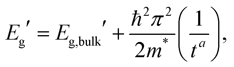 | (1) |
 ) is also shown in Fig. 3b. It agrees well with the present nanosheets behavior, and suggests this observation is related to the anisotropy of the nanoplatelets, with one dimension out of the three being confined as in our NS. The predicted bandgap value from DFT for the single layer (2.93 eV) is slightly higher than the one previously calculated (2.84 eV) assuming a cubic structure.8 The results from Fig. 3b can be used to predict the bandgap values in CsPbBr3 nanosheets as a function of the layer thickness. Unfortunately, ultrathin nanosheets (N ≤ 6) did not survive the deposition on the support films, making EELS acquisitions at the extreme thin end of the thickness range impossible (see ESI† for further details).
 | ||
| Fig. 3 (a) EEL spectrum from a CsPbBr3 nanosheet (N ∼ 50) in the region of the optical bandgap. The black curve is the raw data, and the orange curve is the result after a Savitzky–Golay smooth. The dash black curve is the first derivative of the smoothed curve. The zero-loss (ZL) scaled spectrum used for the precise alignment of the spectra before summation is shown for comparison (blue). (b) Bandgap values calculated from the EELS spectra as a function of the thickness (number of units N) of the CsPbBr3 nanosheets. The measured values are in green. The fit according to the power-law function from eqn (1) is shown (orange line) a function of the number of units N. The curve obtained from DFT simulations is shown in violet, together with values from CsPbBr3 nanostructures as derived from literature. The inset shows an enlargement of the N > 6 part of the plot. | ||
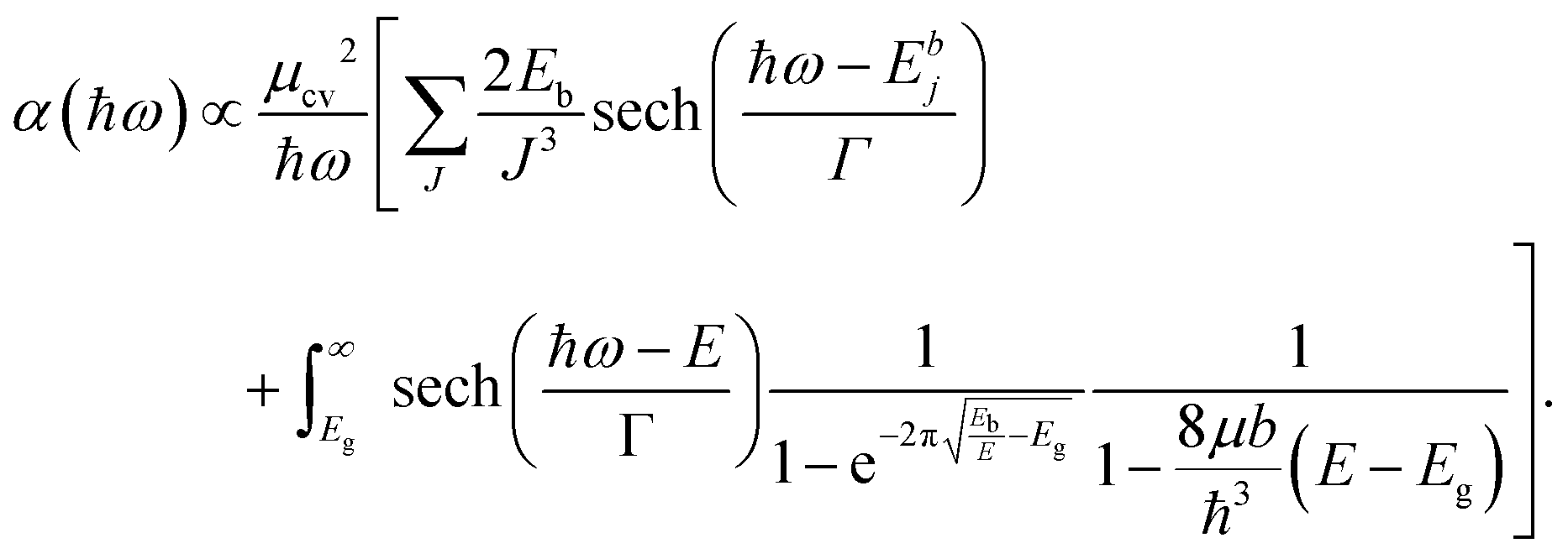
In addition to an estimate of the bandgap, the EEL spectra can also be used to derive other optical properties directly form a single nanostructure. First, the dielectric function ε = ε1 + iε2 can be extracted with a Kramers–Kronig (K–K) analysis,30 using an iterative procedure starting from the energy-loss spectrum after multiple-scattering removal by deconvolution (as the loss function in Fig. S7 in ESI†). To reduce the impact of the surface losses, we restrict our analysis here to the extraction of the dielectric function from a thick nanosheet, and the result is presented in Fig. 4a. In the same figure, the simulated dielectric function from bulk CsPbBr3 calculated from DFT is reported for comparison. Experimental and simulated functions exhibit a similar behavior, confirming again the lack of beam-damage in the experimental data. The most notable difference is the excitonic peak clearly visible in the experiment at ∼2.4 eV, which is not reproducible by single-particle approaches, as in time-dependent density functional theory (TDDFT). The position of the excitonic peak can be used to calculate Eg from Eg′ in eqn (1). However, we need to separate the exciton peak from the continuum of inter-band transitions. This can be done approximately with a fit of the absorption edge44,45 using Elliott's theory,46 which considers a sum of discrete peaks (the Wannier excitons) added to a continuous profile (corrected at finite temperature with the Fermi distribution) for the inter-band transition, and both are convoluted with the spectrum broadening (a combination of excitation life-time and experimental resolution, Γ) according to the following equation (repeated here for clarity from supplementary eqn (9) in ref. 44):
 | (2) |
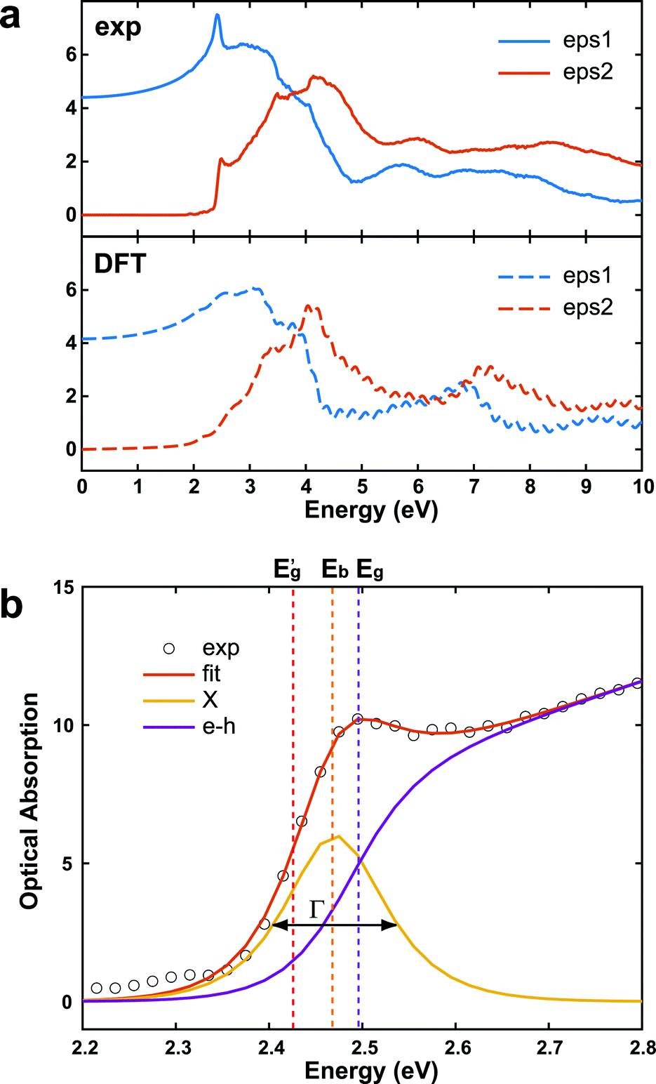 | ||
| Fig. 4 (a) (Upper panel) dielectric function of CsPbBr3 calculated from the experimental EELS spectrum of a thick nanosheet (N ∼ 50) according to the K–K theory, and assuming n(0) ∼ 2.2.43 The simulated dielectric function of bulk CsPbBr3 from DFT is shown for comparison (bottom panel). (b) Enlarged view of the onset region of the corresponding optical absorption spectrum. The inter-band (e–h, purple curve) can be extracted from an Elliott's fit (eqn (2)). The exciton peak centered in Eb (X, orange curve) has a sech shape with broadening Γ (FWHM). (Eb = 0.023 eV, Eg = 2.491 eV, Γ = 0.047 eV). | ||
The interested reader can find in ref. 44 a description of all the parameters. The model can then be fitted to the spectrum to extract both Eg (inter-band gap) and Eb (exciton binding energy). By applying the procedure to the absorption spectrum in Fig. 4b, we obtained an estimation for the exciton binding energy of Eb = 23 meV, in excellent agreement with the literature.44 This results in an offset 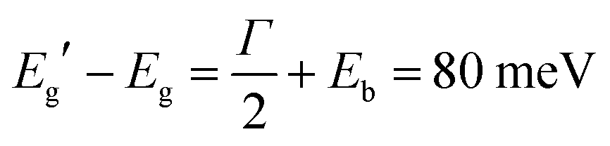 .
.
Conclusions
ADF-STEM images at high resolution have made it possible to determine the structure of CsPbBr3 thin nanosheets. In particular, the Br atomic columns clearly present the rotated octahedral arrangement of the orthorhombic structure.14 No evidence was found of the out of phase rotation of the Br octahedra that would be expected in the tetragonal symmetry, thus confirming our previous hypothesis of a predominantly orthorhombic structure.8 These thin and wide nanosheets are ideal candidates to verify the emergence of a true 1D electronic confinement (in the z direction). The use of 60 kV EELS at high energy resolution (FWHM of the zero-loss peak <20 meV) allowed us to follow the bandgap opening as the CsPbBr3 nanosheets became thinner. The extrapolation of the fit to extreme small thickness shows an overall lower confinement effect with respect to quantum dots and nanoplatelets (3D confinement) reported in literature. The effect of confinement starts to manifest itself at thicknesses below 10 nm, with an inflection point between a low confinement regime and a high confinement regime. A bandgap of 2.446(5) eV at large thickness (bulk) was measured. This corresponds to 2.491(5) eV for the inter-band separation, according to Elliott's theory.Conflicts of interest
There are no conflicts to declare.Acknowledgements
SuperSTEM is the UK National Research Facility for Advanced Electron Microscopy, supported by the Engineering and Physical Research Council (EPSRC). R. B. and G. B. thank Valeria Nicolosi (The Advanced Microscopy Laboratory, CRANN, Trinity College Dublin) for the access to the microscopes.References
- http://www.nrel.gov/pv/assets/images/efficiency-chart.png, accessed July 10th, 2020.
- C. K. Møller, Nature, 1958, 182, 1436 CrossRef.
- D. Z. Weber, Z. Naturforsch. B, 1978, 33b, 1443–1445 CAS.
- D. B. Mitzi, in Progress in Inorganic Chemistry, ed. K. D. Karlin, John Wiley & Sons, Inc., 2007, vol. 48, pp. 1–121 Search PubMed.
- L. C. Schmidt, A. Pertegás, S. González-Carrero, O. Malinkiewicz, S. Agouram, G. Mínguez Espallargas, H. J. Bolink, R. E. Galian and J. Pérez-Prieto, J. Am. Chem. Soc., 2014, 136, 850–853 CrossRef CAS.
- L. Protesescu, S. Yakunin, M. I. Bodnarchuk, F. Krieg, R. Caputo, C. H. Hendon, R. X. Yang, A. Walsh and M. V. Kovalenko, Nano Lett., 2015, 15, 3692–3696 CrossRef CAS.
- Y. Bekenstein, B. A. Koscher, S. W. Eaton, P. Yang and A. P. Alivisatos, J. Am. Chem. Soc., 2015, 137, 16008–16011 CrossRef CAS.
- Q. A. Akkerman, S. G. Motti, A. R. Srimath Kandada, E. Mosconi, V. D’Innocenzo, G. Bertoni, S. Marras, B. A. Kamino, L. Miranda, F. De Angelis, A. Petrozza, M. Prato and L. Manna, J. Am. Chem. Soc., 2016, 138, 1010–1016 CrossRef CAS.
- Y. Yu, D. Zhang, C. Kisielowski, L. Dou, N. Kornienko, Y. Bekenstein, A. B. Wong, A. P. Alivisatos and P. Yang, Nano Lett., 2016, 16, 7530–7535 CrossRef CAS.
- J. Butkus, P. Vashishtha, K. Chen, J. K. Gallaher, S. K. K. Prasad, D. Z. Metin, G. Laufersky, N. Gaston, J. E. Halpert and J. M. Hodgkiss, Chem. Mater., 2017, 29, 3644–3652 CrossRef CAS.
- Q. Wang, X.-D. Liu, Y.-H. Qiu, K. Chen, L. Zhou and Q.-Q. Wang, AIP Adv., 2018, 8, 025108 CrossRef.
- J. Lin, L. Gomez, C. de Weerd, Y. Fujiwara, T. Gregorkiewicz and K. Suenaga, Nano Lett., 2016, 16, 7198–7202 CrossRef CAS.
- R. Erni and N. D. Browning, Ultramicroscopy, 2007, 107, 267–273 CrossRef CAS.
- M. C. Brennan, M. Kuno and S. Rouvimov, Inorg. Chem., 2019, 58, 1555–1560 CrossRef CAS.
- R. dos Reis, H. Yang, C. Ophus, P. Ercius, G. Bizarri, D. Perrodin, T. Shalapska, E. Bourret, J. Ciston and U. Dahmen, Appl. Phys. Lett., 2018, 112, 071901 CrossRef.
- J. Varignon, N. C. Bristowe and P. Ghosez, Phys. Rev. Lett., 2016, 116, 057602 CrossRef.
- F. Bertolotti, G. Nedelcu, A. Vivani, A. Cervellino, N. Masciocchi, A. Guagliardi and M. V. Kovalenko, ACS Nano, 2019, 13, 14294–14307 CrossRef CAS.
- J. C. Dahl, X. Wang, X. Huang, E. M. Chan and A. P. Alivisatos, J. Am. Chem. Soc., 2020, 142, 11915–11926 CrossRef CAS.
- J. Shamsi, Z. Dang, P. Bianchini, C. Canale, F. Di Stasio, R. Brescia, M. Prato and L. Manna, J. Am. Chem. Soc., 2016, 138, 7240–7243 CrossRef CAS.
- Z. Dang, J. Shamsi, F. Palazon, M. Imran, Q. A. Akkerman, S. Park, G. Bertoni, M. Prato, R. Brescia and L. Manna, ACS Nano, 2017, 11, 2124–2132 CrossRef CAS.
- A. D. Backer, K. H. W. van den Bos, W. V. den Broek, J. Sijbers and S. V. Aert, Ultramicroscopy, 2016, 171, 104–116 CrossRef.
- J. Barthel, Ultramicroscopy, 2018, 193, 1–11 CrossRef CAS.
- C. Dwyer, C. Maunders, C. L. Zheng, M. Weyland, P. C. Tiemeijer and J. Etheridge, Appl. Phys. Lett., 2012, 100, 191915 CrossRef.
- H. E, K. E. MacArthur, T. J. Pennycook, E. Okunishi, A. J. D’Alfonso, N. R. Lugg, L. J. Allen and P. D. Nellist, Ultramicroscopy, 2013, 133, 109–119 CrossRef CAS.
- M. Nord, P. E. Vullum, I. MacLaren, T. Tybell and R. Holmestad, Adv. Struct. Chem. Imaging, 2017, 3, 9 CrossRef.
- K. Momma and F. Izumi, J. Appl. Crystallogr., 2011, 44, 1272–1276 CrossRef CAS.
- R. Erni and N. D. Browning, Ultramicroscopy, 2008, 108, 84–99 CrossRef CAS.
- M. Stöger-Pollach, H. Franco, P. Schattschneider, S. Lazar, B. Schaffer, W. Grogger and H. W. Zandbergen, Micron, 2006, 37, 396–402 CrossRef.
- R. F. Egerton, P. Li and M. Malac, Micron, 2004, 35, 399–409 CrossRef CAS.
- R. F. Egerton, Electron Energy-Loss Spectroscopy in the Electron Microscope, Springer, Boston, MA, 2011 Search PubMed.
- J. P. Perdew, K. Burke and M. Ernzerhof, Phys. Rev. Lett., 1997, 78, 1396 CrossRef CAS.
- S. Grimme, J. Comput. Chem., 2006, 27, 1787–1799 CrossRef CAS.
- A. Dal Corso, Comput. Mater. Sci., 2014, 95, 337–350 CrossRef CAS.
- S. Van Aert, J. Verbeeck, R. Erni, S. Bals, M. Luysberg, D. V. Dyck and G. V. Tendeloo, Ultramicroscopy, 2009, 109, 1236–1244 CrossRef CAS.
- A. De Wael, A. De Backer, L. Jones, P. D. Nellist and S. Van Aert, Ultramicroscopy, 2017, 177, 69–77 CrossRef CAS.
- C. C. Stoumpos, C. D. Malliakas, J. A. Peters, Z. Liu, M. Sebastian, J. Im, T. C. Chasapis, A. C. Wibowo, D. Y. Chung, A. J. Freeman, B. W. Wessels and M. G. Kanatzidis, Cryst. Growth Des., 2013, 13, 2722–2727 CrossRef CAS.
- G. Bertoni, Q. Ramasse, R. Brescia, L. De Trizio, F. De Donato and L. Manna, ACS Mater. Lett., 2019, 1, 665–670 CrossRef CAS.
- K. Iakoubovskii, K. Mitsuishi, Y. Nakayama and K. Furuya, Microsc. Res. Tech., 2008, 71, 626–631 CrossRef CAS.
- H.-R. Zhang, R. F. Egerton and M. Malac, Micron, 2012, 43, 8–15 CrossRef CAS.
- P. Yu and M. Cardona, Fundamentals of Semiconductors, Springer-Verlag Berlin Heidelberg, 2010 Search PubMed.
- H. M. Ghaithan, Z. A. Alahmed, S. M. H. Qaid, M. Hezam and A. S. Aldwayyan, ACS Omega, 2020, 5, 7468–7480 CrossRef CAS.
- M. C. Brennan, J. E. Herr, T. S. Nguyen-Beck, J. Zinna, S. Draguta, S. Rouvimov, J. Parkhill and M. Kuno, J. Am. Chem. Soc., 2017, 139, 12201–12208 CrossRef CAS.
- D. N. Dirin, I. Cherniukh, S. Yakunin, Y. Shynkarenko and M. V. Kovalenko, Chem. Mater., 2016, 28, 8470–8474 CrossRef CAS.
- M. Saba, M. Cadelano, D. Marongiu, F. Chen, V. Sarritzu, N. Sestu, C. Figus, M. Aresti, R. Piras, A. Geddo Lehmann, C. Cannas, A. Musinu, F. Quochi, A. Mura and G. Bongiovanni, Nat. Commun., 2014, 5, 5049 CrossRef CAS.
- F. Ruf, A. Magin, M. Schultes, E. Ahlswede, H. Kalt and M. Hetterich, Appl. Phys. Lett., 2018, 112, 083902 CrossRef.
- R. J. Elliott, Phys. Rev., 1957, 108, 1384–1389 CrossRef CAS.
Footnotes |
| † Electronic supplementary information (ESI) available. See DOI: 10.1039/d0nh00477d |
| ‡ Present address: Cavendish Laboratory, University of Cambridge, 19 JJ Thomson Avenue, Cambridge CB3 0HE, UK. |
| This journal is © The Royal Society of Chemistry 2020 |