
 Open Access Article
 This Open Access Article is licensed under a
 Creative Commons Attribution 3.0 Unported Licence
Directional ultrafast charge transfer in a WSe2/MoSe2 heterostructure selectively probed by time-resolved SHG imaging microscopy†
Jonas E.
Zimmermann
a,
Young Duck
Kim‡
b,
James C.
Hone
b,
Ulrich
Höfer
a and
Gerson
Mette
 *a
*a
aFachbereich Physik, Philipps-Universität Marburg, Marburg D-35032, Germany. E-mail: gerson.mette@physik.uni-marburg.de
bDepartment of Mechanical Engineering, Columbia University, New York 10027, USA
First published on 21st October 2020
Abstract
Heterostructures of two-dimensional transition metal dichalcogenides (TMD) have shown promise for various optoelectronic and novel valleytronic applications. Due to their type-II band alignment, photoexcited electrons and holes can separate into different layers through ultrafast charge transfer. While this charge-transfer process is critical for potential applications, the underlying mechanisms still remain elusive. Here, we demonstrate for a rotationally mismatched WSe2/MoSe2 heterostructure that directional ultrafast charge transfer between the layers becomes accessible by time-resolved optical second-harmonic generation. By tuning the photon energy of the pump pulse, one of the two materials is resonantly excited, whereas the polarization of the probe pulse can be optimized to selectively detect the charge transfer into the other material. This allows us to explore the interlayer hole transfer from the WSe2 into the MoSe2 layer and vice versa, which appears within a few hundred femtoseconds via hybridized intermediate states at the Γ-point. Our approach enables systematic investigations of the charge transfer in dependence of the rotational layer mismatch in TMD heterostructures.
New conceptsHeterostructures of transition metal dichalcogenides (TMD) feature a type-II band alignment which can separate photoexcited electrons and holes into different layers through ultrafast charge transfer and can host long-lived interlayer excitons due to their spatially indirect nature. While this charge transfer is essential for potential applications, the underlying mechanisms still remain elusive. The main drawbacks of previous approaches were insufficient time-resolution of the employed microscopy setups and deficiencies of linear optical spectroscopies to address individual layers of the heterostructure selectively. We introduce a new experimental concept for investigating ultrafast charge-transfer processes in TMD heterostructures by means of optical pump second-harmonic probe microscopy. Our technique combines the advantages of time-resolved optical second-harmonic generation (SHG) with an optical microscopy setup. On the one hand, the method allows for pump–probe experiments in μm small structures with a superior time-resolution. On the other hand, the tensorial nature of the second-order nonlinear susceptibility allows us to distinguish the response from differently oriented layers to elucidate directional interlayer charge transfer as demonstrated for a rotationally mismatched WSe2/MoSe2 heterostructure. Thus, by combining polarization- and time-resolved measurements, very clear and systematic experiments can be performed for a variety of heterostructures to correlate observed transient changes with the underlying structure. |
Van-der-Waals coupled 2D materials feature fascinating opportunities for designing stacked heterostructures.1,2 In particular, heterostructures of transition metal dichalcogenides (TMDs) have shown promise for various optoelectronic and valleytronic applications.3,4 Several combinations of TMDs in a heterobilayer reveal a type-II band alignment resulting in spatially separated electron–hole pairs after optical excitation (so called charge-transfer or interlayer excitons).5–12 Beside the choice of the materials, the relative orientation of the stacked layers can affect the interlayer coupling and the properties of the interlayer excitons.13–20 Rotational misfit between two TMD monolayers results in a corresponding rotation of the hexagonal Brillouin zones and momentum-mismatched interlayer excitations. Therefore, the stacking should considerably influence the ultrafast charge transfer as well as the interlayer recombination following an optical excitation. Accordingly, a distinct difference in the exciton recombination of coherently and randomly stacked MoS2/WS2 heterostructures has been observed.21 Systematic measurements on MoS2/WSe2 heterostructures, however, exhibit strong variations of the charge-recombination lifetime from sample to sample but no clear correlation with the twist angle.22 With respect to the ultrafast charge transfer, recent experimental studies obtained surprisingly diverse results. For MoS2/WSe2 heterostructures, the initial charge transfer was reported to be faster than the experimental time resolution of 40 fs independent of the examined stacking angles.22 In contrast, much slower transfer times of a few hundred femtoseconds and a significant increase for larger rotational mismatch were observed for a WS2/WSe2 interface.23
Thus, despite the recent progress in the study of ultrafast dynamics in TMD heterostructures, the underlying mechanism for the charge-transfer process still remains elusive.24 In this work, we therefore introduce a new experimental concept for the investigation of ultrafast charge transfer in TMD heterostructures by means of time-resolved optical second-harmonic generation (SHG). Our SHG imaging microscopy technique can overcome the main drawbacks of previous experimental approaches which were insufficient time-resolution of the employed microscopy setups and deficiencies to address pump-induced changes in a particular layer of the heterostructure selectively. Thus, in the commonly used linear pump–probe spectroscopy the measured transient response consists of a superposition of monolayer and heterostructure contributions. Furthermore, charge transfer can appear in both directions simultaneously depending on the excitation energy. Here, we demonstrate for the example of a rotationally mismatched WSe2/MoSe2 heterostructure that directional ultrafast charge transfer between the layers becomes accessible. By tuning the photon energy of the pump pulse, we can resonantly excite one of the two materials, whereas the polarization of the probe pulse allows us to selectively detect the charge transfer in the other material. The observed hole transfer times differ considerably for the opposite directions: from the WSe2 into the MoSe2 layer (and vice versa) charge transfer appears within 610 ± 150 fs (210 ± 60 fs) as determined from our second-harmonic (SH) transients. Furthermore, our results indicate that the charge transfer takes place via hybridized intermediate states at the Γ-point.
The applied SHG imaging microscopy technique, illustrated in Fig. S1 of the ESI,† combines the advantages of time-resolved SHG with an optical microscopy setup. It allows pump–probe experiments with an ideal time-resolution only limited by the used laser system to explore ultrafast dynamical changes in μm small structures. Since the SHG process is described by a third-rank tensor in the electric-dipole approximation, it has been established as a sensitive optical probe of the crystal orientation in TMD monolayers25–27 or for the stacking angle in heterostructures.28 By combination of polarization- and time-resolved measurements, very clear and systematic measurements can be performed to correlate the observed transient changes in the SH response with the underlying structure. The studied heterostructure consists of two stacked TMD monolayers (WSe2/MoSe2) encapsulated between thick layers of hexagonal boron nitride (hBN) for environmental protection.29 The heterostructure was fabricated by using a stamp of polydimethylsiloxane elastomer to stack the different materials consecutively, starting with the hBN top-layer, followed by the WSe2 monolayer and the MoSe2 monolayer. This stack was then finally put onto the hBN bottom-layer which was exfoliated on SiO2/Si(001). This polymer-free layer assembly enables fabrication of ultraclean interfaces without contamination of interfaces by polymer or solvent.29,30 An optical microscopy image of the final stack is shown in Fig. 1(a). The various mono- and multilayer flakes in combination with observable cracks and wrinkles make a clear identification of the individual layers rather difficult. Therefore, Fig. 1(b) displays a detail of (a) with the individual WSe2 and MoSe2 layers highlighted with dashed and dotted lines, respectively. Thus, the actual WSe2/MoSe2 heterostructure region is visualized by the marked red area. Details about the structural characterization of the WSe2/MoSe2 heterostructure can be found in the ESI.†
 | ||
| Fig. 1 (a) Optical microscopy image of the studied hBN/WSe2/MoSe2/hBN heterostructure. The dashed square represents the area shown in (b). Two visible wrinkles are marked by black arrows. Bottom and top hBN flakes are highlighted by dot-dashed and dotted lines, respectively. (b) Detail of the microscopy image in (a) highlighting the MoSe2 and WSe2 monolayer flake edges by dotted and dashed lines, respectively. The area within the red line represents the actual heterostructure. (c and d) SHG microscopy images for the polarization angles I and II which correspond to the intensity maxima of MoSe2 and WSe2 layers as shown in (e). The SH response agrees very well with the shape of the individual monolayer flakes as obtained from (b). All scalebars denote 10 μm. (e) Polarization dependent SH data evaluated from the MoSe2 monolayer (blue), the WSe2 monolayer (green) and the heterostructure (red) regions. Blue and green solid lines are the corresponding fits from which the crystal orientations of the MoSe2 and WSe2 monolayer are extracted. The polarization dependence of the heterostructure can be described by a superposition of the electric field components generated by the two monolayers (red solid line). The time-resolved SHG measurements shown in Fig. 2 were performed at probe polarization III. | ||
Fig. 1(e) displays the second-harmonic response in dependence of the polarization ϕ of the 800 nm probe laser evaluated for the MoSe2 monolayer (blue), the WSe2 monolayer (green) and the WSe2/MoSe2 heterostructure (red) regions. As discussed above, we can utilize the rotational anisotropy of SHG in TMD monolayers to determine the crystal orientation of the individual flakes.25–27 For p-polarized SH light and normal incidence of the probe beam, the polarizational anisotropy from the monolayers can be described by a cos(2ϕ + 3Ψ)-dependence, where ϕ = 0° corresponds to p-polarized incoming light and Ψ is the angle between the armchair direction of the crystal and the horizontal.31 In our case of a small angle of incidence, the expected two-fold symmetry is broken and two pairs of maxima with different heights are observed.31 From the corresponding fits (solid lines) to the polarization dependence of the monolayer flakes, the crystal orientations with respect to the horizontal are determined to be 2.1° and 34.4° for the WSe2 and the MoSe2 monolayer, respectively. From this, a stacking angle of 32.3° for the heterostructure can be deduced. By tuning the polarization of the probe laser to an intensity maximum of a specific monolayer, one can visualize the shape of the respective flake in the SHG microscopy image. As shown in Fig. 1(c) and (d), the SH images at polarization I and II nicely reproduce the contours of the MoSe2 and the WSe2 monolayer, respectively. The SH response of the individual monolayers clearly exhibits spatial inhomogeneity within each flake. In particular the intensity along the visible diagonal wrinkles marked by arrows in Fig. 1(a) is strongly reduced for both polarizations. Despite this spatial inhomogeneity of the absolute SH signal, the normalized pump-induced changes in the SH response are comparatively homogeneous as can be seen for example in Fig. 2(b).
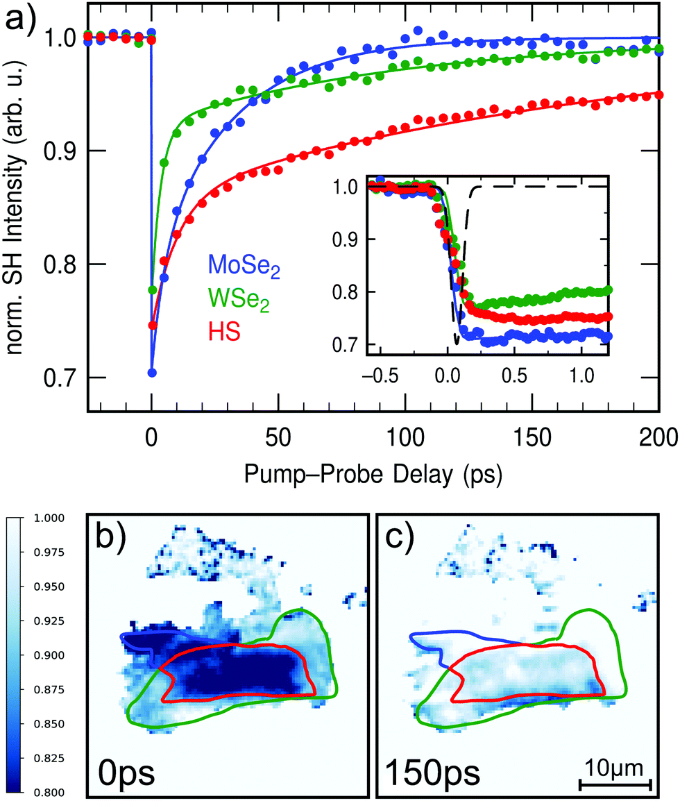 | ||
| Fig. 2 Time-resolved SHG of the WSe2/MoSe2 heterostructure upon 2.09 eV optical excitation measured with probe polarization III. (a) Averaged SH intensities of the heterostructure and monolayer regions in dependence of the pump–probe delay. The inset shows the SH transients around temporal overlap measured with higher resolution. The cross correlation of the laser pulses corresponds to the black line. (b and c) Show normalized SH images at two different pump–probe delays of 0 ps and 150 ps, respectively. The SH response of the heterostructure exhibits significant differences compared with the two monolayer signals. At first, the three signals show a pump-induced ultrafast decrease of the SH intensity. However, while the monolayer signals begin to recover immediately after the optical excitation, a delayed decrease in SH intensity occurs in the heterostructure within several hundred femtoseconds after temporal overlap (inset). Furthermore, the subsequent relaxation of the heterostructure signal is considerably slower than for the monolayers. | ||
In order to investigate the ultrafast charge transfer in the heterostructure, the pump-induced change of the SH response in dependence of the pump–probe delay is studied. At a probe polarization of 110°, decent SH intensity can be obtained from the heterostructure and both monolayers [cf. polarization III in Fig. 1(e)]. Time-resolved SHG measurements upon 593 nm excitation for this particular probe polarization are shown in Fig. 2. At this pump–photon energy (2.09 eV) the B-exciton of WSe2 is resonantly excited.32Fig. 2(a) represents the averaged SH intensities of the heterostructure (red) as well as WSe2 (green) and MoSe2 (blue) monolayers in dependence of the pump–probe delay. The transients are normalized to the signal at negative delay, i.e. before arrival of the pump–pulse, and therefore show the relative intensity changes in %. Normalized SHG microscopy images at two different pump–probe delays of 0 ps and 150 ps in Fig. 2(b) and (c) visualize the pump-induced changes within the different regions of the structure. A complete movie of the time-resolved SHG microscopy measurements can be found in the ESI.† The transient SH response of the heterostructure exhibits significant differences when compared with the two monolayer signals. At temporal overlap, all three signals show a pump-induced ultrafast decrease of the SH intensity. After the optical excitation, the monolayer signals begin to recover immediately. In the heterostructure, however, there is a continued/delayed decrease in SH intensity occurring within several hundred femtoseconds after temporal overlap as shown in the inset of Fig. 2(a). Additionally, the subsequent relaxation of the heterostructure signal for large pump–probe delays is considerably slower than for the monolayers [Fig. 2(a)]. The transients of the heterostructure and the monolayers can be described by a bi-exponential decay. The corresponding lifetimes τ1 and τ2 as determined from a rate-equation model correspond to 5 ps and 32 ps for MoSe2, 7 ps and 102 ps for WSe2, and 19 ps and 203 ps for the heterostructure.
We attribute the fast initial decrease of the SH response to pump-induced changes in the second-order nonlinear susceptibility of the TMD monolayers, e.g., due to depopulation of the valence band associated with the generation of intralayer excitons.31 The subsequent progression as observable in the monolayer transients is then interpreted as exciton relaxation. In the heterostructure, ultrafast charge transfer between the layers can lead to the generation of spatially separated interlayer excitons. Accordingly, photoluminescence measurements on the very same heterostructure revealed characteristic emission from interlayer excitons at 1.4 eV.33 We therefore assign the continued decrease of the SH signal in the heterostructure within the first picosecond to the delayed formation of those charge-transfer excitons. Due to the reduced spatial overlap of electron- and hole-wavefunctions the interlayer excitons reveal an enhanced lifetime in accordance with our findings.10
The particular advantage of time-resolved second-harmonic generation to investigate the ultrafast charge transfer in TMD heterostructures is the intrinsic sensitivity of SHG on the crystal symmetry. By tuning the probe polarization we can, thus, enhance the sensitivity for a particular layer in the heterostructure. Fig. 3 shows a polarizational anisotropy measurement of the SH response obtained from the heterostructure region upon optical excitation at 2.09 eV. At negative delays, i.e. without any influence of the pump beam, the same anisotropy as in Fig. 1 is observed for the heterostructure [cf. empty dots in Fig. 3(a)]. At a positive delay of 1.5 ps, however, the heterostructure signal is considerably reduced due to the fast initial decrease induced by the pump pulse [cf. filled dots in Fig. 3(a)]. Clearly, the absolute change of the SH response represented by the difference of the two data sets [cf. crosses in Fig. 3(a)] exhibits a striking anisotropy, which becomes even more apparent when this absolute difference Δ is divided by the SH response at negative delays for each polarization angle. The resulting signal shown in Fig. 3(b) represents the relative pump-induced change δ of the SH signal which reveals a two-fold symmetric polarization dependence with strong pump-induced decrease of the SH signal by up to 75%. Our finding implies that the size of the pump-induced effect depends on the polarization of the probe laser, which at first glance might seem implausible. Closer examination, however, shows that the greatest pump influence occurs exactly when the probe polarization is tuned to the intensity maximum of the MoSe2 monolayer (cf. polarization I in Fig. 1 and 3). Corresponding SHG microscopy images shown in Fig. S3 of the ESI† furthermore illustrate that this strong polarization dependence on the pump-induced effect only appears in the heterostructure while the respective decrease in the monolayers is basically constant for all polarization angles. Our results thus reveal, that for resonant excitation of the WSe2 monolayer at 2.09 eV, the detection efficiency for interlayer charge transfer is the highest when the probe polarization is most sensitive to the MoSe2 monolayer. This allows us to selectively study directional differences of the ultrafast charge transfer in TMD heterostructures as we will show in the following.
 | ||
| Fig. 3 (a) Polarizational anisotropy measurements of the SH response obtained from the WSe2/MoSe2 heterostructure upon 2.09 eV excitation for two different pump–probe delays of −1.5 ps (empty dots) and +1.5 ps (filled dots), i.e. before and after temporal overlap. The difference of the two data sets (crosses) displays the absolute change Δ of the SH signal in dependence of the probe polarization. (b) The relative pump-induced change δ obtained by dividing the absolute change by the SH response at negative delays exhibits a striking anisotropy. The pump-induced decrease of the SH signal is found to vary between ≈20% and ≈75%. | ||
Applying our time- and polarization-resolved SHG microscopy technique in combination with pump–photon energy dependent measurements reveals a very clear picture of the ultrafast charge-transfer process in the WSe2/MoSe2 heterostructure. Fig. 4 shows time-resolved SH measurements for two pump–photon energies and two different probe polarizations. The chosen excitation energies are 2.09 eV (Fig. 4(a)) and 1.80 eV (Fig. 4(c)), resonant to the B-excitons of WSe2 and MoSe2, respectively. The polarizations are selected in order to enhance the sensitivity to an individual layer in the heterostructure. As shown in Fig. 4(a) for resonant excitation of WSe2, the normalized SH signal of the heterostructure exhibits significant differences for the two probe polarizations. Thus, the delayed decrease of the SH signal which was associated with ultrafast interlayer charge transfer is observed only for probe polarization I sensitive to the MoSe2 layer. In contrast, the heterostructure signal measured at polarization II exhibits no delayed decrease but very similar dynamics as obtained from the WSe2 monolayer. The opposite behavior is found for resonant excitation of MoSe2 shown in Fig. 4(c). Here, the delayed decrease in the heterostructure transient is only observed for probe polarization II. Surprisingly, the heterostructure transient for resonant excitation of the A-excitons of WSe2 at 1.70 eV shows no indication of any charge transfer as shown in Fig. S4 and S5(a) in the ESI.† In contrast, non-resonant excitation of the MoSe2 A-excitons using the same photon energy shows a weak signature for charge transfer into the WSe2 monolayer [cf. Fig. S5(b), ESI†]. In the case of resonant excitation of the WSe2 A-exciton (1.68 eV), one would expect solely electron transfer into MoSe2. Our results thus suggest, that this process is either not feasible or faster than our experimental time-resolution, estimated to be ≈15 fs (1/5th of the cross correlation FWHM). However, due to the large lattice mismatch of the layers in the studied heterostructure, the latter seems less likely. In order to describe the observed dynamics in the heterostructure quantitatively, we have applied a rate-equation model which takes a delayed filling by interlayer charge transfer into account as discussed in the ESI.† From this model, the transfer times for charge transfer from WSe2 into MoSe2 (τWSe2→MoSe2 = 610 ± 150 fs) and vice versa (τMoSe2→WSe2 = 210 ± 60 fs) were extracted. The corresponding fits are shown as solid lines in Fig. 4(a) and (c).
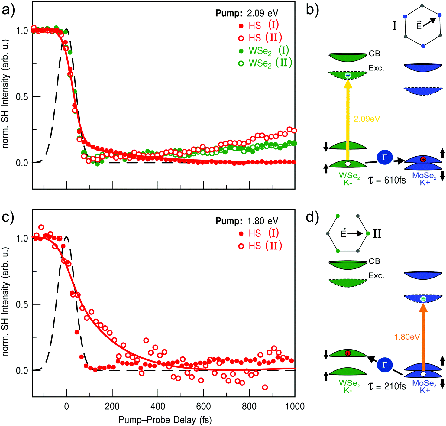 | ||
| Fig. 4 Time-resolved SHG of the WSe2/MoSe2 heterostructure for two different pump–photon energies and two different probe polarizations. All SH transients are normalized, first to the signal at negative delays and then to the maximal pump-induced decrease for easier comparison of the dynamical changes. (a) SH transients for 2.09 eV pump–photon energy, resonant with the WSe2 B-exciton. Filled and unfilled red data points correspond to the heterostructure signal with the probe polarization sensitive to MoSe2 and WSe2, respectively. A delayed decrease of the SH signal associated with ultrafast interlayer charge transfer is only observed for probe polarization I sensitive to the MoSe2 layer. For probe polarization II, however, the transient of the heterostructure signal (unfilled) exhibits the very same dynamics as obtained from the WSe2 monolayer (green). (b) Schematic drawing of the charge transfer into the MoSe2 following resonant optical excitation of WSe2 probed by polarization I. (c) SH transients like in (a) but for 1.80 eV pump–photon energy, resonant with the MoSe2 B-exciton. Contrary to (a), the delayed decrease of the SH signal due to the interlayer charge transfer is only observed for probe polarization II sensitive to the WSe2 layer. (d) Schematic drawing of the charge transfer into the WSe2 following resonant optical excitation of MoSe2 probed by polarization II. Solid lines in (a and c) correspond to a rate-equation fit to extract the interlayer transfer times. The cross correlation of the laser pulses is shown as a black line. | ||
It has been proposed that intermediate states outside the K-valleys play a central role for the charge transfer in momentum-mismatched TMD heterostructures.8,34–38 Band structure calculations show that conduction band states at the Σ-point shift energetically below the K-point minimum for certain stacking angles.34 These states show strong hybridization of the individual wavefunctions of the monolayers,34,35,37 and therefore enable a more efficient interlayer transfer. Further evidence for this process is given by two-photon photoemission measurements on bulk MoS2, where ultrafast charge transfer to the Σ-point has been observed,39 underlining the strong influence these states may have on the charge transfer in heterostructures. Since there is no experimental evidence for electron transfer from our energy-dependent measurements, we thus interpret the observed delayed filling as hole transfer between the layers assisted by hybridized states around the Γ-point as illustrated in Fig. 4(b) and (d). Further evidence for this attribution is given by systematic measurements changing the pump–photon energy successively to explore the charge transfer from WSe2 to MoSe2 in more detail. Here, the pump-induced decrease of the SH intensity shows a clear resonance around the B-exciton energy of WSe2 as shown in Fig. S4 of the ESI.† Furthermore, ultrafast charge transfer to MoSe2 is only observed for excitation energies equal to or higher than the WSe2 B-exciton resonance. From bandstructure calculations it is known that the Γ-point in the heterostructure is energetically located between the valence band maxima of the individual monolayers.34,37 After their generation the excitons can access multiple relaxation routes. Within the monolayer, intra-valley scattering from B- to A-excitons is spin forbidden, but scattering from the K+ to the K− valleys is allowed. In direct competition to this process is the interlayer transfer observed in our measurements, e.g. from the MoSe2 K+ to WSe K− valley or vice versa as illustrated in Fig. 4(b) and (d).
Similarly, our measurements also indicate ultrafast hole transfer from the MoSe2 K+ to WSe2 K+ valley after optical excitation of MoSe2 A-excitons as shown in Fig. S5(b) of the ESI.† However, there is no experimental evidence for electron transfer from WSe2 to MoSe2 after resonant excitation of WSe2 A-excitons [cf. Fig. S5(a), ESI†]. As discussed above, this result suggests that electron transfer in our heterostructure is either faster than the experimental time-resolution or not feasible due to the relatively large stacking angle. Of course, the charge transfer could also be so slow or inefficient, that its particular signature is superimposed by the faster monolayer dynamics. A recent study of a WS2/WSe2 heterostructure has observed electron transfer occurring within 200 fs and 1.2 ps after resonant excitation of WSe2 A-excitons depending on the rotational mismatch.23 While the order of magnitude compares reasonably well with our extracted transfer times for interlayer hole transfer, the question remains why electron transfer is not observable for our particular heterostructure. To further elucidate possible charge-transfer mechanisms in TMD heterostructures, stacking-dependent measurements have to be performed systematically for different material combinations. Our results demonstrate that the introduced SHG imaging microscopy technique is ideally suited for such systematic investigations of the ultrafast dynamics in momentum-mismatched TMD heterostructures. Those measurements would be further improved by an extended tuning range for the pump–photon energies to access all the exciton resonances of a certain heterostructure sample. In addition, a wavelength-tunable probe beam could further enhance the sensitivity for charge transfer into a certain material by making use of a resonant enhancement of the SH process.
In conclusion, we have introduced time-resolved SHG imaging microscopy for the investigation of ultrafast charge transfer in heterostructures of two-dimensional transition metal dichalcogenides. This method combines superior time-resolution with layer-sensitive detection and in situ determination of stacking angles. For a rotationally mismatched WSe2/MoSe2 heterostructure, our polarization- and energy-dependent measurements reveal directional interlayer hole transfer from the WSe2 into the MoSe2 layer and vice versa, which appears in both cases within a few hundred femtoseconds. These results demonstrate that our approach enables systematic investigations of the charge transfer in dependence of the rotational layer mismatch in TMD heterostructures.
Methods
The experiments were performed under ambient conditions using 50 fs laser pulses generated by a femtosecond Ti:sapphire laser amplifier system (Coherent RegA 9050) operating at 800 nm center wavelength with a repetition rate of 150 kHz. The main part of the amplifier output (90%) is used to pump an optical parametric amplifier (OPA) operating in the visible range. The output of the OPA is compressed by a pair of LaFN28 Brewster prisms. The remaining part of the amplifier output (10%) is focused on the sample to probe the SH response. Both beams are nearly collinear and have an angle of incidence of about 18°. After passing a 400 nm dielectric filter, the specular reflected SH response of the probe beam is imaged optically magnified by a camera lens (Nikon Nikkor, 1![[thin space (1/6-em)]](https://www.rsc.org/images/entities/char_2009.gif) :1.4 ED, f = 50 mm) on an electron-multiplied CCD chip (Princeton Instruments ProEM-HS). Typical exposure times were between 20 and 60 seconds. The applied magnification was M ≈ 35–40. The overall resolution of our imaging microscopy setup is better than 4 μm. The time-delay between pump and probe beam is varied by a motorized delay stage. The polarization of the pump and probe beam can be varied by means of λ/2-plates. The typically detected p-polarization of the second-harmonic light is separated by an analyzer. A combination of λ/2-plate and polarizer enable the continuous variation of the applied pump fluence in the range from 30–150 μJ cm−2 on the sample. The applied probe fluence was fixed to 220 μJ cm−2. Long term measurements with these fluences applied did not exhibit any multishot damage.
:1.4 ED, f = 50 mm) on an electron-multiplied CCD chip (Princeton Instruments ProEM-HS). Typical exposure times were between 20 and 60 seconds. The applied magnification was M ≈ 35–40. The overall resolution of our imaging microscopy setup is better than 4 μm. The time-delay between pump and probe beam is varied by a motorized delay stage. The polarization of the pump and probe beam can be varied by means of λ/2-plates. The typically detected p-polarization of the second-harmonic light is separated by an analyzer. A combination of λ/2-plate and polarizer enable the continuous variation of the applied pump fluence in the range from 30–150 μJ cm−2 on the sample. The applied probe fluence was fixed to 220 μJ cm−2. Long term measurements with these fluences applied did not exhibit any multishot damage.
Conflicts of interest
There are no conflicts to declare.Acknowledgements
We thank D. Günder and G. Witte for structural characterization of our sample by atomic force microscopy. Funding was provided by the Deutsche Forschungsgemeinschaft (DFG, German Research Foundation), Project-ID 223848855-SFB 1083.Notes and references
- A. K. Geim and I. V. Grigorieva, Nature, 2013, 499, 419–425 CrossRef CAS.
- H. Lim, S. I. Yoon, G. Kim, A. R. Jang and H. S. Shin, Chem. Mater., 2014, 26, 4891–4903 CrossRef CAS.
- K. F. Mak and J. Shan, Nat. Photonics, 2016, 10, 216–226 CrossRef CAS.
- X. D. Xu, W. Yao, D. Xiao and T. F. Heinz, Nat. Phys., 2014, 10, 343–350 Search PubMed.
- E. V. Calman, L. H. Fowler-Gerace, D. J. Choksy, L. V. Butov, D. E. Nikonov, I. A. Young, S. Hu, A. Mishchenko and A. K. Geim, Nano Lett., 2020, 20, 1869–1875 CrossRef CAS.
- S. Ovesen, S. Brem, C. Linderalv, M. Kuisma, T. Korn, P. Erhart, M. Selig and E. Malic, Commun. Phys., 2019, 2, 23 CrossRef.
- P. Rivera, H. Yu, K. L. Seyler, N. P. Wilson, W. Yao and X. Xu, Nat. Nanotechnol., 2018, 13, 1004–1015 CrossRef CAS.
- B. Miller, A. Steinhoff, B. Pano, J. Klein, F. Jahnke, A. Holleitner and U. Wurstbauer, Nano Lett., 2017, 17, 5229–5237 CrossRef CAS.
- J. R. Schaibley, P. Rivera, H. Y. Yu, K. L. Seyler, J. Q. Yan, D. G. Mandrus, T. Taniguchi, K. Watanabe, W. Yao and X. D. Xu, Nat. Commun., 2016, 7, 13747 CrossRef CAS.
- P. Rivera, J. R. Schaibley, A. M. Jones, J. S. Ross, S. F. Wu, G. Aivazian, P. Klement, K. Seyler, G. Clark, N. J. Ghimire, J. Q. Yan, D. G. Mandrus, W. Yao and X. D. Xu, Nat. Commun., 2015, 6, 6242 CrossRef CAS.
- H. Fang, C. Battaglia, C. Carraro, S. Nemsak, B. Ozdol, J. S. Kang, H. A. Bechtel, S. B. Desai, F. Kronast, A. A. Unal, G. Conti, C. Conlon, G. K. Palsson, M. C. Martin, A. M. Minor, C. S. Fadley, E. Yablonovitch, R. Maboudian and A. Javey, Proc. Natl. Acad. Sci. U. S. A., 2014, 111, 6198–6202 CrossRef CAS.
- X. P. Hong, J. Kim, S. F. Shi, Y. Zhang, C. H. Jin, Y. H. Sun, S. Tongay, J. Q. Wu, Y. F. Zhang and F. Wang, Nat. Nanotechnol., 2014, 9, 682–686 CrossRef CAS.
- P. Merkl, F. Mooshammer, S. Brem, A. Girnghuber, K.-Q. Lin, L. Weigl, M. Liebich, C.-K. Yong, R. Gillen, J. Maultzsch, J. M. Lupton, E. Malic and R. Huber, Nat. Commun., 2020, 11, 2167 CrossRef CAS.
- P. K. Gogoi, Y. C. Lin, R. Senga, H. P. Komsa, S. L. Wong, D. Z. Chi, A. V. Krasheninnikov, L. J. Li, M. B. H. Breese, S. J. Pennycook, A. T. S. Wee and K. Suenaga, ACS Nano, 2019, 13, 9541–9550 CrossRef CAS.
- J. Kunstmann, F. Mooshammer, P. Nagler, A. Chaves, F. Stein, N. Paradiso, G. Plechinger, C. Strunk, C. Schüller, G. Seifert, D. R. Reichman and T. Korn, Nat. Phys., 2018, 14, 801–805 Search PubMed.
- W. T. Hsu, L. S. Lu, P. H. Wu, M. H. Lee, P. J. Chen, P. Y. Wu, Y. C. Chou, H. T. Jeng, L. J. Li, M. W. Chu and W. H. Chang, Nat. Commun., 2018, 9, 1356 Search PubMed.
- P. C. Yeh, W. Jin, N. Zaki, J. Kunstmann, D. Chenet, G. Arefe, J. T. Sadowski, J. I. Dadap, P. Sutter, J. Hone and R. M. Osgood, Nano Lett., 2016, 16, 953–959 CrossRef CAS.
- S. J. Zheng, L. F. Sun, X. H. Zhou, F. C. Liu, Z. Liu, Z. X. Shen and H. J. Fan, Adv. Opt. Mater., 2015, 3, 1600–1605 CrossRef CAS.
- K. H. Liu, L. M. Zhang, T. Cao, C. H. Jin, D. A. Qiu, Q. Zhou, A. Zettl, P. D. Yang, S. G. Louie and F. Wang, Nat. Commun., 2014, 5, 4966 CrossRef CAS.
- S. X. Huang, X. Ling, L. B. Liang, J. Kong, H. Terrones, V. Meunier and M. S. Dresselhaus, Nano Lett., 2014, 14, 5500–5508 CrossRef CAS.
- H. Heo, J. H. Sung, S. Cha, B. G. Jang, J. Y. Kim, G. Jin, D. Lee, J. H. Ahn, M. J. Lee, J. H. Shim, H. Choi and M. H. Jo, Nat. Commun., 2015, 6, 7372 CrossRef CAS.
- H. M. Zhu, J. Wang, Z. Z. Gong, Y. D. Kim, J. Hone and X. Y. Zhu, Nano Lett., 2017, 17, 3591–3598 CrossRef CAS.
- P. Merkl, F. Mooshammer, P. Steinleitner, A. Girnghuber, K. Q. Lin, P. Nagler, J. Holler, C. Schüller, J. M. Lupton, T. Korn, S. Ovesen, S. Brem, E. Malic and R. Huber, Nat. Mater., 2019, 18, 691–696 CrossRef CAS.
- C. H. Jin, E. Y. Ma, O. Karni, E. C. Regan, F. Wang and T. F. Heinz, Nat. Nanotechnol., 2018, 13, 994–1003 CrossRef CAS.
- Y. Li, Y. Rao, K. F. Mak, Y. You, S. Wang, C. R. Dean and T. F. Heinz, Nano Lett., 2013, 13, 3329–3333 CrossRef CAS.
- N. Kumar, S. Najmaei, Q. Cui, F. Ceballos, P. M. Ajayan, J. Lou and H. Zhao, Phys. Rev. B: Condens. Matter Mater. Phys., 2013, 87, 161403 CrossRef.
- L. M. Malard, T. V. Alencar, A. P. M. Barboza, K. F. Mak and A. M. de Paula, Phys. Rev. B: Condens. Matter Mater. Phys., 2013, 87, 201401 CrossRef.
- W.-T. Hsu, Z.-A. Zhao, L.-J. Li, C.-H. Chen, M.-H. Chiu, P.-S. Chang, Y.-C. Chou and W.-H. Chang, ACS Nano, 2014, 8, 2951–2958 CrossRef CAS.
- G. H. Lee, X. Cui, Y. D. Kim, G. Arefe, X. Zhang, C. H. Lee, F. Ye, K. Watanabe, T. Taniguchi, P. Kim and J. Hone, ACS Nano, 2015, 9, 7019–7026 CrossRef CAS.
- L. Wang, I. Meric, P. Y. Huang, Q. Gao, Y. Gao, H. Tran, T. Taniguchi, K. Watanabe, L. M. Campos, D. A. Muller, J. Guo, P. Kim, J. Hone, K. L. Shepard and C. R. Dean, Science, 2013, 342, 614–617 CrossRef CAS.
- J. E. Zimmermann, B. Li, J. C. Hone, U. Höfer and G. Mette, J. Phys.: Condens. Matter, 2020, 32, 485901 CrossRef.
- A. F. Rigosi, H. M. Hill, Y. Li, A. Chernikov and T. F. Heinz, Nano Lett., 2015, 15, 5033–5038 CrossRef CAS.
- L. M. Schneider, S. Lippert, J. Kuhnert, O. Ajayi, D. Renaud, S. Firoozabadi, Q. Ngo, R. Guo, Y. D. Kim, W. Heimbrodt, J. C. Hone and A. Rahimi-Iman, Nano-Struct. Nano-Objects, 2018, 15, 84–97 CrossRef CAS.
- P. K. Nayak, Y. Horbatenko, S. Ahn, G. Kim, J. U. Lee, K. Y. Ma, A. R. Jang, H. Lim, D. Kim, S. Ryu, H. Cheong, N. Park and H. S. Shin, ACS Nano, 2017, 11, 4041–4050 CrossRef CAS.
- Y. Wang, Z. Wang, W. Yao, G. B. Liu and H. Y. Yu, Phys. Rev. B, 2017, 95, 115429 CrossRef.
- Q. J. Zheng, W. A. Saidi, Y. Xie, Z. G. Lan, O. V. Prezhdo, H. Petek and J. Zhao, Nano Lett., 2017, 17, 6435–6442 CrossRef CAS.
- A. T. Hanbicki, H. J. Chuang, M. R. Rosenberger, C. S. Hellberg, S. V. Sivaram, K. M. McCreary, I. Mazin and B. T. Jonker, ACS Nano, 2018, 12, 4719–4726 CrossRef CAS.
- Q. J. Zheng, Y. Xie, Z. G. Lan, O. V. Prezhdo, W. A. Saidi and J. Zhao, Phys. Rev. B, 2018, 97, 205417 CrossRef CAS.
- R. Wallauer, P. Marauhn, J. Reimann, S. Zoerb, F. Kraus, J. Güdde, M. Rohlfing and U. Höfer, Phys. Rev. B, 2020, 102, 125417 CrossRef CAS.
Footnotes |
| † Electronic supplementary information (ESI) available: More details about the experimental setup and the applied rate-equation model. Supplemental time-resolved data including a movie of the time-resolved SHG microscopy measurements. See DOI: 10.1039/d0nh00396d |
| ‡ Present address: Department of Physics, Kyung Hee University, Seoul 02447, Republic of Korea. |
| This journal is © The Royal Society of Chemistry 2020 |