
Tunable phase transitions and high photovoltaic performance of two-dimensional In2Ge2Te6 semiconductors†
Naihua
Miao
*ab,
Wei
Li
a,
Linggang
Zhu
 a,
Bin
Xu
c,
Jian
Zhou
a,
Stephen R.
Elliott
abd and
Zhimei
Sun
*ab
a,
Bin
Xu
c,
Jian
Zhou
a,
Stephen R.
Elliott
abd and
Zhimei
Sun
*ab
aSchool of Materials Science and Engineering, Beihang University, Beijing, 100191, China. E-mail: nhmiao@buaa.edu.cn; zmsun@buaa.edu.cn; Fax: +86-(0)10-82317747; Tel: +86-(0)10-82317747
bCenter for Integrated Computational Materials Engineering, International Research Institute for Multidisciplinary Science, Beihang University, Beijing, 100191, China
cSchool of Physical Science and Technology, Soochow University, Suzhou, 215006, China
dDepartment of Chemistry, University of Cambridge, Lensfield Road, CB2 1EW Cambridge, UK
First published on 13th October 2020
Abstract
Ultrathin semiconductors with great electrical and photovoltaic performance hold tremendous promise for fundamental research and applications in next-generation electronic devices. Here, we report new 2D direct-bandgap semiconductors, namely mono- and few-layer In2Ge2Te6, with a range of desired properties from ab initio simulations. We suggest that 2D In2Ge2Te6 samples should be highly stable and can be experimentally fabricated by mechanical exfoliation. They are predicted to exhibit extraordinary optical absorption and high photovoltaic conversion efficiency (≥31.8%), comparable to the most efficient single-junction GaAs solar cell. We reveal that, thanks to the presence of van Hove singularities in the band structure, unusual quantum-phase transitions could be induced in monolayers via electrostatic doping. Furthermore, taking bilayer In2Ge2Te6 as a prototypical system, we demonstrate the application of van der Waals pressure as a promising strategy to tune the electronic and stacking property of 2D crystals. Our work creates exciting opportunities to explore various quantum phases and atomic stacking, as well as potential applications of 2D In2Ge2Te6 in future nanoelectronics.
New conceptsFor next-generation sub-nanometer nanoelectronics, the search of new 2D materials that exhibit suitable electronic bandgap, large optical absorbance and tunable magnetism is a priority and challenging task as well as a cutting-edge topic in both solid-state physics and materials science. On the other hand, although hydrostatic pressure has been applied to tune the dynamic band-structure of moiré superlattices and the electronic interactions and superconductivity in twisted bilayer graphene, unfortunately knowledge on tuning electronic and stacking properties of these 2D systems under van der Waals (vdW) pressure remains elusive. Here new 2D direct-bandgap In2Ge2Te6 semiconductors with such desired comprehensive properties have been proposed for future nanoelectronics. These 2D crystals present remarkable light absorption in the entire visible light spectrum and high power-conversion efficiency. Unusual quantum-phase transitions in single-layer In2Ge2Te6 have been revealed by electrostatic carrier doping. As demonstrated in bilayer In2Ge2Te6, van der Waals deformation provides a promising route to engineer the electronic structure and layer stacking of ultrathin crystals. |
Semiconductor-based electronic devices, which work through the modulation of the charge carrier density and hence electrical resistance or even spin magnetism, permeate almost every facet of our lives.1–3 Nowadays, one of the most widely used semiconductors in integrated circuits and optoelectronic devices is gallium arsenide (GaAs)4,5 and GaAs holds the world record for the highest photovoltaic conversion efficiency of a single-junction solar cell.6 Diluted magnetic Ga(As,Mn) semiconductors have also been used to fabricate spintronic devices.7,8 To date, a two-dimensional (2D) form of GaAs has not yet been found and it is unlikely to be competitive for future sub-nanometer microelectronics owing to quantum-confinement effects.9 Therefore, ultrathin semiconductors with suitable direct bandgap, large optical absorbance and tunable magnetism are highly sought-after for next-generation nanoelectronic technological applications.
Among the promising candidates for utilization in future microelectronic devices, 2D materials show many noteworthy advantages, including their ultimately few-atom-thin thickness, rather straightforward assembly and easy integration into heterostructural devices.10–22 Graphene was the first isolated single-layer material, but it does not have an electronic bandgap, which greatly restricts its practical applications.10,11 In contrast to graphene, the widely investigated 2D material MoS2 possesses a too-large bandgap (1.9 eV) for microelectronic and optoelectronic devices.23 Very recently, it has been reported that few-layer Cr2Ge2Te6 exhibits intrinsic magnetism24 and has a small bandgap (0.74 eV);25 while being isostructural with Cr2Ge2Te6, bulk In2Ge2Te6 was synthesized for thermoelectric applications,26 but its 2D forms are unknown. So far, most well-studied 2D semiconductors do not exhibit controllable spin ordering,19,27–30 although magnetism could be electrically induced in a few known 2D monolayers.31–35 Despite continuous effort on the development of 2D semiconductors, the search for desirable 2D candidates is still of great interest and a priority in solid-state physics and materials science.
On the other hand, variation of interfacial stacking has been demonstrated to be an effective approach to engineer the physical and chemical properties of 2D bilayer materials.36–40 For instance, the electronic bandgap and phonon frequencies vary with the twist angles, as realized in stacked MoS2 bilayers by chemical vapour deposition.37 In graphene bilayers, precise control of so-called magic angles introduces many excellent properties and correlated electronic phases (e.g., superconducting and insulating states),38,41 which has also been a continuously growing field in 2D materials science.42–44 Although hydrostatic pressure has recently been applied to tune the dynamic band-structure of graphene moiré superlattices,45 and the electronic interactions as well as superconductivity in twisted bilayer graphene,40 unfortunately knowledge on tuning electronic and stacking properties of these 2D systems under van der Waals (vdW) pressure,46 which could be considered as an out-of-plane deformation controlling the vdW interactions, remains elusive and needs to be revealed.
In this work, we successfully address the above-mentioned challenges via ab initio calculations and molecular-dynamics simulations. We firstly report excellent comprehensive properties of 2D direct-bandgap semiconductors (including mono- and few-layer In2Ge2Te6), which have never been reported before. By assessing the exfoliation energy and lattice dynamics, we suggest that the proposed 2D crystals should be highly stable and could be feasibly prepared from the bulk layered crystal via mechanical cleavage, as for graphene. Moreover, these 2D crystals exhibit a remarkable degree of light absorption in the entire visible solar-irradiation spectral range and a very high theoretical power-conversion efficiency, comparable to the currently most efficient single-junction GaAs solar cell. We demonstrate that, under electrostatic carrier doping, novel quantum-phase transitions can be achieved in In2Ge2Te6 monolayers, indicating its potential application in nanoscale spintronic devices. Taking bilayer In2Ge2Te6 as a model system, we further reveal that electronic and stacking properties can be tuned by applying a moderate vdW pressure. All these desired properties render 2D In2Ge2Te6 crystals a very promising platform for future microelectronics and optoelectronics.
Crystal structure
Bulk In2Ge2Te6 is a layered compound with trigonal symmetry R![[3 with combining macron]](https://www.rsc.org/images/entities/char_0033_0304.gif) (space group No. 148).26 The structure is constructed from a hexagonal close packing of tellurium atoms connected by indium and germanium atoms in the pseudo-two-dimensional xy plane (Fig. 1(a)), stacking along the z axis through van der Waals interactions (Fig. 1(b)). There are two types of octahedron in the xy plane: Ge2Te6 and InTe6 octahedra with paired germanium atoms and a single indium atom occupying the octahedral centers, respectively. The calculated lattice constants and electronic bandgaps of the bulk and few-layer crystals are summarized in Table 1. Compared to experimental data,26 the structural properties of bulk In2Ge2Te6 are well reproduced quantitatively by the GGA+D3-Grimme approach. As shown in Table 1, the lattice parameters (a) of the few-layer In2Ge2Te6 crystals are all very close to that of the bulk crystal, indicating negligible influence from the inter-layer vdW interactions and surface relaxations.
(space group No. 148).26 The structure is constructed from a hexagonal close packing of tellurium atoms connected by indium and germanium atoms in the pseudo-two-dimensional xy plane (Fig. 1(a)), stacking along the z axis through van der Waals interactions (Fig. 1(b)). There are two types of octahedron in the xy plane: Ge2Te6 and InTe6 octahedra with paired germanium atoms and a single indium atom occupying the octahedral centers, respectively. The calculated lattice constants and electronic bandgaps of the bulk and few-layer crystals are summarized in Table 1. Compared to experimental data,26 the structural properties of bulk In2Ge2Te6 are well reproduced quantitatively by the GGA+D3-Grimme approach. As shown in Table 1, the lattice parameters (a) of the few-layer In2Ge2Te6 crystals are all very close to that of the bulk crystal, indicating negligible influence from the inter-layer vdW interactions and surface relaxations.
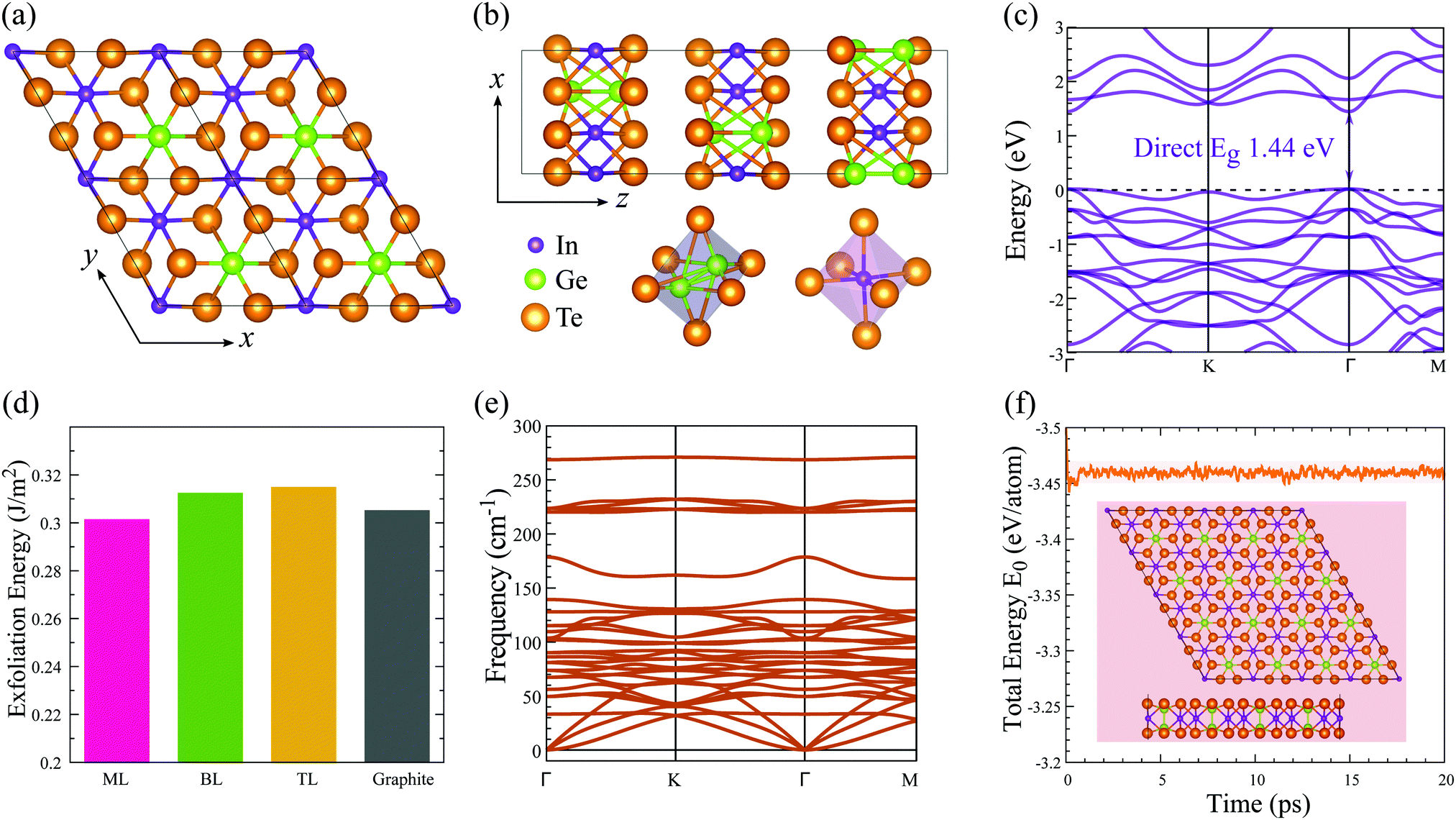 | ||
Fig. 1 Geometry of In2Ge2Te6 crystals: (a) top view of the 2 × 2 single-layer supercells and (b) side view of the bulk along the y axis as well as the octahedra. (c) Electronic band structure of the monolayer. The dashed line indicates the position of the Fermi energy set at 0 eV. (d) Calculated exfoliation energy of few-layer In2Ge2Te6 crystals in comparison with graphite. (e) Phonon dispersion curves and (f) AIMD evolution of the total energy for the monolayers. The insets show snapshots of single-layer structures after 10![[thin space (1/6-em)]](https://www.rsc.org/images/entities/char_2009.gif) 000 AIMD time-steps (color coding of atoms is the same as in (a and b)). 000 AIMD time-steps (color coding of atoms is the same as in (a and b)). | ||
| Crystal | a | vdW gap | E g |
|---|---|---|---|
| ML | 7.201 | — | 1.44 |
| BL-AA | 7.203 | 3.361 | 1.17 |
| BL-AB | 7.201 | 3.367 | 1.21 |
| TL | 7.204 | 3.310 | 1.12 |
| Bulk | 7.203, 21.485 | 3.315 | 0.91 |
| (7.086, 21.206) | (3.282) | — |
In contrast, quantum confinement has a large impact on the layer-dependent electronic bandgaps of In2Ge2Te6. Interestingly, the bulk crystal is an indirect bandgap semiconductor (Fig. S1, ESI†), while the monolayer has a direct bandgap (Fig. 1(c)). With a decrease of layer number, the bandgap changes from 0.91 eV (indirect) for the bulk to 1.44 eV (direct) for the monolayer (Table 1), which is an increase of 58%, significantly larger than in MoS2 (47%; 1.90 eV for the bulk and 1.29 eV for its monolayer).23 Not knowing the physical mechanism for the basis of the charge mobility, we estimated the mobility from deformation-potential theory, hence without accounting for scattering events with defects or the formation of small polarons. Interestingly, the carrier mobilities (Table 2) are also greatly affected by the numbers of layers. The largest carrier mobility of the monolayer is predicted to be ∼98 cm2 V−1 s−1 along the [010] direction, which is larger than the most-studied MoS2 monolayer (21 cm2 V−1 s−1 from Monte Carlo and DFT simulations),47 and it is enhanced up to 486 cm2 V−1 s−1 for the AB-stacked bilayer crystal and 4075 cm2 V−1 s−1 for the bulk phase (Table 2), confirming the presence of evident quantum-confinement effects. However, the carrier mobility of few-layer In2Ge2Te6 is not as large as graphene and black phosphorus (≥104 cm2 V−1 s−1), which might limit their application in high-speed field-effect transistors. On the other hand, few-layer and bulk crystals have comparable carrier mobilities to Si and GaAs (≥103 cm2 V−1 s−1) and relatively larger bandgaps than graphene, which is indicative of potential applications in optoelectronic devices and will be discussed later.
| Layer | Carrier | E DP | C | m* | μ |
|---|---|---|---|---|---|
| ML | e [100] | 5.549 | 38.370 | 0.692 | 36.9 |
| h [100] | 3.549 | 38.370 | 1.644 | 16.0 | |
| e [010] | 8.261 | 38.910 | 0.287 | 98.3 | |
| h [010] | 6.261 | 38.910 | 0.696 | 29.1 | |
| BL-AA | e [100] | 5.302 | 62.624 | 0.658 | 73.1 |
| h [100] | 3.052 | 62.624 | 1.541 | 40.2 | |
| e [010] | 9.333 | 63.863 | 0.313 | 106.3 | |
| h [010] | 7.583 | 63.863 | 0.672 | 34.9 | |
| BL-AB | e [100] | 4.852 | 62.027 | 0.481 | 161.7 |
| h [100] | 3.352 | 62.027 | 3.744 | 5.6 | |
| e [010] | 5.008 | 63.098 | 0.271 | 486.4 | |
| h [010] | 3.758 | 63.098 | 0.734 | 117.8 | |
| Bulk | e [100] | 9.537 | 196.129 | 0.104 | 2830.7 |
| h [100] | 5.710 | 196.129 | 0.945 | 95.6 | |
| e [010] | 9.096 | 251.913 | 0.103 | 4074.9 | |
| h [010] | 4.411 | 251.913 | 0.619 | 479.7 | |
Feasibility of experimental preparation
2D crystals often can be prepared by mechanical cleavage and liquid exfoliation from their layered bulk vdW-bonded crystals.10,48,49 The exfoliation energy of 2D In2Ge2Te6 was estimated by simulating the cleavage process (Fig. S2, ESI†). As shown in Fig. 1(d), our predicted exfoliation energy of the benchmark material graphite is ∼0.31 J m−2, which is in excellent agreement with the experimentally measured value (0.32 ± 0.03 J m−2)50 and previous theoretically calculated data (0.32 J m−2),51 ensuring the reliability and accuracy of our calculations. For 2D monolayer, bilayer and trilayer In2Ge2Te6, the exfoliation energies are predicted to be around 0.30 J m−2, very close to that of graphene, As2S3 (0.28 J m−2)52 and CrOCl (0.21 J m−2).27 As the previously predicted As2S3 and CrOCl monolayers have been successfully fabricated in recent experiments,53,54 we therefore anticipate that the mono- and few-layer In2Ge2Te6 should be able to be feasibly prepared in air from the bulk crystals by mechanical cleavage or similar preparation methods. Thanks to the weak vdW interactions between the adjacent layers, these 2D crystals are also potential candidates for the construction of vdW heterostructures or composites in future nanoelectronic applications.55,56Crystal stability
Lattice-dynamical calculations and molecular-dynamics simulations have been performed to assess the structural stability of 2D In2Ge2Te6 monolayers. According to the phonon-dispersion curves in Fig. 1(e), there are no imaginary phonon frequencies, indicating that single-layer In2Ge2Te6 is dynamically stable. The highest frequency of optical modes in the monolayer is around 270 cm−1, which is in fact indicative of weak chemical bonding.57,58Ab initio molecular-dynamics (AIMD) simulations at 300 K suggest that the monolayer is thermally stable, because the lattice structures are well maintained after 20 ps run times, as demonstrated by the AIMD snapshots (Fig. 1(f)). The appreciable thermal stability is further confirmed by the time-dependent total energies of the system, which only show small oscillations within 20 ps. During the AIMD simulations, all ions in the lattice vibrate around the local minima and no phase transition or separation was observed, demonstrating that 2D In2Ge2Te6 crystals should be highly stable at 300 K.Quantum-phase transitions
The electronic structures (Fig. 1(c)) of 2D In2Ge2Te6 monolayer show relatively flat valence bands below the Fermi energy, resulting in a very sharp peak in the density of states. This interesting characteristic is called a one-dimensional-like van Hove singularity and usually indicates electronic instability and thus controllable quantum-phase transitions, as reported in 2D GaSe, InP3 and nanoribbons.32,59,60Fig. 2(a) illustrates the calculated phase diagram of an electrostatically doped 2D In2Ge2Te6 monolayer at various carrier concentrations. Interestingly, the electronic instability can be driven by exchange interactions from both hole and electron doping. The hole-doped monolayer (Table S1 and Fig. S3, ESI†) turns out to have nonmagnetic and then ferromagnetic metallic states (3.43 × 1014 cm−2), which has been similarly observed in hole-doped GaSe and InP3 monolayers.32,59 Under electron doping, the In2Ge2Te6 monolayer first behaves as a nonmagnetic (NM) metal and then shows ferromagnetic (FM) metallicity when the carrier density is between 1.08 × 10¹⁴ and 2.12 × 1014 cm−2. A further increase of electron-doping density (>2.12 × 1014 cm−2) could induce an unusual magnetic transition from FM to antiferromagnetic (AFM) metallic states, which has rarely been reported before. These quantum-phase transitions could be achieved experimentally by applying electrolyte gates, with proven high carrier densities of up to 4 × 1014 cm−2 for both electrons and holes,61 or even by alloying the samples with higher valence elements, such as Ge/Sn at In sites and Sb/Bi at Ge sites. Besides the exotic semiconductor-to-metal transitions, 2D In2Ge2Te6 monolayer also presents electrically tunable magnetism, which is a different type of magnetic behavior compared with Cr2Ge2Te624,62 and renders it a very promising candidate for fundamental research on electromagnetic phenomena and for potential applications in spintronic devices.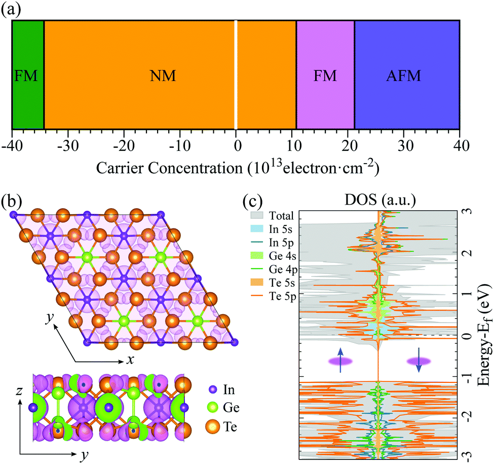 | ||
| Fig. 2 (a) Diagram of quantum-phase transitions in 2D In2Ge2Te6 monolayer under electrostatic doping, where negative and positive carrier concentrations correspond to hole and electron doping, respectively. (NM = non-magnetic; FM = ferromagnetic; AFM = anti-ferromagnetic.) The shaded-white region at zero indicates the semiconducting state of the pristine system. (b) Isosurfaces of spin charge-density differences (purple shading) along the z and x axes and (c) spin-dependent density of states (DOS) of the 2 × 2 monolayer supercell at an electron-doped concentration of 1.6 × 1014 cm−2. The Fermi level is set at 0 eV. | ||
To gain further insight on the quantum-phase transitions, the spin charge-density difference and density of states of a single-layer 2D crystal at an electron-doped concentration of 1.6 × 1014 cm−2 are illustrated in Fig. 2(b) and (c), respectively. It is clear that the magnetic states are dominated by the valence electrons from the indium and tellurium atoms, as indicated by the surrounding spin charge densities. This is consistently demonstrated by the spin-dependent projected density of states shown in Fig. 2(c), where the electronic states around the Fermi level are primarily contributed by the 5 s orbital of the In atoms and 5 p orbital of the Te atoms in both majority and minority spin channels. Below the Fermi energy, it is mostly determined by the Te-5 p orbitals. A similar phenomenon can be observed in the DOS of 2D monolayer crystals at different doping concentrations (Fig. S4, ESI†). Therefore, it would be very interesting to further tune the properties of 2D In2Ge2Te6 by Te defect engineering.
Atomic stacking under vdW pressure
The influence of vdW pressure can induce novel physical phenomena in nano-enclosures and create new chemical compounds.46 To tune the vdW interactions of layered In2Ge2Te6, here we constructed AA- and AB-stacked bilayers, as depicted in Fig. 3(a). Different amplitudes of vdW pressures are applied vertically along the vdW directions of the bilayer crystals, which could be experimentally achieved with a scanning tunnelling microscope tip63 or by fabricating the samples encapsulated between the flakes of boron nitride or few-layer graphite,40,45 where the deformation could be controlled via the distance between two flakes. Fig. 3(b) presents the evolution of the relative total energy (EAA − EAB) with pressure and change of vdW gaps. Obviously, under zero pressure and for all tensile pressures, the free-standing AB-stacked bilayer is always the ground state as its total energy is lower than that of the AA-stacked one. With an increase of compressive pressure (corresponding to a decrease of the vdW gap), the relative total energy becomes zero at 1.56 GPa (that is a reduction of the interlayer distance of 0.62 Å), indicating there is a possible stacking transition from the AB to AA configurations, which may due to steric effects as there is no newly formed chemical bond between adjacent layers. Our lattice-dynamical simulation further demonstrates that the AA-stacked bilayer is stable at 1.56 GPa, because no imaginary mode is found in the calculated phonon-dispersion curves (Fig. 3(c)).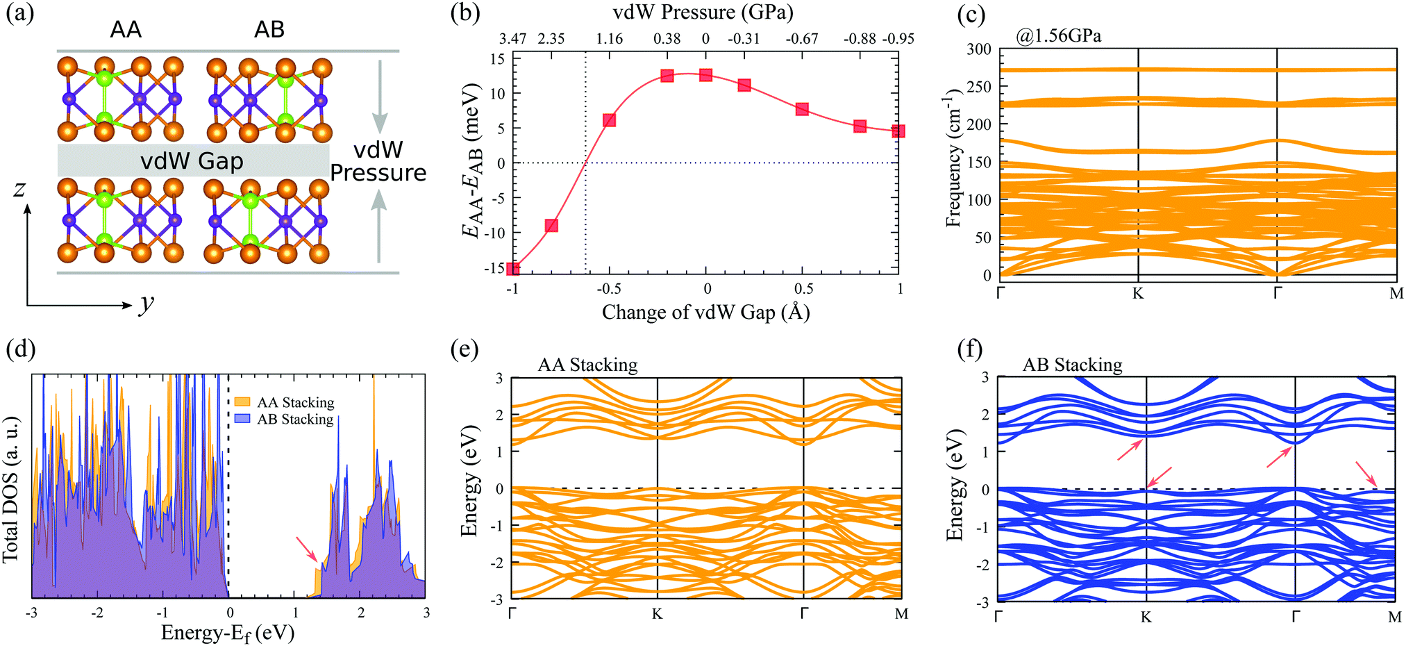 | ||
| Fig. 3 (a) Schematic diagram of AA- and AB-stacked bilayers under vdW pressure. (b) Relative total energy of the bilayer systems with respect to vdW pressure and gap change. The dotted lines indicate the zero-energy point and transition pressure. (c) Phonon-dispersion curves of an AA-stacked bilayer under 1.56 GPa vdW pressure. (d) Total electronic density of states as well as electronic band structures of (e) AA- and (f) AB-stacked bilayers under zero pressure. The Fermi energy is denoted by a horizontal dashed line and set to 0 eV. The red arrows indicate obvious differences of bands at the top of the valence band and bottom of the conduction band. | ||
In addition, the electronic structures of these AA- and AB-stacked bilayers are different, as shown in Fig. 3(d), which would be helpful for experimentalists to characterize these stacking configurations. The calculated electronic density of states suggests that the valence bands of both AA- and AB-stacked bilayers are very similar and the most significant difference is observed in their conduction bands. The conduction-band minimum in the AA-stacked bilayer is lower in energy than that in the AB-stacked one, which leads to a ∼40 meV smaller electronic bandgap of the former, indicating their different electronic properties. Further evidence could be found in the electronic band structures (Fig. 3(e and f)). The AB-stacked bilayer shares some band features with the monolayer, e.g., dispersive bands at the top of the valence band and at the bottom of the conduction band, while the AA-stacked bilayer has relatively flat bands, especially around the conduction-band minimum. As a result, the AB-stacked bilayer shows much higher overall carrier mobilities compared with the AA-stacked crystal (Table 2). It is noticed that, for both stackings under compressive vdW pressure, the lowest conduction bands around Γ point move down toward the Fermi energy and the electronic bandgap decreases, while the top valence bands do not change obviously (Table S2 and Fig. S5, ESI†). Therefore, the electronic and stacking properties of AA- and AB-stacked bilayers could be possibly tuned via vdW pressure and electrically detected by experiments, indicating potential utilization in nanoelectronic sensors.45
Optical absorption and photovoltaic conversion
As discussed above, the In2Ge2Te6 monolayer has a direct bandgap of 1.44 eV, which is very close to that of GaAs, suggesting its great potential for optoelectronic and photovoltaic applications. To assess the optical performance, we predicted the absorption coefficients of the monolayer, bilayer, and trilayer forms of In2Ge2Te6 in comparison with the absorption spectra of GaAs and Si crystals. As illustrated in Fig. 4(a), we notice that the calculated absorption spectra of GaAs and Si are in reasonable agreement with experimental measurements,64–66 where the small discrepancies between theory and experiment can be understood as being due to the surface roughness of crystal samples and temperature effects, which are not included in our calculations. It is interesting to see that the overall in-plane absorption coefficients of the single-layer In2Ge2Te6 crystal are appreciably large (∼105 cm−1) and comparable to that of GaAs, while being significantly larger than that of intrinsic silicon.65 Especially, all of the 2D In2Ge2Te6 crystals exhibit a much stronger absorbance than GaAs in the wavelength range of 520–700 nm (Fig. 4(a)). We also noticed that the AA- and AB-stacked bilayers show a similar optical absorbance, indicating that the stacking configuration does not have a great impact on the absorption performance. Thanks to the extraordinary visible-light absorbance, these 2D crystals offer great possibilities for atomically-thin optoelectronic devices, as further discussed below.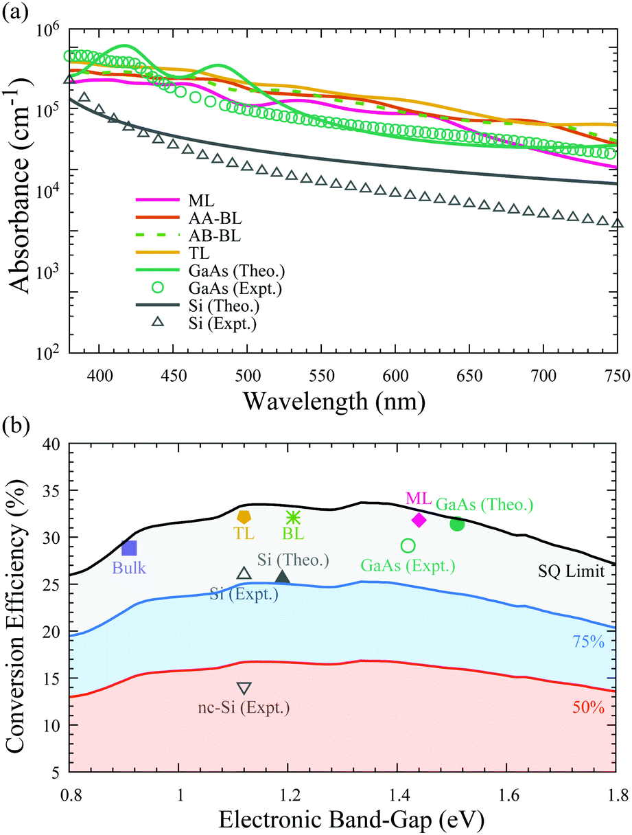 | ||
| Fig. 4 (a) Calculated optical-absorption spectrum of 2D In2Ge2Te6 from the time-dependent Hartree–Fock method compared with GaAs64 and silicon65,66 crystals in the visible-light wavelength range (380–750 nm). (b) Theoretical (Theo.) photovoltaic conversion efficiency of monolayer (ML), AB-stacked bilayer (BL), ABC-stacked trilayer (TL) and bulk In2Ge2Te6 crystals in AM1.5G sunlight, as well as experimental (Expt.) data for GaAs and silicon.6 The shaded regions indicate 50%, 75% and 100% of the Shockley–Queisser (SQ) limit.67 | ||
Based on the Shockley–Queisser (SQ) theory,67,68 the conversion efficiency (spectroscopic-limited maximum efficiency, SLME) can be calculated using the absorption coefficients to describe the photovoltaic performance of a solar cell, assuming that the material is free of exciton, Holstein-like polaron and defect effects. The predicted photovoltaic conversion efficiencies under the standard AM1.5G solar spectrum69 are summarized in Fig. 4(b) for thin-film solar cells with a typical thickness of ∼2 μm;70 nevertheless, such an assumption should be rigorously checked by future experiments. Taking the most efficient single-junction GaAs solar cell as a benchmark, its conversion efficiency is calculated to be 31.4%, which is in excellent agreement with previous simulation results (32%)71 and slightly higher than the experimental world-record value (29.1%),6 suggesting good reliability of our theoretical estimation. Strikingly, the predicted conversion efficiency of the single-layer In2Ge2Te6 crystal is 31.8%, which is comparable to that of GaAs. The efficiencies of bilayer (32.1%) and trilayer (32.2%) In2Ge2Te6 crystals are even higher than GaAs and 2D trilayer silicene (29%),71 while the bulk material shows an efficiency of 28.8%, close to the SQ limit, indicating their great potential for photovoltaic and optoelectronic applications. As 2D In2Ge2Te6 may exhibit a large absorption in the infra-red region, which could lead to extensive heating during operation and possible degradation, therefore careful attention should be paid to the design of high-temperature optoelectronic devices.
As indicated by the SQ limit, the electronic bandgap has a large effect on the photovoltaic conversion efficiency. Fig. 5(a) illustrates the bandgaps of the single-layer orthogonal cell of In2Ge2Te6 under uniaxial and biaxial strains. Apparently, the bandgap could be well tuned from ∼1.0 to 1.5 eV by applying strains and it varies gradually, but not monotonically like phosphorene and many other 2D materials under compressive and tensile loadings.49 This interesting behaviour is due to the aforementioned one-dimensional-like van Hove singularities (almost flat valence bands) which also result in a nonmonotonic shift of the VBM under various strains (Fig. S6, ESI†). The response of the SLME conversion efficiency of biaxially strained monolayer In2Ge2Te6 coupling with various bandgaps is summarized in Fig. 5(b). Very large SLMEs can be achieved at around 1.32–1.42 eV under appropriate strains. It seems that the bandgap plays a more important role than the optical absorbance in improving the conversion efficiency of strained crystals, where the absorption spectra vary slightly under strain and are still comparable to that of GaAs (Fig. S7, ESI†). As the SLME changes obviously with bandgap (Fig. 5(b) and Fig. S8, ESI†), it is possible to introduce external electrical/magnetic fields72,73 to optimize the bandgap and hence improve the photovoltaic performance of these 2D crystals.
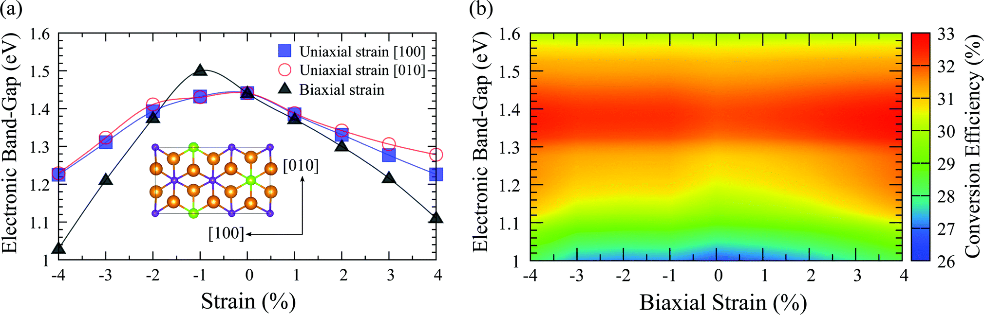 | ||
| Fig. 5 Calculated (a) electronic bandgap of the In2Ge2Te6 monolayer under various strains and (b) photovoltaic conversion efficiency of biaxially strained single-layer In2Ge2Te6 crystal, using the HSE06 functional. | ||
To summarize, we have predicted new 2D In2Ge2Te6 semiconductors with excellent electronic and optical properties from ab initio simulations. These 2D crystals have direct bandgaps (from 1.12 to 1.44 eV), possess moderate carrier mobilities (up to ∼486 cm2 V−1 s−1) and indicate excellent dynamical and thermal stability, which are very appealing for future microelectronic and optoelectronic applications. They show a low exfoliation energy (∼0.30 J m−2) and hence it is expected that they could be experimentally fabricated by mechanical cleavage. Of the most interest, all of them are predicted to exhibit extraordinary light absorption in the entire visible solar spectrum and a high photovoltaic conversion efficiency (≥31.8%), which is comparable to the most efficient single-junction GaAs solar cell (31.4%) and trilayer silicene (29%). Therefore, these novel 2D crystals will be of great promise for next-generation nanoelectronics.
In addition, two types of phase transformations have been found in the proposed 2D In2Ge2Te6 crystals. We highlighted that unusual quantum-phase transitions from a semiconductor to a FM/AFM-metallic state could be achieved in single-layer In2Ge2Te6 by electrostatic carrier doping, and these transitions are dominated by the In-5 s and Te-5 p orbitals. Using the In2Ge2Te6 bilayer as a prototypical system, we further revealed a possible AB to AA stacking transition at 1.56 GPa and explored the electronic structures under vdW pressure, demonstrating that the application of vdW pressure is an effective and convenient strategy to manipulate the electronic and stacking properties of ultrathin 2D crystals. Taken together, our work will stimulate fundamental investigations on quantum phase transitions and potential applications of high-performance 2D IIIA–VIA semiconductors for future spintronic and optoelectronic devices.
Conflicts of interest
There are no conflicts to declare.Acknowledgements
This work is supported by the National Key Research and Development Program of China (2017YFB0701700) and the National Natural Science Foundation of China (61874146, 21803005 and 51872017).References
- C. H. Ahn, J.-M. Triscone and J. Mannhart, Nature, 2003, 424, 1015–1018 CrossRef CAS.
- K. Kim, J.-Y. Choi, T. Kim, S.-H. Cho and H.-J. Chung, Nature, 2011, 479, 338 CrossRef CAS.
- K. Kang, S. Xie, L. Huang, Y. Han, P. Y. Huang, K. F. Mak, C.-J. Kim, D. Muller and J. Park, Nature, 2015, 520, 656 CrossRef CAS.
- S. Moss and A. Ledwith, Chemistry of the Semiconductor Industry, Springer, 1989 Search PubMed.
- D. Fisher and I. Bahl, Gallium Arsenide IC Applications Handbook, Elsevier, 1995 Search PubMed.
- NREL, Research Cell Record Efficiency Chart, 2019, https://www.nrel.gov/pv/assets/pdfs/pv-efficiency-chart.20190103.pdf.
- J. M. Kikkawa and D. D. Awschalom, Nature, 1999, 397, 139–141 CrossRef CAS.
- S. A. Wolf, D. D. Awschalom, R. A. Buhrman, J. M. Daughton, M. S. Von, M. L. Roukes, A. Y. Chtchelkanova and D. M. Treger, Science, 2001, 294, 1488 CrossRef CAS.
- M. A. Olshavsky, A. N. Goldstein and A. P. Alivisatos, J. Am. Chem. Soc., 1990, 112, 9438–9439 CrossRef CAS.
- K. S. Novoselov, A. K. Geim, S. Morozov, D. Jiang, Y. Zhang, S. Dubonos, I. Grigorieva and A. Firsov, Science, 2004, 306, 666–669 CrossRef CAS.
- A. K. Geim and K. S. Novoselov, Nat. Mater., 2007, 6, 183–191 CrossRef CAS.
- X. Duan, C. Wang, J. C. Shaw, R. Cheng, Y. Chen, H. Li, X. Wu, Y. Tang, Q. Zhang and A. Pan, et al. , Nat. Nanotechnol., 2014, 9, 1024 CrossRef CAS.
- S. Zhang, Z. Yan, Y. Li, Z. Chen and H. Zeng, Angew. Chem., Int. Ed., 2015, 54, 3112–3115 CrossRef CAS.
- J. Dai and X. C. Zeng, Angew. Chem., 2015, 127, 7682–7686 CrossRef.
- J. Zhao, H. Liu, Z. Yu, R. Quhe, S. Zhou, Y. Wang, C. C. Liu, H. Zhong, N. Han, J. Lu, Y. Yao and K. Wu, Prog. Mater. Sci., 2016, 83, 24–151 CrossRef CAS.
- H. Zhang, Y. Li, J. Hou, K. Tu and Z. Chen, J. Am. Chem. Soc., 2016, 138, 5644–5651 CrossRef CAS.
- M. Chhowalla, D. Jena and H. Zhang, Nat. Rev. Mater., 2016, 1, 16052 CrossRef CAS.
- Q. Li, Q. Zhou, X. Niu, Y. Zhao, Q. Chen and J. Wang, J. Phys. Chem. Lett., 2016, 7, 4540–4546 CrossRef CAS.
- C. Tan, X. Cao, X.-J. Wu, Q. He, J. Yang, X. Zhang, J. Chen, W. Zhao, S. Han, G.-H. Nam, M. Sindoro and H. Zhang, Chem. Rev., 2017, 117, 6225–6331 CrossRef CAS.
- B. Huang, G. Clark, E. Navarro-Moratalla, D. R. Klein, R. Cheng, K. L. Seyler, D. Zhong, E. Schmidgall, M. A. Mcguire and D. H. Cobden, Nature, 2017, 546, 270 CrossRef CAS.
- N. Lu, Z. Zhuo, H. Guo, P. Wu, W. Fa, X. Wu and X. C. Zeng, J. Phys. Chem. Lett., 2018, 9, 1728–1733 CrossRef CAS.
- D. R. Klein, D. MacNeill, J. L. Lado, D. Soriano, E. Navarro-Moratalla, K. Watanabe, T. Taniguchi, S. Manni, P. Canfield, J. Fernández-Rossier and P. Jarillo-Herrero, Science, 2018, 360, 1218–1222 CrossRef CAS.
- K. F. Mak, C. Lee, J. Hone, J. Shan and T. F. Heinz, Phys. Rev. Lett., 2010, 105, 136805 CrossRef.
- C. Gong, L. Li, Z. Li, H. Ji, A. Stern, Y. Xia, T. Cao, W. Bao, C. Wang and Y. Wang, Nature, 2017, 546, 265 CrossRef CAS.
- Z. Hao, H. Li, S. Zhang, X. Li, G. Lin, X. Luo, Y. Sun, Z. Liu and Y. Wang, Sci. Bull., 2018, 63, 825–830 CrossRef CAS.
- R. Lefèvre, D. Berthebaud, O. Lebedev, O. Pérez, C. Castro, S. Gascoin, D. Chateigner and F. Gascoin, J. Mater. Chem. A, 2017, 5, 19406–19415 RSC.
- N. Miao, B. Xu, L. Zhu, J. Zhou and Z. Sun, J. Am. Chem. Soc., 2018, 140, 2417–2420 CrossRef CAS.
- C. Huang, J. Feng, F. Wu, D. Ahmed, B. Huang, H. Xiang, K. Deng and E. Kan, J. Am. Chem. Soc., 2018, 140, 11519–11525 CrossRef CAS.
- N. Lu, Z. Zhuo, Y. Wang, H. Guo, W. Fa, X. Wu and X. C. Zeng, J. Phys. Chem. Lett., 2018, 9, 6568–6575 CrossRef CAS.
- J. Jiao, N. Miao, Z. Li, Y. Gan, J. Zhou and Z. Sun, J. Phys. Chem. Lett., 2019, 10, 3922–3928 CrossRef CAS.
- X. Li, X. Wu and J. Yang, J. Am. Chem. Soc., 2014, 136, 11065–11069 CrossRef CAS.
- N. Miao, B. Xu, N. C. Bristowe, J. Zhou and Z. Sun, J. Am. Chem. Soc., 2017, 139, 11125–11131 CrossRef CAS.
- Y. Zhao, L. Lin, Q. Zhou, Y. Li, S. Yuan, Q. Chen, S. Dong and J. Wang, Nano Lett., 2018, 18, 2943–2949 CrossRef CAS.
- Q. Wu, W. W. Xu, B. Qu, L. Ma, X. Niu, J. Wang and X. C. Zeng, Mater. Horiz., 2017, 4, 1085–1091 RSC.
- X. Zhang, B. Wang, X. Niu, Y. Li, Y. Chen and J. Wang, Mater. Horiz., 2018, 5, 1058–1064 RSC.
- S. Wu, J. S. Ross, G.-B. Liu, G. Aivazian, A. Jones, Z. Fei, W. Zhu, D. Xiao, W. Yao and D. Cobden, et al. , Nat. Phys., 2013, 9, 149 Search PubMed.
- K. Liu, L. Zhang, T. Cao, C. Jin, D. Qiu, Q. Zhou, A. Zettl, P. Yang, S. G. Louie and F. Wang, Nat. Commun., 2014, 5, 4966 Search PubMed.
- Y. Cao, V. Fatemi, S. Fang, K. Watanabe, T. Taniguchi, E. Kaxiras and P. Jarillo-Herrero, Nature, 2018, 556, 43 CrossRef CAS.
- Y. Zhao, J.-J. Zhang, S. Yuan and Z. Chen, Adv. Funct. Mater., 2019, 29, 1901420 CrossRef.
- M. Yankowitz, S. Chen, H. Polshyn, Y. Zhang, K. Watanabe, T. Taniguchi, D. Graf, A. F. Young and C. R. Dean, Science, 2019, 363, 1059–1064 CrossRef CAS.
- Y. Cao, V. Fatemi, A. Demir, S. Fang, S. L. Tomarken, J. Y. Luo, J. D. Sanchez-Yamagishi, K. Watanabe, T. Taniguchi and E. Kaxiras, et al. , Nature, 2018, 556, 80 CrossRef CAS.
- Y. Xie, B. Lian, B. Jäck, X. Liu, C.-L. Chiu, K. Watanabe, T. Taniguchi, B. A. Bernevig and A. Yazdani, Nature, 2019, 572, 101–105 CrossRef CAS.
- A. Kerelsky, L. J. McGilly, D. M. Kennes, L. Xian, M. Yankowitz, S. Chen, K. Watanabe, T. Taniguchi, J. Hone, C. Dean, A. Rubio and A. N. Pasupathy, Nature, 2019, 572, 95–100 CrossRef CAS.
- Y. Jiang, X. Lai, K. Watanabe, T. Taniguchi, K. Haule, J. Mao and E. Y. Andrei, Nature, 2019, 573, 91–95 CrossRef CAS.
- M. Yankowitz, J. Jung, E. Laksono, N. Leconte, B. L. Chittari, K. Watanabe, T. Taniguchi, S. Adam, D. Graf and C. R. Dean, Nature, 2018, 557, 404 CrossRef CAS.
- K. S. Vasu, E. Prestat, J. Abraham, J. Dix, R. J. Kashtiban, J. Beheshtian, J. Sloan, P. Carbone, M. Neek-Amal, S. J. Haigh, A. K. Geim and R. R. Nair, Nat. Commun., 2016, 7, 12168 CrossRef CAS.
- G. Gaddemane, W. G. Vandenberghe, M. L. V. de Put, S. Chen, S. Tiwari, E. Chen and M. V. Fischetti, Phys. Rev. B, 2018, 98, 115416 CrossRef CAS.
- K. S. Novoselov, D. Jiang, F. Schedin, T. J. Booth, V. V. Khotkevich, S. V. Morozov and A. K. Geim, Proc. Natl. Acad. Sci. U. S. A., 2005, 102, 10451–10453 CrossRef CAS.
- H. Liu, A. T. Neal, Z. Zhu, Z. Luo, X. Xu, D. Tománek and P. D. Ye, ACS Nano, 2014, 8, 4033–4041 CrossRef CAS.
- R. Zacharia, H. Ulbricht and T. Hertel, Phys. Rev. B: Condens. Matter Mater. Phys., 2004, 69, 155406 CrossRef.
- E. Ziambaras, J. Kleis, E. Schröder and P. Hyldgaard, Phys. Rev. B: Condens. Matter Mater. Phys., 2007, 76, 155425 CrossRef.
- N. Miao, J. Zhou, B. Sa, B. Xu and Z. Sun, J. Alloys Compd., 2017, 699, 554–560 CrossRef CAS.
- M. Šiškins, M. Lee, F. Alijani, M. R. van Blankenstein, D. Davidovikj, H. S. J. van der Zant and P. G. Steeneken, ACS Nano, 2019, 13, 10845–10851 CrossRef.
- T. Zhang, Y. Wang, H. Li, F. Zhong, J. Shi, M. Wu, Z. Sun, W. Shen, B. Wei, W. Hu, X. Liu, L. Huang, C. Hu, Z. Wang, C. Jiang, S. Yang, Q. Zhang and Z. Qu, ACS Nano, 2019, 13, 11353–11362 CrossRef CAS.
- B. Sa, J. Zhou, Z. Sun, J. Tominaga and R. Ahuja, Phys. Rev. Lett., 2012, 109, 096802 CrossRef.
- C. Tan and H. Zhang, J. Am. Chem. Soc., 2015, 137, 12162–12174 CrossRef CAS.
- B. Jiang, P. Qiu, E. Eikeland, H. Chen, Q. Song, D. Ren, T. Zhang, J. Yang, B. B. Iversen, X. Shi and L. Chen, J. Mater. Chem. C, 2017, 5, 943–952 RSC.
- S. Acharya and A. Soni, AIP Conf. Proc., 2019, 2115, 030624 CrossRef.
- T. Cao, Z. Li and S. G. Louie, Phys. Rev. Lett., 2015, 114, 236602 CrossRef.
- Y.-W. Son, M. L. Cohen and S. G. Louie, Nature, 2006, 444, 347–349 CrossRef CAS.
- D. K. Efetov and P. Kim, Phys. Rev. Lett., 2010, 105, 256805 CrossRef.
- Y. Sun, R. C. Xiao, G. T. Lin, R. R. Zhang, L. S. Ling, Z. W. Ma, X. Luo, W. J. Lu, Y. P. Sun and Z. G. Sheng, Appl. Phys. Lett., 2018, 112, 072409 CrossRef.
- M. Yankowitz, K. Watanabe, T. Taniguchi, P. San-Jose and B. J. LeRoy, Nat. Commun., 2016, 7, 13168 CrossRef CAS.
- S. Adachi, Optical Constants of Crystalline and Amorphous Semiconductors, Springer, US, 1999 Search PubMed.
- M. A. Green and M. J. Keevers, Prog. Photovolt: Res. Appl., 1995, 3, 189–192 CrossRef CAS.
- D. E. Aspnes and A. A. Studna, Phys. Rev. B: Condens. Matter Mater. Phys., 1983, 27, 985–1009 CrossRef CAS.
- W. Shockley and H. J. Queisser, J. Appl. Phys., 1961, 32, 510–519 CrossRef CAS.
- L. Yu and A. Zunger, Phys. Rev. Lett., 2012, 108, 068701 CrossRef.
- A. G173-03, Standard Tables for Reference Solar Spectral Irradiances, 2012, DOI: 10.1520/G0173-03R12.
- G. Bauhuis, P. Mulder, E. Haverkamp, J. Huijben and J. Schermer, Sol. Energy Mater. Sol. Cells, 2009, 93, 1488–1491 CrossRef CAS.
- J. Lv, M. Xu, S. Lin, X. Shao, X. Zhang, Y. Liu, Y. Wang, Z. Chen and Y. Ma, Nano Energy, 2018, 51, 489–495 CrossRef CAS.
- W. Zhang, Y. Xu, H. Wang, C. Xu and S. Yang, Sol. Energy Mater. Sol. Cells, 2011, 95, 2880–2885 CrossRef CAS.
- Y. Wang, Z. Xia, L. Liu, W. Xu, Z. Yuan, Y. Zhang, H. Sirringhaus, Y. Lifshitz, S.-T. Lee, Q. Bao and B. Sun, Adv. Mater., 2017, 29, 1606370 CrossRef.
Footnote |
| † Electronic supplementary information (ESI) available: Computational methodologies. Tables and figures for the structural, magnetic, optical properties, phonon dispersions and electronic structures. See DOI: 10.1039/d0nh00395f |
| This journal is © The Royal Society of Chemistry 2020 |