DOI:
10.1039/D0NH00319K
(Communication)
Nanoscale Horiz., 2020,
5, 1487-1495
Polarization-dependent asymmetric transmission using a bifacial metasurface†
Received
25th May 2020
, Accepted 4th September 2020
First published on 7th September 2020
Abstract
One of the most important research topic in optics and photonics is the design of metasurfaces to substitute conventional optical elements that demonstrate unprecedented merits in terms of performance and form factor. In this context, full-space control of metasurfaces that makes it possible to manipulate scattered light in transmission and reflection spaces simultaneously, is proposed as the next-generation scheme in optics, with a potential for applications such as 360° holographic images and novel optical systems. However, previously designed metasurfaces lacked functionality because the desired operation occurs under preconditioned light; therefore, they are difficult to use in real applications. Here, we present a design method that enables polarization-dependent full-space control, in which two independent and arbitrary phase profiles can be addressed to each space. Upon introducing a phase gradient value to realize the critical angle condition, conversion of transmissive into reflective operation is realized. Then, rectangular nanopillars are utilized to facilitate polarization beam splitting with the desired phase. Three samples were fabricated and measured based on the proposed scheme.
New concepts
Here, we report a novel bifacial metasurface platform that can send different phase shift values into transmission and reflection spaces altered by polarization states. We utilized the designed phase gradient to flip the transmissive operation into reflection, which becomes possible using the specific critical angle with normally incident conditions. Linearly birefringent nanopillars enable two independent phase values with an arbitrary polarization pair. Interleaving two nanopillars in a unit cell makes it possible to realize polarization-selective space control: in contrast to the conventional interleaved metasurface, where each meta-atom operates separately, the operation of a metasurface is determined by its gradient. This scheme can be applied to other metasurface designs as well. Because this work reinforces the ability of conventional metasurfaces to be applied in full-space modulation (i.e., both in the transmission direction and the reflection direction), the proposed scheme is expected to pave a way for the adoption of metasurfaces in future optic components, such as 360° vectorial holograms.
|
Introduction
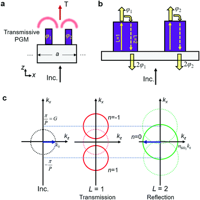
Metasurfaces, which are planar optical components engineered for specific optic or photonic operations, are promising candidates for future display applications, considering their ultra-small form factors and the unprecedented capacity to control their light properties.1–11 Among various abilities of metasurfaces, spatial light modulation at subwavelength resolution has been utilized to change the angular spectrum information of output light, in turn functioning as a compact holographic data storage system.12,13 Like crystals have anisotropic properties due to geometric asymmetry of their atomic structures, birefringent characteristics can be obtained by changing the size or shape of the unit structure, applied in both the far and near fields.14–17 Anisotropic nanopillars create differences in the phase retardation of the linear orthogonal polarization states; this approach doubles the information density of metasurfaces, which can then be used as multifunctional devices. In early studies, the holographic method was utilized to encode two different holograms.18 Also, spatial multiplexing of meta-atoms of various operations increases the information capacity and degrees of freedom of design, followed by extension of the functionality of the devices.19–23 Recently, using layered holographic color pixels that can control both the amplitude of the spectrum and phase retardation value, holographic color printing has been realized for full-field control and multiplexing.24 However, most multifunctional metasurfaces can affect either the transmission or reflection space, only to discard the remaining area; this restricts the freedom of designing optics systems with metasurfaces. Several studies have demonstrated full-space modulation by various techniques to overcome this issue; however, most of these systems operate in the gigahertz range and consist of cascaded metallic structures.25–27 Therefore, they are difficult to use in optical frequency applications, considering their fabrication difficulty and absorption loss issues. Some recent studies have suggested full-space modulation in the optical frequency regime with simply shaped meta-atoms.28,29 Especially, in our previous study, full-space phase modulation was realized using the generalized Kerker effect, controlling the portion of excited multipole modes that possess different phase parities with each space.28 In these studies, however, including our previous study, the metasurfaces lack polarization-dependent characteristics or operate with preconditioned incident light; therefore, it is difficult to utilize them in various applications.28–30
Another important branch of light control which becomes possible with metasurfaces is the implementation of a phase gradient. Indeed, phase gradient metasurfaces (PGMs) have been utilized in the past for acquisition of desired light beam trajectories by generalized Snell's law (GSL).3,31–33 This is because the light rays obtain an additional transverse wavevector from the phase gradient, which results in anomalous refraction or reflection.34 However, GSL is found to be insufficient to explain the light beam path, especially when light impinges with the critical angle condition. In this condition, the lattice vector of the periodic structure replaces the phase gradient; this reveals various interesting phenomena, such as high order diffraction, asymmetric transmission and retroreflection.35–38 However, while the inherited physics has been theoretically revealed in past studies, devices utilizing the relevant content is still rare.39,40 Because the current research framework of metasurfaces which modulate full space lacks polarization response, the combination of the phase gradient for asymmetric transmission and a conventional polarization multiplexing scheme may pave the way to achieve novel polarization-selective full-space control in the electromagnetic regime.14,15,35
In this article, a metasurface platform is proposed which achieves asymmetric transmission according to the polarization states of incident light and conveys two independent phase profiles to each space at the same time. We utilize a birefringent nanopillar as a unit to impart different phase profiles at two arbitrary orthogonal polarizations. Next, we show that the transmissive metasurface possessing a specific phase gradient can be utilized to reflection-type using the critical angle condition.35 As a result, control of the transmission and reflection can be realized by polarization of the incident light, and at the same time, their phases can be determined independently. The fabrication and measurements of the proposed scheme are also conducted with two examples (beam steering and holographic image generation) and verified with three different polarization pairs. Contrary to other implementations, here, the proposed scheme considers full-space modulation.1–9 We expect our metasurface design to be applied in a diversity of optical setups due to its compact but outstanding ability of light manipulation in full space, providing a new way to simplify existing systems. Moreover, as a holographic storage system, this scheme may open a new horizon for image encryption and decryption as well as for real 360° vectorial holograms.16,29
Results and discussion
Basic metasurface design
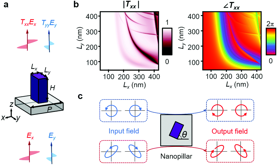
The basic framework of the proposed metasurface consists of amorphous silicon rectangular nanopillars on a quartz substrate, as shown in Fig. 1a. The material choice is attributed to its high index and low absorptivity at 980 nm wavelength (nSi,980 nm = 3.6 + 0.013i). The unit cell has a 450 nm pixel pitch (P in Fig. 1a), which was determined not to cause diffraction considering the refractive index of the substrate (SiO2, n = 1.44). Each nanopillar is 500 nm in height (H in Fig. 1a), which is about half the wavelength in free space (980 nm); they were optimized to have high transmittance (0.8–1) and sufficient birefringence at the same time. Finite element method simulations were performed using commercially available software (COMSOL Multiphysics). To avoid unphysical scattering and provide better agreement with the experimental results, the simulations considered pillars with rounded edges (Fig. S1, ESI†). The amplitude and phase of Txx and Tyy were obtained while varying the structural parameters Lx and Ly from 50 nm to 430 nm, as shown in Fig. 1b. From this computed result, one can find the nanopillar that minimizes the mean squared error, calculated as follows:| | | E = |Txx − ejϕ1|2 + |Tyy − ejϕ2|2 | (1) |
where ϕ1 and ϕ2 are the desired phase values. Using eqn (1), we obtained the structural information of the nanopillar which delivers the phases of ϕ1 and ϕ2 to x- and y-polarized light, respectively. For the detailed parameter set, see Fig. S2 in the ESI.† This phase shift disparity by incident polarization stems from the effective propagation length difference due to the shape of the nanopillar. This property endows the proposed platform with sensitivity to wavelength changes (see Fig. S3, ESI†).
 |
| | Fig. 1 Schematic and transmission coefficients of the nanopillar which is used as a unit structure throughout this article. (a) Schematic of the rectangular nanopillar expressed with structural parameters. The structure is illuminated from the bottom. The nanopillar is composed of amorphous silicon, structured on a quartz wafer. (b) Simulation results of the amplitude and phase of transmission Txx while varying Lx and Ly of a single nanopillar. (c) Conceptual schematic of the mechanism of phase modulation of an arbitrary polarization pair. When the nanopillar rotation is introduced, phase modulation at the arbitrary polarization pair is possible with flipped-handedness, as described in the text. | |
In addition, several previous studies revealed that this linearly birefringent metasurface platform can also impart two different phase shifts into other polarization pairs.14,15 This is possible by introducing the in-plane rotation angle to the nanopillar. For example, if circularly polarized light shines on the nanopillar, the cross-polarized component of the transmission is expressed as:
| | | Tcross = (Txx − Tyy)ej2σθ/2 | (2) |
where
σ is the parameter determined by the handedness of circular polarization of the incident light and
θ is the rotation angle of the nanopillar, as shown in
Fig. 1c.
15 Herein,
σ is +1 or −1 for right or left circular polarization, respectively. According to
eqn (2), the phase of
Tcross is dependent on the handedness of the polarization due to the part of e
j2σθ. As the amplitude and phase of (
Txx −
Tyy) are controllable by the dimensions of the nanopillar, the maximal value of
Tcross with two independent phase shift values by input circular polarization can be achieved. This is also achievable for the elliptical polarization pair. The derivation can be found in ESI,
† part 1, retrieved by Jones matrix calculation.
14,15 It is notable that unlike the conditions in which linearly polarized light is used, the component to which the phase is added is the handedness-flipped version of the incident light (see
Fig. 1c). As a result, for an arbitrary polarization pair, polarization multiplexed phase control is realized.
Phase gradient metasurface for reflective operation
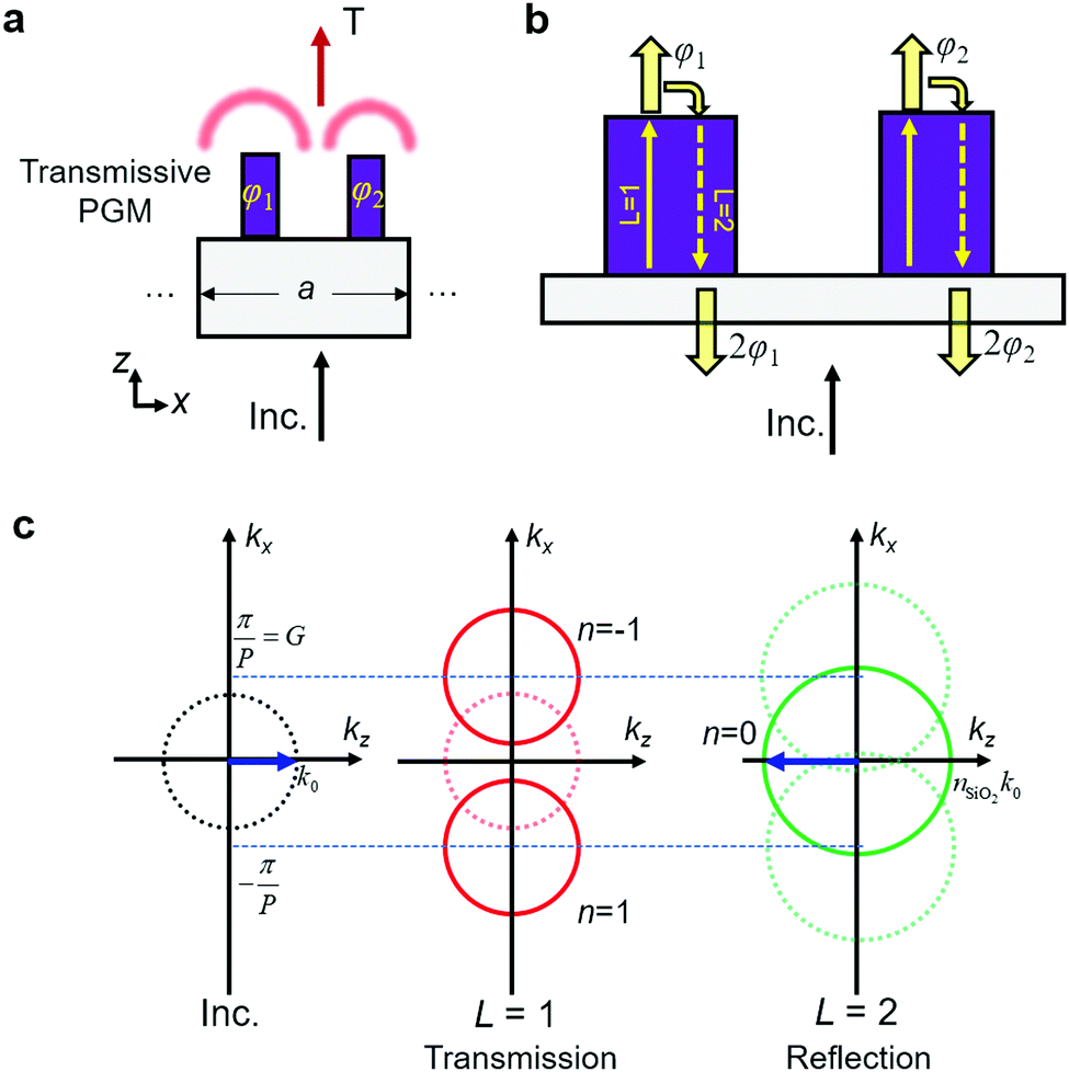
In this section, we provide a method which allows us to obtain induced reflection using PGMs.35,36 Our scheme can be explained by the integer parity design of two meta-atoms, assisted by the diffraction law of parity reversal and the critical angle condition, to demonstrate the reflective operation from a transmissive-type device.35 Suppose that a transmissive PGM of periodicity a is designed with gradual phase shift values from m nanopillars, φi = 2πi/m from the i-th nanopillar, as shown in Fig. 2a. Here, the nanopillars can be regarded as light waveguides. The light leakage into the free space between the nanopillars is neglected because the light scattering is mostly attributed to the excited modes in the nanopillars.14,28 When the light impinges normally into this PGM, the diffraction mechanism regarding the wavevectors of the output rays is well-known to obey the following equation by GSL:34where kt,r is the momentum of light along the x-direction in transmission/reflection space, kin is the transverse momentum of incident light, and ξ is the phase gradient of PGM, expressed as 2π/a. It is well-known that according to eqn (3), in the case of ξ < |k0|, the output light experiences direct transmission of the trajectory determined by the additional momentum of ξ. Intriguingly, however, if the momentum of PGM is enlarged beyond the wavevector in transmission space (ξ > k0), the wave cannot proceed to transmission space directly. This is called the critical angle condition, and the resultant diffraction is different from GSL. In the critical angle condition, the manner in which the light proceeds cannot be explained by GSL, and it is determined by the following equation, called the diffraction law of parity reversal:35,39| | | kt,r = kin + ξ + (n − 1)G = kin + nG, | (4) |
where n is the diffraction order and G is the reciprocal lattice vector of the supercell structure, which is the same value as ξ but possesses a different physical meaning. Thereupon, the light undergoes back propagation in the nanopillar, as shown in Fig. 2b. In this circumstance, this doubles the phase retardation from each nanopillar (2φi) because of the additional propagation in the nanopillar. If the number of this back-and-forth propagation in the nanopillar is parametrized as L, the phase retardation from the i-th nanopillar becomes Lφi.35 It is worth mentioning that among the propagation processes, diffraction occurs if coupling into the corresponding diffraction order is possible according to eqn (4). The detailed information of how the light trajectory is determined is discussed in part 2 of the ESI.† In short, this phenomenon can be summarized with the abovementioned parameters, as revealed by previous studies, expressed as:35,37–39
 |
| | Fig. 2 Conceptual diagrams of the proposed phase gradient metasurfaces for explanation of the mechanism of the desired scheme. (a) Schematic of a transmissive PGM consisting of two meta-atoms (m = 2). The period of the supercell is a; assuming that the meta-atom is transmissive and has a gradient value of 2π/a, the light is bent by addition of the corresponding momentum, as shown. (b) Schematic showing the transmissive PGM of m = 2 and the phase behavior when the direct transmission (L = 1) and induced reflection (L = 2) appear. (c) The equifrequency contours of a PGM when a = 2P. The red circles are the transmission contours and the green circles are the reflection contours. The solid (dashed) circles are the coupling-possible (-impossible) contours of the diffraction orders solved by eqn (6). The blue arrows show the directions of incident and output light. Because the surroundings are different in the transmission and reflection spaces, the radii of the contours differ from each other. | |
In this article, we will only address L = 1 (direct transmission) and L = 2 (induced reflection).
Next, for a numerical demonstration of the induced reflection L = 2, the supercell structure consists of two meta-atoms (m = 2) for exhibiting the phase gradient ξ = π/P. Because the structure is composed of two meta-atoms, the diffraction law of eqn (4) is modified as below:39
Namely, if one nanopillar conveys phase φ to transmission, the other nanopillar is chosen to impart the phase of φ + π, which is out-of-phase. According to eqn (6) and as shown in the equifrequency contour in Fig. 2c under the above conditions, the incident light (expressed as blue arrows) cannot be coupled to order n = 1. This is because the generated phase gradient value π/P (6.98 × 10⁶ m−1) is slightly greater than the wave momentum at the free space k0 (6.41 × 10⁶ m−1), which indicates the critical angle condition. In this condition, direct transmission (L = 1) cannot occur. As a result, the reflection is induced (L = 2), and because the supercell is composed of two meta-atoms (m = 2), the light is reflected (n = 0). In this condition, the reflected light undergoes a phase change of 2φ.
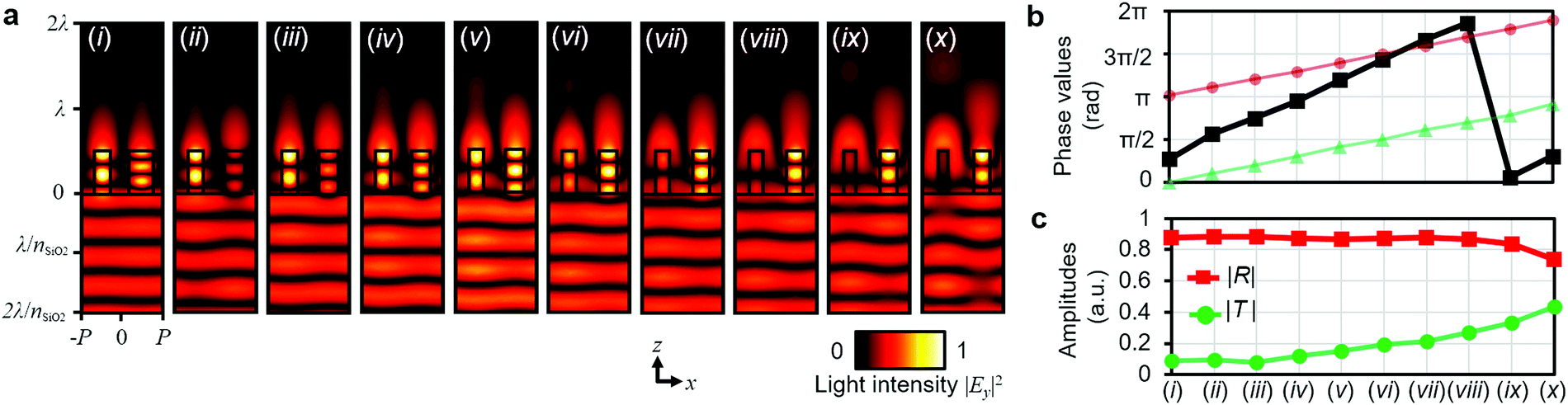
For a square pillar, which imparts the same phase shift values regardless of input polarization, the induced reflection is numerically demonstrated. The structural information was extracted from Fig. 1b, and their square widths were adopted to impart phase values showing out-of-phase conditions to each other. A total of ten structural parameter sets were adopted, and their phase values differed by π/10. The structural information (widths of the square nanopillars) is shown in Table S1 (ESI†). Because the phase values are doubled at the induced reflection, as shown in Fig. 2b, each nanopillar imparts the same phase shift to the reflection. As shown in Fig. 3a, most of the light intensity goes to the reflection spaces in all examples. The reflected phase shifts by two nanopillars are twice the gradient of the original phase shifts (Lφi when L = 2), as expected; this is shown in Fig. 3a and b. The light cannot proceed to the transmission space due to the abovementioned theory; therefore, the evanescent field can be observed, as shown in Fig. 3a. The corresponding reflection and transmission amplitudes are also calculated in Fig. 3c. The reason for the leakage to transmission is the mismatch of the transmission amplitudes of the original nanopillars and the relatively low light confinement in the nanopillars. The dispersive characteristics are also shown in Fig. S4 (ESI†) for five selected parameters. It is worth mentioning that in reflection, one may think that the wave can be coupled into diffraction orders of n = 1 and −1 in reflection space; however, this is possible if the light energy (i.e. induced current density, normalized magnetic energy), which dominates the scattering characteristics of each nanopillar, is not confined into the PGM but into the adjacent free space. This makes it difficult to generate the induced reflection, which contributes to the main reason for the mismatch between the analytical and numerical results. In our design, this means that if relatively low index materials (i.e. GaN, TiO2, GaP, etc.) are adopted, improved features can be realized.
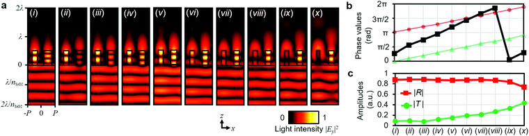 |
| | Fig. 3 Simulated results showing the induced reflection. (a) The light field intensity patterns from ten selected structural parameter sets. The electric field is incident from the bottom of the structure, directed in y. The interference pattern shows that the light is mostly reflected as expected. The square nanopillars in one set have phase values that are out-of-phase with each other, which means the phase gradient is identical. Their original phase values in transmission can be observed in (b), and the values increase while maintaining an identical phase gradient. The green triangles are phase values from the right nanopillar, and the red circles are phase values from the left nanopillar. The reflected phase values of (i − x) are also shown in black squares, which are two times the transmissive phase shift. (c) Transmission and reflection amplitudes from (i − x). The red squares are the reflection amplitudes and the green circles are the transmission amplitudes. | |
By using the design method discussed in the previous section and the induced reflection here, the metasurface was designed to operate like a polarizing beam splitter (PBS). Using the fact that one nanopillar can impart two independent phase values and a PGM can be used to induce reflection from the transmissive metasurface, two nanopillars were combined into one unit cell for realization of unprecedented operation in metasurfaces: firstly, this metasurface can split incident light into totally different spaces of transmission and reflection, distinguished by their polarization states. Previous studies succeeded in beam splitting by polarization; however, they hardly divided the beam trajectory into full space, especially in the optical frequency regime.14,15,25 Secondly, the phase shift value can be independently imparted to both spaces. This is possible through using linearly birefringent nanopillars, where the light reaction varies with the polarization state. As an example, assume that a designer wants to design a nanopillar that imparts the phase values of φ1 and φ2 into transmission and reflection, respectively, and at the same time, wants the light to be split on a linear polarization basis. Basically, for reflective operation, the unit structure should have two nanopillars. As discussed in this section, the two nanopillars are used for the generation of a phase gradient larger than the wavevector in free space. If x-polarization is chosen to occur at transmission, then the two nanopillars are designed to impart the identical phase of φ1 for x-polarized light. On the other hand, for y-polarized light, the two nanopillars need to operate in reflective mode. This is made possible by inducing the reflection of L = 2, which is realized by two nanopillars conveying the phases of φ2/2 and φ2/2 + π at y-polarization. Because these phase values give the same conditions discussed in this section, the induced reflection will have the phase value of φ2. In detail, simulation results with structural parameters are also provided in Fig. S5 (ESI†) in the case of the linear polarization basis. Because polarization-selective phase retardation is possible on an arbitrary polarization basis, as discussed the in previous section, polarization-selective full-space phase modulation is achievable. The dispersive characteristics of the proposed scheme calculated with selected parameters can be found in Fig. S6 (ESI†).
Experimental demonstration of the proposed scheme
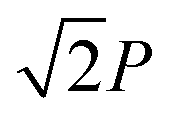
In this chapter, three types of metasurfaces were fabricated for experimental demonstration with discussion, distinguished by their operational polarization states. The three selected polarization pairs are expressed by the phase differences between the electric fields directed at the two principal axes, namely the x- and y-axes, and their values are 0, π/4 and π/2, respectively (see part 1 in the ESI†). The measurements were carried out with an optical setup, as shown in Fig. 4a. The polarizers at the output ends were sometimes selectively removed for the desired analysis. As mentioned in the above section, the unit cell consisted of two nanopillars, as shown in Fig. 4b and c. The unit cell structure was inclined at 45 degrees, as clearly shown in Fig. 4b, which was designed to shorten the period from 2P to  (see Fig. S7, ESI†). The samples were fabricated by standard electron beam lithography (for detailed information, refer to part 3 in the ESI†).
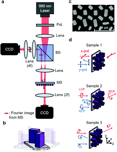 |
| | Fig. 4 (a) Schematic of the optical setup for capturing Fourier images of the fabricated samples with a diode laser of 980 nm wavelength. The input polarizers are subject to change according to their purposes. The two lenses before the metasurface are used for collimating the light, and the lenses after the metasurfaces are for the 2-f system for obtaining the Fourier image of the metasurface. MS: metasurface, CCD: charge-coupled device, BS: beam splitter, Pol.: polarizer. (b) Schematic of the unit cell composed of two rectangular nanopillars. (c) SEM image captured from the sample operating in the linear polarization pair. Scale bar: 1 μm. (d) Schematics of the three fabricated samples distinguished by the polarization pair in operation. For the beam steering and hologram generation samples, this notation is preserved. | |
We introduced two operational types for experimental verification of the proposed metasurface device: (1) one is a beam steering sample, which transmits light into transmission and reflection spaces by the input polarization states, and the steering angles at each space are also freely designed. (2) The other is a hologram generation sample, and the same basic design method was employed as with the above examples. However, we believe that this sample shows the elemental level of potential of this design scheme because the capacity for holographic generation indicates the possibility of other operations, such as orbital angular momentum and lensing. The method by which the trajectories of the three polarization types were determined is depicted in Fig. 4d: the sample operating in linear polarized light splits the x-polarized light into transmission space and the y-polarized light into reflection space. For the sample operating in circular polarization, the incident left-handed circularly polarized (LCP) light transmits to transmission space and the polarization is reversed, while the right-handed circularly polarized (RCP) light is reflected and reversed in polarization. In the case of the elliptical polarized light sample, the polarization direction is depicted as an in-plane arrow in Fig. 4d.
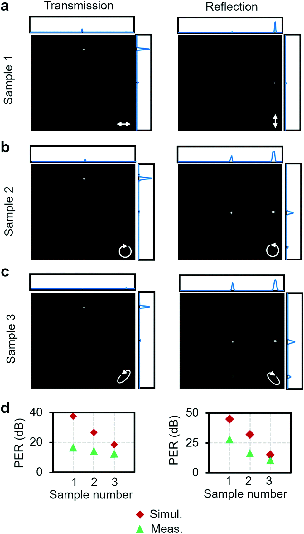
As the first example, we demonstrate the beam-steering capability of the proposed scheme. Each sample was fabricated with identical operation with phase gradient values of which in transmission space, the value is  in the +y direction, and in reflection space, it is
  in the +x direction. Consequently, one periodic structure is composed of a total of 10 × 8 × 2 meta-atoms. The structural information of the three samples can be found in Tables S2–S4 (ESI†). The samples were fabricated with a target size of 200 × 200 μm2, with about 700 meta-atoms in one line. Their operation was firstly verified by numerical simulation, conducted with a commercial finite domain time difference (FDTD) tool (Lumerical FDTD solutions). In the measurement step, the Fourier images were captured by a charge coupled device (CCD) camera to obtain the relative diffraction efficiency at each space. In both the simulations and experiments, the polarizers at input were altered, while the output polarizer was excluded to verify the beam splitting ability of the proposed scheme. As shown in Fig. 5a–c, the experimental result shows a desired operation with the preconditioned polarization state of incident light. The total efficiency of the reflection and transmission varies with different samples and polarizations, as can be found in Table 1, obtained by the FDTD results. The results show the possibility of use as novel PBS, considering the beams are divided into both spaces by the input polarization states. For analysis as a polarizing beam splitter, the polarization extinction ratio, defined as PER = Ppol.1/Ppol.2 (dB), was also calculated at the desired diffraction order (Fig. 5d). In our design, a PER can be obtained at both spaces, resulting in two PERs from one sample. At each space, Ppol.1 and Ppol.2 were measured at the same position to which the beam diffracted by the ideal sample propagates. That is, in transmission, the measured position is in the +y direction with a momentum of 0.444P. The subscript pol.1 indicates the wanted polarization state and pol.2 is the unwanted state, which is orthogonal to pol.1. For example, in transmission (reflection) mode, when the x(y)-polarized light impinges to sample 1, the efficiency of light which is diffracted in the +y(x) direction with a momentum of 0.444P (0.555P) is measured, and this is called Ppol1. Next, the input polarization is tuned to y(x)-polarized light; then, Ppol.2 is measured at the same position as before. We achieved PERs with maximum values of up to 16.7 dB at transmission and 27.8 dB at reflection in sample 1. The difference between the simulations and experiments is due to the imperfection of the optical elements used in the optical setup and fabrication error of the samples. Further results, including the intensity profiles and results with the output polarizer, can be found in Fig. S8–S10 (ESI†). This is notable in that the transmissive metasurface is utilized to send light into reflection spaces by a local phase gradient. A comparison between the efficiencies of the simulations and experiments is shown in Fig. S11 (ESI†), and they show great agreement with each other. The difference is mainly due to the inevitable reflection from the substrate, which is shown well in the reflection cases at the zeroth order. The dispersive characteristics of the PER were also calculated, as shown in Fig. S12 (ESI†).
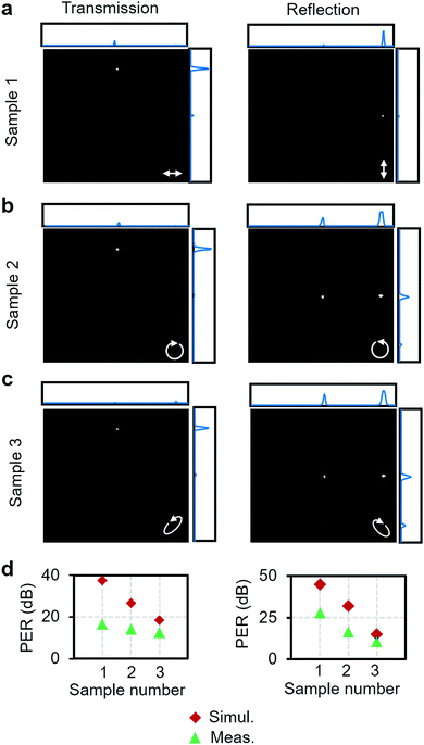 |
| | Fig. 5 Beam steering results from experiments: (a–c) CCD-captured images and the line graph extracted near the zeroth order diffraction, showing the experimental results of the diffraction order efficiency. (a) is from sample 1, operating in the linear polarization pair, (b) is from sample 2, operating in the circular polarization pair, and (c) is from sample 3, operating in the elliptical polarization pair. White arrows indicate the polarization states of the input light. (d) Polarization extinction ratios obtained from three fabricated samples. Simul.: simulation result, Meas.: measured result. | |
Table 1 Total diffraction efficiency obtained with FDTD results
| Sample number |
1 |
2 |
3 |
| Input polarization |
x-Pol |
y-Pol |
LCP |
RCP |
El1a |
El2 |
|
El1 (El2) is the elliptical polarization state determined to operate in transmission (reflection) mode.
The term in brackets is the efficiency at the target diffraction order.
|
| Total efficiency (%) |
Transmission |
79.34 (76.62)b |
21.44 |
80.46 (77.54) |
15.40 |
77.59 (73.93) |
21.41 |
| Reflection |
8.444 |
57.67 (38.56) |
9.376 |
65.37 (31.04) |
11.02 |
56.95 (14.67) |
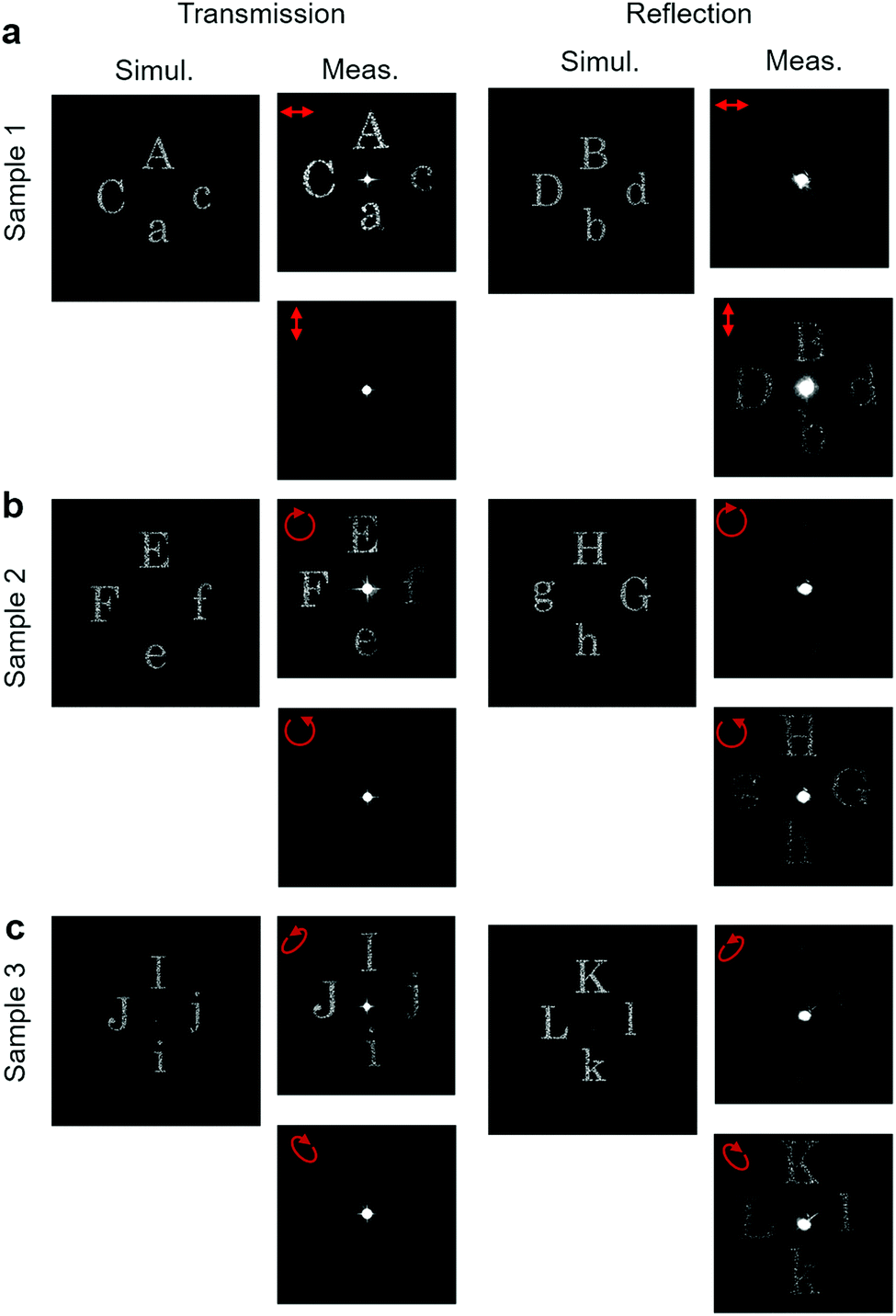
As the second example for experimental verification, asymmetric holographic image generation was demonstrated. That is, the holographic image itself as well as the space where it was generated were altered according to the polarization state. Three different samples were fabricated, which were distinguished by the operational polarization pair and generated holographic images as well. The fabricated sample is composed of 300 × 300 pixels, having 300 × 300 × 2 meta-atoms in total. Two target holographic images were encoded by the Gerchberg-Saxton algorithm to be regenerated at the Fourier plane; therefore, as shown in Fig. 4a, a lens is placed between the sample and CCD camera. At the encoding step, the image is designed to occupy the area which is determined considering the numerical aperture of the Fourier lens used in the measurement step in Fig. 4a, which is 0.5 (see Fig. S13, ESI†). The phase profiles and structural parameters of the three fabricated samples can be found in Fig. S14–S16 (ESI†). In the measurement step, the images are captured by the CCD camera by changing the polarization state of incident light. The captured images are shown in Fig. 6a–c on the right, described with the input polarization states, and the simulation results are shown on the left. The holograms generated in the transmission spaces have polarization states orthogonal to those of the holographic images in the reflection spaces. As shown in the measured results, when the opposite basis of polarized light is incident onto each sample, the holographic images can barely be discerned. In terms of the optical power, which is the integrated value except for the power at the middle of the resultant image, the ratio was calculated for each sample and space. This was determined by input polarization (Ppol.1/Ppol.2), like the PER above, but not in dB scale (Fig. S17, ESI†). The ER here shows a similar trend to the beam steering case. The maximum ratios were achieved for sample 1, namely 8.75 at transmission and 3.902 at reflection. In terms of image generation, the experimental results show good agreement with the simulation results. The hologram conversion efficiency is calculated numerically, assuming the incident light is plane wave and the near-field effect is neglected (Table 2). Considering the zeroth order term that is not found in the numerical result, the efficiency of the experimental results could be lower than that of the simulated results. The main reason for the difference is fabrication error, as the operation of the designed metasurface is dependent on the dimensions of the nanopillars. Also, the total beam profile occupies more area than the fabricated sample sizes, and this contributes to the increase of the zeroth order diffraction.
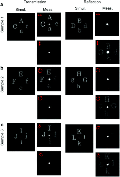 |
| | Fig. 6 Hologram generation results from simulations and measurements. From top to bottom, the holograms are operating in (a) linear (sample 1), (b) circular (sample 2), and (c) elliptical (sample 3) polarization states. The arrows indicate how the polarizer is directed at the input end. | |
Table 2 Numerically retrieved hologram conversion efficiencies
| Conversion efficiency [%] |
Sample 1 |
Sample 2 |
Sample 3 |
| Transmission |
80.01 |
79.87 |
66.42 |
| Reflection |
78.18 |
79.57 |
65.79 |
Conclusion
In conclusion, we designed and experimentally demonstrated metasurfaces which are capable of controlling the full space of incident light. Unlike previous studies, the controlled space is flipped by the polarization states of incident light, which is possible due to the linearly birefringent rectangular nanopillars and the integer parity design to realize induced reflection. Transmissive and linearly birefringent nanopillars were employed for distinct phase shifts to any pair of orthogonal polarization states, involving reversed handedness. Two nanopillars were multiplexed into a unit cell, and using GSL, the critical angle condition with normal incident light was used to mediate the reflective operation from transmissive PGM. Next, beam deflection and hologram generation samples were fabricated for experimental verification of the proposed scheme. For each operation, three samples operating in linear, circular and elliptical polarization pairs were fabricated. The results were in good agreement with the simulation results, demonstrating the potential of the metasurfaces to be utilized in various optical applications as novel PBS. In addition to PBS applications, the ability to design different beam trajectories according to polarization may be comparable with a polarization volume grating composed of liquid crystal. Their diffraction efficiency and polarization contrast can be larger than the metasurface; however, our scheme has merits of ultrathin thickness (∼λ) and subwavelength pixel pitch. The additional advantage of the proposed scheme with respect to currently employed spatial light modulators is that the proposed scheme is characterized by extremely compact features and capability of full-space modulation. Furthermore, in terms of vectorial holograms, i.e. multichannel holograms generated with various polarization states, this scheme could be used for demonstration of vectorial holographic images appearing in both spaces, which can be called 360° vectorial holograms.16,29 Adding the encryption method of ref. 16 to this scheme would allow the vectorial holographic images to be further encrypted in the generated space. Finally, in terms of applicability, we expect that this scheme can be more useful in designing novel optical setups and can be compatible in various conventional setups, which would lighten the weight of optical devices.41–44
Conflicts of interest
There are no conflicts of interest to declare.
Acknowledgements
This work was supported by the National Research Foundation of Korea (NRF) grant funded by the Korean Government (MSIT) (No. 2020R1A2B5B02002730).
References
- N. Yu and F. Capasso, Nat. Mater., 2014, 13, 139–150 Search PubMed.
- H.-T. Chen, A. J. Taylor and N. Yu, Rep. Prog. Phys., 2016, 79, 076401 Search PubMed.
- F. Ding, A. Pors and S. I. Bozhevolnyi, Rep. Prog. Phys., 2017, 81, 026401 Search PubMed.
- G.-Y. Lee, G. Yoon, S.-Y. Lee, H. Yun, J. Cho, K. Lee, H. Kim, J. Rho and B. Lee, Nanoscale, 2018, 10, 4237–4245 Search PubMed.
- S. M. Kamali, E. Arbabi, A. Arbabi and A. Faraon, J. Nanophotonics, 2018, 7, 1041–1068 Search PubMed.
- G.-Y. Lee, J. Sung and B. Lee, ETRI J., 2019, 41, 10–22 Search PubMed.
- J. Sung, G.-Y. Lee and B. Lee, J. Nanophotonics, 2019, 8, 1701–1718 Search PubMed.
- C. Choi, S. Lee, S. Mun, G.-Y. Lee, J. Sung, H. Yun, J. Yang, H. Kim, C. Hwang and B. Lee, Adv. Opt. Mater., 2019, 7, 1900171 Search PubMed.
- G.-Y. Lee, J. Sung and B. Lee, MRS Bull., 2020, 45, 202–209 Search PubMed.
- Q. Wei, L. Huang, T. Zentgraf and Y. Wang, J. Nanophotonics, 2020, 9, 987–1002 Search PubMed.
- W. T. Chen, A. Y. Zhu, J. Sisler, Y.-W. Huang, K. M. A. Yousef, E. Lee, C.-W. Qiu and F. Capasso, Nano Lett., 2018, 18, 7801–7808 Search PubMed.
- P. Genevet, F. Capasso, F. Aieta, M. Khorasaninejad and R. Devlin, Optica, 2017, 4, 139 Search PubMed.
- M. Khorasaninejad and F. Capasso, Science, 2017, 358, eaam8100 Search PubMed.
- A. Arbabi, Y. Horie, M. Bagheri and A. Faraon, Nat. Nanotechnol., 2015, 10, 937–943 Search PubMed.
- J. P. Balthasar Mueller, N. A. Rubin, R. C. Devlin, B. Groever and F. Capasso, Phys. Rev. Lett., 2017, 118, 113901 Search PubMed.
- R. Zhao, B. Sain, Q. Wei, C. Tang, X. Li, T. Weiss, L. Huang, Y. Wang and T. Zentgraf, Light: Sci. Appl., 2018, 7, 95 Search PubMed.
- M. Miscuglio, N. J. Borys, D. Spirito, B. Martín-García, R. P. Zaccaria, A. Weber-Bargioni, P. J. Schuck and R. Krahne, ACS Nano, 2019, 13, 5646–5654 Search PubMed.
- D. Wen, F. Yue, G. Li, G. Zheng, K. Chan, S. Chen, M. Chen, K. F. Li, P. W. H. Wong, K. W. Cheah, E. Yue Bun Pun, S. Zhang and X. Chen, Nat. Commun., 2015, 6, 8241 Search PubMed.
- B. Wang, F. Dong, Q.-T. Li, D. Yang, C. Sun, J. Chen, Z. Song, L. Xu, W. Chu, Y.-F. Xiao, Q. Gong and Y. Li, Nano Lett., 2016, 16, 5235–5240 Search PubMed.
- E. Arbabi, A. Arbabi, S. M. Kamali, Y. Horie and A. Faraon, Opt. Express, 2016, 24, 18468–18477 Search PubMed.
- E. Arbabi, A. Arbabi, S. M. Kamali, Y. Horie and A. Faraon, Sci. Rep., 2016, 6, 32803 Search PubMed.
- B. H. Chen, P. C. Wu, V.-C. Su, Y.-C. Lai, C. H. Chu, I. C. Lee, J.-W. Chen, Y. H. Chen, Y.-C. Lan, C.-H. Kuan and D. P. Tsai, Nano Lett., 2017, 17, 6345–6352 Search PubMed.
- E. Maguid, I. Yulevich, M. Yannai, V. Kleiner, M. L. Brongersma and E. Hasman, Light: Sci. Appl., 2017, 6, e17027 Search PubMed.
- K. T. P. Lim, H. Liu, Y. Liu and J. K. W. Yang, Nat. Commun., 2019, 10, 25 Search PubMed.
- T. Cai, G. Wang, S. Tang, H. Xu, J. Duan, H. Guo, F. Guan, S. Sun, Q. He and L. Zhou, Phys. Rev. Appl., 2017, 8, 034033 Search PubMed.
- L. Zhang, R. Y. Wu, G. D. Bai, H. T. Wu, Q. Ma, X. Q. Chen and T. J. Cui, Adv. Funct. Mater., 2018, 28, 1802205 Search PubMed.
- R. Y. Wu, L. Zhang, L. Bao, L. W. Wu, Q. Ma, G. D. Bai, H. T. Wu and T. J. Cui, Adv. Opt. Mater., 2019, 7, 1801429 Search PubMed.
- J. Sung, G.-Y. Lee, C. Choi, J. Hong and B. Lee, Adv. Opt. Mater., 2019, 7, 1801748 Search PubMed.
- X. Zhang, M. Pu, Y. Guo, J. Jin, X. Li, X. Ma, J. Luo, C. Wang and X. Luo, Adv. Funct. Mater., 2019, 29, 1809145 Search PubMed.
- F. Zhang, M. Pu, X. Li, P. Gao, X. Ma, J. Luo, H. Yu and X. Luo, Adv. Funct. Mater., 2017, 27, 1704295 Search PubMed.
- D. Lin, P. Fan, E. Hasman and M. L. Brongersma, Science, 2014, 345, 298–302 Search PubMed.
- S. Sun, K.-Y. Yang, C.-M. Wang, T.-K. Juan, W. T. Chen, C. Y. Liao, Q. He, S. Xiao, W.-T. Kung, G.-Y. Guo, L. Zhou and D. P. Tsai, Nano Lett., 2012, 12, 6223–6229 Search PubMed.
- Z. Li, M.-H. Kim, C. Wang, Z. Han, S. Shrestha, A. C. Overvig, M. Lu, A. Stein, A. M. Agarwal, M. Lončar and N. Yu, Nat. Nanotechnol., 2017, 12, 675–683 Search PubMed.
- N. Yu, P. Genevet, M. A. Kats, F. Aieta, J.-P. Tetienne, F. Capasso and Z. Gaburro, Science, 2011, 334, 333–337 Search PubMed.
- Y. Fu, C. Shen, Y. Cao, L. Gao, H. Chen, C. T. Chan, S. A. Cummer and Y. Xu, Nat. Commun., 2019, 10, 2326 Search PubMed.
- Y. Xu, Y. Fu and H. Chen, Sci. Rep., 2015, 5, 12219 Search PubMed.
- C. Shen and S. A. Cummer, Phys. Rev. Appl., 2018, 9, 054009 Search PubMed.
- Y. Cao, Y. Fu, Q. Zhou, X. Ou, L. Gao, H. Chen and Y. Xu, Phys. Rev. Appl., 2019, 12, 024006 Search PubMed.
- Y. Fu, J. Tao, A. Song, Y. Liu and Y. Xu, Front. Phys., 2020, 15, 52502 Search PubMed.
- S. Zhu, S. Zhu, Y. Cao, Y. Fu, Y. Fu, X. Li, L. Gao, L. Gao, H. Chen and Y. Xu, Opt. Lett., 2020, 45, 3989–3992 Search PubMed.
- G.-Y. Lee, J.-Y. Hong, S. Hwang, S. Moon, H. Kang, S. Jeon, H. Kim, J.-H. Jeong and B. Lee, Nat. Commun., 2018, 9, 4562 Search PubMed.
- C. Kim, S.-J. Kim and B. Lee, Opt. Express, 2020, 28, 18059–18076 Search PubMed.
- J. Sisler, W. T. Chen, A. Y. Zhu and F. Capasso, APL Photonics, 2020, 5, 056107 Search PubMed.
- H. Kwon, E. Arbabi, S. M. Kamali, M. Faraji-Dana and A. Faraon, Nat. Photonics, 2020, 14, 109–114 Search PubMed.
Footnote |
| † Electronic supplementary information (ESI) available. See DOI: 10.1039/d0nh00319k |
|
| This journal is © The Royal Society of Chemistry 2020 |
Click here to see how this site uses Cookies. View our privacy policy here. 
 Open Access Article
 This Open Access Article is licensed under a
  *
*
 (see Fig. S7, ESI†). The samples were fabricated by standard electron beam lithography (for detailed information, refer to part 3 in the ESI†).

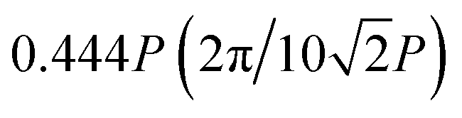 in the +y direction, and in reflection space, it is
 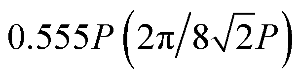 in the +x direction. Consequently, one periodic structure is composed of a total of 10 × 8 × 2 meta-atoms. The structural information of the three samples can be found in Tables S2–S4 (ESI†). The samples were fabricated with a target size of 200 × 200 μm2, with about 700 meta-atoms in one line. Their operation was firstly verified by numerical simulation, conducted with a commercial finite domain time difference (FDTD) tool (Lumerical FDTD solutions). In the measurement step, the Fourier images were captured by a charge coupled device (CCD) camera to obtain the relative diffraction efficiency at each space. In both the simulations and experiments, the polarizers at input were altered, while the output polarizer was excluded to verify the beam splitting ability of the proposed scheme. As shown in Fig. 5a–c, the experimental result shows a desired operation with the preconditioned polarization state of incident light. The total efficiency of the reflection and transmission varies with different samples and polarizations, as can be found in Table 1, obtained by the FDTD results. The results show the possibility of use as novel PBS, considering the beams are divided into both spaces by the input polarization states. For analysis as a polarizing beam splitter, the polarization extinction ratio, defined as PER = Ppol.1/Ppol.2 (dB), was also calculated at the desired diffraction order (Fig. 5d). In our design, a PER can be obtained at both spaces, resulting in two PERs from one sample. At each space, Ppol.1 and Ppol.2 were measured at the same position to which the beam diffracted by the ideal sample propagates. That is, in transmission, the measured position is in the +y direction with a momentum of 0.444P. The subscript pol.1 indicates the wanted polarization state and pol.2 is the unwanted state, which is orthogonal to pol.1. For example, in transmission (reflection) mode, when the x(y)-polarized light impinges to sample 1, the efficiency of light which is diffracted in the +y(x) direction with a momentum of 0.444P (0.555P) is measured, and this is called Ppol1. Next, the input polarization is tuned to y(x)-polarized light; then, Ppol.2 is measured at the same position as before. We achieved PERs with maximum values of up to 16.7 dB at transmission and 27.8 dB at reflection in sample 1. The difference between the simulations and experiments is due to the imperfection of the optical elements used in the optical setup and fabrication error of the samples. Further results, including the intensity profiles and results with the output polarizer, can be found in Fig. S8–S10 (ESI†). This is notable in that the transmissive metasurface is utilized to send light into reflection spaces by a local phase gradient. A comparison between the efficiencies of the simulations and experiments is shown in Fig. S11 (ESI†), and they show great agreement with each other. The difference is mainly due to the inevitable reflection from the substrate, which is shown well in the reflection cases at the zeroth order. The dispersive characteristics of the PER were also calculated, as shown in Fig. S12 (ESI†).