
Enhancement of exciton emission in WS2 based on the Kerker effect from the mode engineering of individual Si nanostripes†
Jiahao
Yan
 a,
Zhaoqiang
Zheng
b,
Zaizhu
Lou
a,
Juan
Li
a,
Bijun
Mao
a and
Baojun
Li
*a
a,
Zhaoqiang
Zheng
b,
Zaizhu
Lou
a,
Juan
Li
a,
Bijun
Mao
a and
Baojun
Li
*a
aInstitute of Nanophotonics, Jinan University, Guangzhou 511443, China. E-mail: baojunli@jnu.edu.cn
bSchool of Materials and Energy, Guangdong University of Technology, Guangzhou 510006, China
First published on 22nd June 2020
Abstract
Coupling between nanostructures and excitons has attracted great attention for potential applications in quantum information technology. Compared with plasmonic platforms, all-dielectric nanostructures with Mie resonances are more practical because of low-loss, low-cost and CMOS compatibility. However, weak field enhancements in single element dielectric nanostructures hinder their applications in both strong and weak coupling regimes. The Kerker effect arising from the far-field electro-magnetic interactions in dielectric nanostructures brings a new mechanism to realize effective coupling with excitons. Until now, it still remains unsolved whether effective Mie-exciton coupling can be realized based on pure far-field Kerker effect. Therefore, we proposed a silicon-on-insulator (SOI) integrated Mie resonator with a 135 nm top oxide layer to exclude the near-field coupling between excitons and silicon (Si) nanostripes. Through tuning the widths of Si nanostripes to obtain highly directional photoluminescence (PL) emission under Kerker conditions, strong PL enhancements can be observed, whose enhancement factors are comparable to the reported best performances of single all-dielectric or even plasmonic nanostructures coupling with 2D excitons. Our findings bring new strategies for strong light–matter interactions with near-zero heating loss and make it possible to construct 2D materials–silicon hybrid integration for future nanophotonic and optoelectronic devices.
New conceptsAll-dielectric nanostructures with Mie-type magnetic and electric resonant modes have attracted intense research interest. Compared with plasmonic platforms, all-dielectric Mie resonators are more practical for realizing effective coupling with excitons because of low-loss, low-cost and CMOS compatibility. The Kerker effect arising from the far-field electro-magnetic interactions in dielectric nanostructures brings a new mechanism to realize effective coupling with excitons. Until now, it still remains unsolved if strong PL enhancement can be realized based on pure far-field Kerker effect. In this work, we proposed a brand new SOI based Mie resonator: a Si nanostripe with a 135 nm thick top oxide layer. The presence of an oxide spacer totally blocks the near-field enhancements of Si nanostripes and helps obtain the pure Kerker effect PL enhancements. The maximum PL enhancement factor of monolayer WS2 on the Si nanostripes is about 3.2 and that of bilayer WS2 is about 4. To our knowledge, it is comparable to the best enhancement performance of single dielectric nanostructures. Our findings bring new strategies for strong light–matter interactions with near-zero heating loss and make it possible to construct 2D materials–silicon hybrid integration for future nanophotonics and optoelectronic devices. |
The manipulation of the phase, amplitude and wavelength of the light field is the basis for light–matter interactions, and the development of new materials has promoted effective light–matter interactions. For example, the enhancement of nonlinear effects has been realized through photonic crystals1 and epsilon-near-zero materials.2 Plasmonic nanostructures with a strong near-field enhancement have made it possible to do optical near-field patterning.3 In contrast, all-dielectric nanostructures with fascinating far-field properties and low-cost and low-loss features have attracted intense research interest recently.4,5 All-dielectric nanoantennas made from high-refractive index materials with Mie-type magnetic and electric resonant modes can modulate the light radiation directionally.6 Moreover, metasurfaces formed by dielectric nano-resonators show great applications in nonlinear optics,7 biomedical,8 imaging9 and electro-optic modulation.10,11 All-dielectric metasurfaces also exhibit effective wavefront control to generate or process orbital angular momentum beams.12,13 Very recently, the coupling between excitons (especially 2D excitons) and dielectric Mie resonators has drawn researchers’ attention due to the different resonant modes14 compared with plasmonic nanostructures.15–17 Although high Q modes can be realized in the well-designed dielectric arrays,18–21 for single dielectric structures, high Q, small mode volumes or strong coupling strength (g) cannot be easily obtained22,23 to realize obvious Purcell effects or Rabi splitting because of the much weaker and internally-distributed resonant modes24 compared with plasmonic resonances. For a weak coupling regime, PL enhancement with no more than twice or even PL quenching was observed in single Si nanostructures.25,26 Even for gratings, the enhancement factors were less than 10.27–29 For a strong coupling regime, only unobvious Rabi splitting was demonstrated via the coupling of Si nanoparticles24,30,31 with 2D-excitons. Therefore, a new mechanism is urgently needed for effective light–matter interactions based on dielectric nanostructures.
The Kerker condition was first proposed by M. Kerker et al.32 to study the zero backward or forward scattering arising from the interference between electric and magnetic dipole modes based on the Mie coefficients. This theory can be expanded to study the directional scattering from dielectric nanostructures with arbitrary shapes containing multipole electric and magnetic resonant modes.33,34 Using the Kerker condition to build Huygens’ metasurfaces gives more complex functionalities to light.10 Therefore, The Kerker condition brings a new mechanism for the coupling between 2D excitons and dielectric nanostructures. However, it still remains unclear if we can realize significant PL enhancements based on pure far-field Kerker effects. Monolayer 2D materials in all previous studies were contacted with dielectric nanostructures directly, which cannot clarify whether the conventional near-field effect or Kerker effect contributes to the PL manipulation. Therefore, it is very important to study the Mie-exciton coupling and obtain strong PL enhancements based on pure Kerker effects.
Here, we proposed an SOI based Mie resonator: a Si nanostripe with a bottom oxide layer and a 135 nm top oxide layer. Hybrid structures were fabricated through placing monolayer and bilayer tungsten disulfide (WS2) on Si nanostripes with different widths, and the existence of an oxide spacer for applying gate voltages would be crucial for building WS2-based field-effect transistors.35 More importantly, the presence of an oxide spacer blocks the near-field enhancements and heating effects of Si nanostripes and helps obtain the pure Kerker effect PL enhancements. In experiments, the maximum PL enhancement factor of monolayer WS2 on the Si nanostripes is about 3.2 and that of bilayer WS2 is about 4. To our knowledge, it is the best enhancement performance of single dielectric nanostructures,25,26 and it is even better than many single plasmonic nanostructures.36–39 Moreover, the pure far-field effect greatly inhibited the Joule heating which is inevitable for plasmonic platforms. In theory, dipole sources were used to simulate the excitonic emission from WS2 layers, and we found that the Kerker conditions and top/bottom (T/B) radiation ratios change a lot with the widths of the Si nanostripes and the thickness of the oxide spacer. Through optimizing the Kerker condition and obtaining the largest T/B ratio, we observed strong PL enhancements without near-field enhancements and large Q. The proposed new mechanism of the effective coupling between 2D excitons and Mie resonators will greatly inspire the design of SOI-integrated TMDC-based photonic and optoelectronic circuits in the future.
Results and discussion
A schematic of a SOI-based Mie resonator is shown in Fig. 1a. The purchased SOI wafer has an oxide layer with a thickness of 375 nm and a top Si layer with a thickness of 200 nm. Electron beam lithography (EBL) was used to fabricate Si nanostripes with different widths. Because hydrogen silsesquioxane (HSQ) was used as the resist during the EBL process, a top oxide layer was formed on Si nanostripes after the exposure and etching processes. Fig. 1b shows the strategy of studying the coupling between Si nanostripes and 2D excitons in WS2. Two types of incidence were used in optical measurements: white light and a 514 nm laser. Under excitation, optical signals decay backward or forward, and the backward dark-field scattering and backward PL signals are collected. To determine the thickness of the top oxide layer formed from HSQ resists, atomic force microscope (AFM) images and height profiles are presented in Fig. 1c and d and Fig. S1 (ESI†). The height of the SiO2/Si nanostripes is around 335 nm. Since the redundant silicon was fully etched as shown in the optical image (Fig. S2, ESI†), the thickness of the top oxide layer is determined as 135 nm. As we know, Mie-type resonances of all-dielectric nanostructures were usually studied in free space or on pure oxide substrates, and the oxide layer with finite thickness may generate Fabry–Perot (F–P) modes and influence the scattering spectra.24,40 To clarify this, oxide thickness-dependent scattering spectra under two polarization directions were simulated as shown in Fig. S3 (ESI†) and Fig. 1e and f. From Fig. S3 (ESI†), we can conclude that the thickness of the bottom oxide layer does affect the scattering intensity but has little influence on the locations of resonant peaks. In our case, the F–P mode from SOI substrates with a 375 nm bottom oxide layer has constructive interference with the Mie resonances and thus enhances the optical responses. More simulations with thicker bottom oxide layers were conducted, which show more obvious F–P interferences (Fig. S4, ESI†). Although the single crystal Si film on the silica substrate is better to obtain pure Mie resonant modes, the study on SOI substrates is meaningful and necessary for the future optoelectronic integration.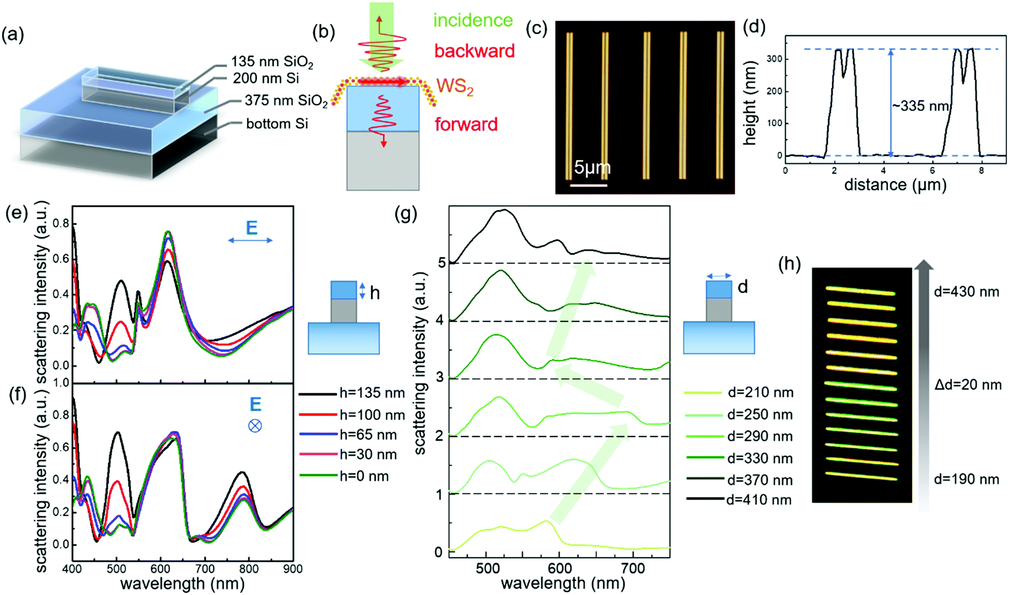 | ||
| Fig. 1 Optical resonant modes in SOI-integrated Si nanostripes. (a) Schematic showing the cross section of a Si nanostripe with a top oxide layer. (b) Schematic showing the coupling between WS2 layers and Si nanostripes, and the forward and backward radiation under incidence. (c and d) The AFM image and the corresponding height profile of Si nanostripes. (e and f) Simulated scattering spectra of Si nanostripes with the width of 210 nm and varied thicknesses of the top oxide layer under perpendicular (e) and parallel (f) polarized incident light. (g) Simulated width-dependent scattering spectra of nanostripes. (h) The dark-field optical image of fabricated nanostripes with varied widths. | ||
After adding the top oxide layer with various thicknesses from 0 to 135 nm (Fig. 1e and f), the scattering spectra exhibit slight changes except for the peak around λ = 500 nm. Fig. 1g plots the width-dependent scattering spectra of the fabricated Si nanostripes with a 135 nm top oxide layer, and the arrows show the change of the dominant mode at 550 nm < λ < 750 nm. The resonant modes in nanostripes are more complicated than spherical Mie resonators, because the spectral evolution with increasing widths is described by a series of multipole resonant modes. The red-shift of quadrupole resonant modes out of the visible range and the red-shift of the higher order modes in the visible range bring a red-blue-red shift behavior of the dominant scattering peak as illustrated by the arrows in Fig. 1g. This phenomenon was also observed for bare Si nanostripes with the same widths on pure silica as shown in Fig. S5 (ESI†). The collected dark-field images shown in Fig. 1h confirm this variation trend. From d = 190 to 430 nm with a 20 nm step size, the scattered color of the nanostripe changes from yellow to green and switches back to yellow again. It should be noticed that the variation trend of scattering peaks (Fig. 1g) cannot strictly simulate the scattered color because of different incident angles between experiments and simulations (see Methods).
To study the resonant modes of SOI-integrated Si nanostripes and the mode couplings, the simulated backward and forward scattering spectra of the fabricated Si nanostripes with the width of 250 nm are presented in Fig. 2a with a larger wavelength range (300 nm to 1300 nm). Based on the near-field profiles (Fig. 2d and e) at multiple resonant peaks, the magnetic dipole (MD) and electric dipole (ED) modes are located at the near infrared for both polarization directions as marked in Fig. 2a. From 900 nm to 450 nm, the resonant peaks are contributed by magnetic quadrupole (MQ), electric quadrupole (EQ), MD and EQ modes in turn.41 From the field distributions (Fig. 2d and e), the multipole features of these resonant peaks can be clearly seen. The partially overlapped higher order modes produce the Kerker effects and the directional scattering. For the fabricated Si nanostripes, the directivity is quite similar to other simple Mie resonators such as Si nanospheres42 and nanowires.43 The resonant peaks in the backward and forward directions are staggered, and the backward and forward scattering is dominated at different wavelength ranges. Similar directional scattering was also observed for the SiO2/Si nanostripe with a 210 nm width (Fig. 2b), and all resonant modes blue-shifted. The overlap degree and the coupling situation of magnetic and electric modes can be further modified when two nanostripes are placed together as a dimer structure (Fig. 2c). For the dimer structure with an 80 nm gap, the directivities at EQ and MQ wavelengths enhance under vertical polarization, while the directivities at ED, MQ and MD wavelengths enhance under parallel polarization. The simulated backward and forward scattering spectra for the dimer structure with a 40 nm gap (Fig. S6, ESI†) give a more intuitive comparison of the mode changes. The correspondence between dips and peaks was observed, which arises from the broadening of electric modes.33
 | ||
| Fig. 2 Coupling of resonant modes in the Si nanostripes. (a and b) Simulated forward and backward scattering spectra of the fabricated Si nanostripes with a width of 250 nm (a) and 210 nm (b) under perpendicular or parallel polarized incident light. The locations of resonant modes are labelled and marked with vertical bars. (c) Simulated forward and backward scattering spectra of the fabricated Si nanostripe dimer with the width of 210 nm and the gap of 80 nm under two orthogonal polarizations. Blue arrows showing the enhancement of directivity. (d and e) Electric and magnetic field profiles under perpendicular (d) and parallel (e) polarized incident light showing the multipole electric and magnetic resonant modes. The colors of background boxes correspond to the colors of vertical bars in (a). | ||
Monolayer WS2 was obtained through mechanical exfoliation and transferred onto Si nanostripes with different widths. Bright field optical images and scanning electron microscope (SEM) images (Fig. 3a–d) present the typical WS2 monolayers on Si nanostripes with widths of 210, 250, 350 and 390 nm. Dashed rectangular boxes indicate the regions where we have conducted multiple measurements. The dark-field scattering spectra of WS2–Si hybrid nanostructures were measured (Fig. 3e). Unexpectedly, the scattering from Si nanostripes with WS2 is stronger than that without WS2. As we know, the absorption of monolayer WS2 should have weakened the total scattering. The increase of scattering intensity here is ascribed to the existence of a top oxide layer, which weakens the near-field absorption. In addition, monolayer WS2 can act as a 2D dipole resonator which generates Kerker-type interferences with the multipole resonant modes in the Si nanostripe and enhances the backward scattering. This phenomenon was confirmed through simulations (Fig. S7, ESI†) where WS2 monolayers were modeled as a trapezoid shape covering over the nanostripes. The enhanced scattering in simulated spectra was observed in some wavelength ranges, which is partially in accordance with the measured scattering spectra. The oblique incidence in experiments and the normal incidence with the total-field scattered-field (TFSF) source in simulations (see Methods) lead to the lineshape mismatch inevitably. To examine the influence of incident angles, the simulations based on oblique incidence (53°) were also conducted using wavelength scanning with a step size of 20 nm (Fig. S8, ESI†). Although the incident angle influences the intensities of resonant modes, the locations of resonant modes have no significant change.
 | ||
| Fig. 3 PL enhancements of monolayer WS2 coupling with Si nanostripes. (a–d) Optical and SEM images showing the monolayer WS2 on Si nanostripes with different widths. Dashed boxes mark the ranges of PL measurement. (e) Measured dark-field scattering spectra of Si nanostripes with and without monolayer WS2. (f) PL spectra of monolayer WS2 on nanostripes with different widths and on the regions without nanostripes. (g) Width-dependent PL enhancement performances and error bars showing the standard deviations. (h) PL enhancements of monolayer WS2 on the nanostripe dimer with a 210 nm width and an 80 nm gap. (i) The optical and SEM images of typical monolayer WS2 on the nanostripe dimer. The dashed box shows the PL mapping region. (j) PL mapping images of monolayer WS2 on a single Si nanostripe with the width of 210 nm and the nanostripe dimer with the width of 210 nm. | ||
PL intensities of WS2 monolayers on different Si nanostripes were measured (Fig. 3f). All kinds of Si nanostripes can enhance the PL intensity. Particularly for the Si nanostripe with a 250 nm width, the PL intensity is doubled. Although the measured PL enhancement factor cannot be comparable with some well-designed metasurfaces or photonic crystals, it is large enough for single dielectric nanostructures. The width-dependent PL intensities and standard deviations were plotted in Fig. 3g. For every region, we scanned the laser spot on the Si nanostripes and measured the PL spectra more than 10 times (specific numbers depend on the lengths of WS2 layers on nanostripes). The standard deviation was caused by the following factors inevitably: the deviation of the laser beam from the center of the nanostripe, which leads to different coverage areas and overall PL enhancements, varied tensile strains at different locations and different quantum yields on the edges or at the center of the WS2 layers. In Fig. S9 (ESI†), the PL spectra of monolayer WS2 with and without Si nanostripes were presented separately. Monolayer WS2 placed on two Si nanostripe dimers with the same width of 210 nm and an 80 nm gap distance was also investigated as shown in Fig. 3h. The nanostripe dimers exhibit enhanced PL intensity with the enhancement factors in the range from 2.5 to 3.2, larger than that of a single Si nanostripe with a 210 nm width. Optical and SEM images of the typical Si nanostripe dimer are shown in Fig. 3i. Besides, the 2D PL mapping images of the single Si nanostripe and the nanostripe dimer were also measured under the excitation wavelength of 532 nm (Fig. 3j) indicating that the dimer structure has a superior PL enhancement effect. To exclude the influences of defects and strains on the PL comparison, we measured the Raman spectra at exact locations where the PL were measured (Fig. S10, ESI†). There was no significant shift or splitting of the Raman peaks, which indicates that the transfer of WS2 layers onto Si nanostripes has little influence on the phonon energy and the lattice vibration.
The coupling between bilayer WS2 and Si nanostripes was also studied as shown in Fig. 4a and b. The dashed boxes in the optical images indicate the regions of SEM images, and the dashed boxes in the SEM images describe the PL measurement ranges. Besides single nanostripes and dimers, arrays containing ten Si nanostripes were also investigated as shown in Fig. 4c. From the PL intensities of bilayer WS2 on single nanostripes in Fig. 4d, the 210 nm width nanostripe can double the indirect excitonic emission, while no enhancement effect was observed at the direct excitonic wavelength. In contrast, Si nanostripes with the widths of 350 and 390 nm can double the direct band emission, while the enhancement factor of indirect band emission is smaller than that of the 210 nm nanostripe. For dimer structures as shown in Fig. 4e, the PL enhancements are stronger than single nanostripes especially at the direct excitonic peak. The indirect excitonic peaks doubled for both the 210 and 310 nm dimers, and the direct PL intensity of the 310 nm width dimer is almost four times larger than that without nanostripe dimer. PL enhancement performance can be further improved via combining more nanostripes as shown in Fig. 4f. The array with 210 nm width nanostripes and 80 nm gaps can double the direct PL intensity and enhance the indirect PL emission five times. Moreover, the array with 230 nm nanostripes can realize nearly tenfold direct band PL enhancement and sixfold indirect band PL enhancement. Although the sizes of the nanostripes in the arrays are close to each other, the enhancement factors and the spectral lineshapes are very different. For trilayer WS2 provided in Fig. S11 (ESI†), strong PL enhancement along with obvious spectral change was observed at both direct and indirect bands. To visualize the enhancement factors, Fig. 4g is presented to compare the PL enhancements of different structures.
 | ||
| Fig. 4 PL enhancements of bilayer WS2 coupling with Si nanostripes. (a–c) Optical and SEM images of bilayer WS2 on nanostripes with varied widths and numbers. (d) PL enhancements of bilayer WS2 on single Si nanostripes. (e) PL enhancements of bilayer WS2 on nanostripe dimers. (f) PL enhancements of bilayer WS2 on arrays containing 10 nanostripes. (g) The width-dependent PL enhancement factors and the standard deviations. | ||
As mentioned above, near-field enhancements from nanostripes with different widths have little influence on the coupling with WS2 layers because of the existence of a 135 nm top oxide layer. Therefore, there must be a new far-field mechanism that leads to different PL enhancement performances. Based on previous studies, scattering from arbitrary dielectric nanostructures can be decomposed by multipole electro-magnetic modes.44,45 For the multipole mode dominated scatterer, Kerker theory for electric and magnetic dipoles46 can be expanded to analyse the multipole interferences via the equation as follows:47
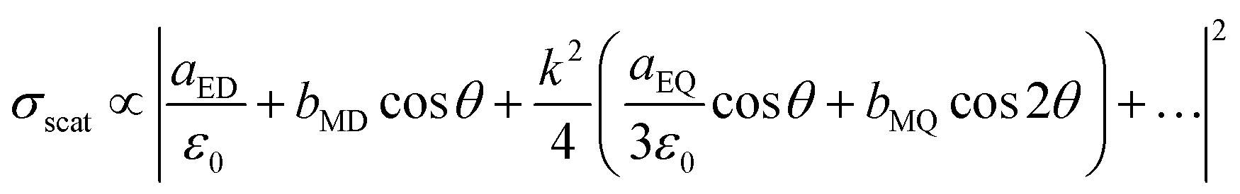 | (1) |
 | (2) |
The Purcell factor is defined as the ratio between the emission rate in a cavity (ΓC) and in free space (ΓO):23
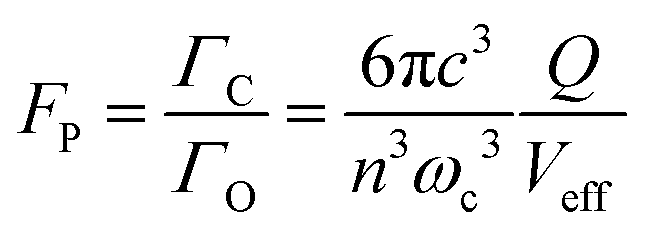 | (3) |
Simulated results in Fig. 5a illustrate the radiation directivity changing with the distance between the dipole source and the Si nanostripe. The bottom emission from a dipole source increases dramatically while the top emission decreases when changing the thickness of the top oxide layer from 135 nm to 0 nm. Since our detector was placed at the top, the 135 nm-oxide layer is beneficial for collecting more PL signals. In simulation, a single dipole emitter was put at the center of a nanostripe. Simulated spectra in Fig. S13 (ESI†) explain that the top emission does have some changes in intensity but has little change in lineshape when moving the single dipole emitter from the center to the edge. Therefore, in this part, a center dipole emitter was used to simplify the analysis. In Fig. 5b–e, a comparison between top and bottom emission under different polarization directions is presented. For the vertically polarized dipole emitter on the 210 nm Si nanostripe with an oxide layer, the top and bottom emission have similar intensity but exhibit the feature of Kerker scattering where the scattering peaks of the top detector correspond to the scattering dips of the bottom plane and vice versa. Similarly, for the parallelly polarized dipole emitter on the 210 nm Si nanostripe with an oxide layer, we also observed typical Kerker scattering and the dominant emission direction was changed with wavelength. However, for the dipole emitter on the 210 nm width Si nanostripe without a top oxide layer, the bottom emission is much stronger than the top emission under both linear polarization directions, which goes against the PL enhancement at the top plane. Moreover, the lineshapes of the top and bottom are very similar to each other which means no Kerker condition was observed. The near-field distributions of Si nanostripes with and without oxide layers under dipole source excitation (Fig. S14, ESI†) clearly indicate the different resonant modes. For the dipole–nanostripe structure with a 135 nm oxide layer, the electric and magnetic resonant modes are similar to the case of plane wave incidence. Therefore, Kerker conditions were observed. While for the direct combination between the dipole source and the nanostripe, the field intensities inside the nanostripes distribute unevenly, which damages the electric and magnetic multipole modes. To confirm the influence of oxide thickness, Si nanostripes without a top oxide layer and with a 30 nm thickness oxide layer were fabricated and measured as shown in Fig. S15 (ESI†). For monolayer WS2 on Si nanostripes with a 30 nm thickness oxide layer, there is no obvious change in PL intensity. While for WS2 on bare Si nanostripes, the PL emission even quenches.
 | ||
| Fig. 5 The generation of Kerker conditions based on the thickness of the top oxide layer. (a) A schematic showing the top and bottom detectors when using a dipole source, and the simulated top and bottom scattering efficiencies of nanostripes with different thicknesses of the top oxide layer. (b and c) Scattering efficiencies on the top and bottom planes from a single dipole source with vertical (b) and parallel (c) polarizations placed on the Si nanostripe with a 135 nm top oxide layer. Vertical bars and insets show the most obvious Kerker condition wavelengths. (d and e) Scattering efficiencies from a single dipole source with vertical (d) and parallel (e) polarizations placed on the bare Si nanostripe. | ||
To compare the Kerker effects of Si nanostripes with different widths more precisely, we used the array of dipole sources in simulation as shown in Fig. 6a. The simulated top and bottom emissions of excitons coupling with different Si nanostripes studied in Fig. 3 and 4 are presented in Fig. 6b–e with three lines to label the locations of direct exciton of the monolayer, direct exciton of the bilayer and indirect exciton of the bilayer, respectively. As mentioned above, the ratio between top emission and bottom emission (T/B) determines the PL enhancement factors; therefore, we need to examine the T/B ratio of different Si nanostripes. Horizontal bars in all figures mark the scattering efficiency at the top or bottom planes for comparison. For the direct excitonic emission of monolayer WS2, the T/B ratio under vertical (parallel) polarization for single Si nanostripes with widths of 210 nm, 250 nm, 350 nm and 390 nm is 1.4 (1.2), 2.4 (5.6), 2.3 (2.5) and 2.1 (2.1). The variation trends of T/B ratio agree with the performances of PL enhancement shown in Fig. 3g. For the monolayer WS2 on the 210 nm width nanostripe dimer, the T/B emission ratio is 3.6 for vertical polarization and 1.4 for parallel polarization, which is much larger than that of the single 210 nm width nanostripe. That is why the PL enhancement for the dimer structure is better than single nanostripes. From Fig. 6b and c, we can also conclude that the T/B ratio of direct excitonic emission in bilayer WS2 on Si nanostripes with 210 nm, 350 nm and 390 nm is 1.0, 2.3 and 2.1 under vertical polarization and 1.3, 2.5 and 2.6 under parallel polarization. While for the indirect excitonic emission of bilayer WS2 at λ = 710 nm, the T/B ratio for 210 nm, 350 nm and 390 nm nanostripes under vertical (parallel) polarization is 0.6 (0.8), 0.7 (0.4) and 0.7 (0.4), respectively. Therefore, Si nanostripes with the widths of 350 nm and 390 nm have better performance in direct band emission enhancement and worse performance in indirect band emission enhancement. Dimer and array structures further increase the T/B ratio as shown in Fig. 6d and e: the T/B ratio at direct band emission of the 210 nm dimer, 310 nm dimer, 210 nm array and 230 nm array under parallel (vertical) polarization is 1.9 (1.2), 3.6 (3.8), 1.8 (2.1) and 3.2 (5.7). Similarly, the T/B ratio at indirect band under parallel (vertical) polarization is 1.4 (0.8), 0.6 (0.8), 0.7 (1.0) and 2.3 (0.8) respectively. The improvement of directivity using arrays arises from the coupling between grating modes and the Mie resonant modes.49 Through the simulated reflections and transmissions of Si nanostripe arrays with different periodicities (Fig. S16, ESI†), the shift of electric and magnetic resonant modes can be clearly seen. Moreover, directivity can be enhanced in some wavelength ranges with “zero” transmission and “perfect” reflection. Radiation patterns of top and bottom emissions (Fig. S17 and S18, ESI†) indicate that a major portion of emission confines within 40°, which can be effectively collected by the objective with NA = 0.75.
 | ||
| Fig. 6 Kerker conditions based on the widths of Si nanostripes. (a) Schematic showing the simulation strategy and the wavelengths that we need to compare the T/B ratio. (b–e) Directional emission of dipole sources on top and bottom planes placed around Si nanostripes with different widths and numbers. Vertical and horizontal bars indicate the locations of excitonic emission and the T/B ratios. (f) Measured PL enhancement factors, calculated overall enhancement factors and directional enhancement factors of all samples. | ||
In order to compare the directional emission under Kerker effects and the performances of PL enhancements quantitatively, all factors including directivity, Purcell factors, laser spot size and absorption at the excitation wavelength (514 nm) were considered and calculated (Table S1, ESI†). The emission directivities were obtained from the simulated T/B ratios in Fig. 6b–e, the Purcell factors were obtained from the lifetime measurement in Fig. S12 (ESI†), and the absorption at 514 nm depended on the simulated field enhancements at the location of the WS2 layers. In general, the calculated enhancement factors show good agreement with the measured PL enhancement factors (Fig. 6f), and the emission directivity was confirmed as the dominant factor. The measured PL enhancement factors were also compared with other published studies based on plasmonic or dielectric nanostructures (Table S2, ESI†). For individual nanoantennas, the enhancement factors of the Si nanostripes from 1 to 4 are comparable to the best reported performance of single dielectric nanoantennas and are also high enough compared with some plasmonic nanoantennas. Moreover, the lowest non-radiative loss was obtained because of the far-field dominated mechanism. Compared with arrays and some well-designed nanoantennas with “hot-spots”, the enhancement factors of Si nanostripe arrays are moderate, which can be further increased via far-field and near-field engineering in the future.
Conclusions
In conclusion, we have demonstrated strong PL enhancements by pure far-field effects based on Kerker conditions. In experiments, we fabricated and studied the multipole electric and magnetic resonant modes in Si nanostripes, and the 135 nm top oxide layer was used to block near-field interactions between 2D excitons and Mie-type resonances. Through assembling monolayer and bilayer WS2 on Si nanostripes with different widths, we found that the widths and numbers of nanostripes strongly influence the intensities of both direct and indirect exciton emission. In theory, emission directivity from dipole sources was studied, and we have explained how different widths of nanostripes and thicknesses of oxide layers determine the T/B ratio. Our proposed mechanism on the coupling between Mie resonators and 2D excitons will benefit the effective light–matter interactions based on far-field effects and inspire the design of low-loss, low-cost and CMOS-compatible photonic devices. In the future, the performance of PL enhancement can be further improved through engineering both far-field directivity and near-field enhancement.Methods
Fabrication of Si nanostripes and transfer of WS2 flakes
First, the Si nanostripes with widths from 190 nm to 430 nm were fabricated on a purchased SOI wafer comprising a 200 nm thick silicon layer on a 375 nm thick oxide layer. Using EBL (Raith Vistec EBPG5000+ 100 kV), the pattern was defined in a HSQ electron beam resist which is spun on the top of the SOI wafer. After post baking and development, the inductively coupled plasma was used to fully etch the spare silicon, and residues of HSQ resist formed a 135 nm oxide layer on top of the Si nanostripes. Second, WS2 monolayers or bilayers obtained by mechanical exfoliation using Nitto blue tape were transferred to the viscoelastic PDMS substrate. Then, the transparent PDMS substrate was turned upside down and aligned on the Si nanostripes. Finally, the top PDMS was pressed to let it attach to the substrate and peeled off slowly.Dark-field scattering and PL measurements
The dark-field backward scattering spectra were obtained using a dark-field optical microscope integrated with a spectrograph (ISOPlane 160, Princeton Instruments) and a CCD camera (PiXis 400B-eXcelon, Princeton Instruments). During the measurements, both incidence and scattering collection are realized by the same objective with NA = 0.80 and 53° incident angle. For PL measurements in Fig. 3 and 4, samples were excited by a Renishaw inVia confocal Raman microscope using a 514 nm laser and a 50× objective lens (NA = 0.75). The PL signals were collected using the same objective lens and then displayed using a monochromator with a grating of 1800 lines per mm. The PL intensity mapping was measured by a Raman instrument (Nost Technology Co., Ltd) with 532 nm excitation under the functional mode of photoluminescence at room temperature.Numerical simulations
Dark-field scattering spectra and near-field distributions under plane wave incidence were simulated using the finite-different time-domain (FDTD) method (FDTD Solutions, Lumerical Inc.). Si nanostripes with the bottom substrate and top oxide layer were illuminated using a normal incident TFSF source. Two orthogonal linear polarizations were used, and the scattering under unpolarized light was simulated through averaging the simulated results under two orthogonal polarizations. A mesh size of 1 nm for the illuminated region was utilized. For the simulations of individual Si nanostripes, perfectly matched layer (PML) boundaries were used to avoid unphysical reflections. While the periodic boundary was used in the simulations of nanostripe arrays. Dielectric functions of Si and WS2 were obtained from previous literature reports.50,51 For the simulation of PL emission (Fig. 5 and 6), the scattering efficiencies of top and bottom planes were simulated using in-plane dipole sources with the linear polarization direction parallel or perpendicular to the long axis of the nanostripe. The orientation of excitonic dipoles in TMDCs was based on the previous literature.52Author contributions
B. L. supported this project. J. Y. designed this study. J. Y. and Z. Z. performed the experiments. J. Y., Z. L. and J. L. performed the data analysis. J. Y. and B. M. performed the simulations and calculations. J. Y. and B. L. wrote the manuscript. All authors discussed the results.Conflicts of interest
There are no conflicts to declare.Acknowledgements
We thank Lin Liu and Lidan Zhou from Sun Yat-sen University and Wei Gao from Guangdong University of Technology for helpful assistance in experiments. The work was supported by the National Natural Science Foundation of China, the Fundamental Research Funds for the Central Universities (No. 21620332) and the Guangdong Basic and Applied Basic Research Foundation (No. 2019A1515110414).References
- M. Soljacic and J. D. Joannopoulos, Nat. Mater., 2004, 3, 211–219 CrossRef CAS PubMed.
- M. Z. Alam, I. De Leon and R. W. Boyd, Science, 2016, 352, 795–797 CrossRef CAS PubMed.
- M. Miscuglio, N. J. Borys, D. Spirito, B. Martín-García, R. P. Zaccaria, A. Weber-Bargioni, P. J. Schuck and R. Krahne, ACS Nano, 2019, 13, 5646–5654 CrossRef CAS PubMed.
- A. I. Kuznetsov, A. E. Miroshnichenko, M. L. Brongersma, Y. S. Kivshar and B. Luk’yanchuk, Science, 2016, 354, aag2472 CrossRef PubMed.
- D. G. Baranov, D. A. Zuev, S. I. Lepeshov, O. V. Kotov, A. E. Krasnok, A. B. Evlyukhin and B. N. Chichkov, Optica, 2017, 4, 814–825 CrossRef CAS.
- J. Yan, P. Liu, Z. Lin, H. Wang, H. Chen, C. Wang and G. Yang, Nat. Commun., 2015, 6, 7042 CrossRef CAS PubMed.
- R. Camacho-Morales, M. Rahmani, S. Kruk, L. Wang, L. Xu, D. A. Smirnova, A. S. Solntsev, A. Miroshnichenko, H. H. Tan and F. Karouta, Nano Lett., 2016, 16, 7191–7197 CrossRef CAS PubMed.
- A. Tittl, A. Leitis, M. Liu, F. Yesilkoy, D.-Y. Choi, D. N. Neshev, Y. S. Kivshar and H. Altug, Science, 2018, 360, 1105–1109 CrossRef CAS PubMed.
- Y. Zhou, I. I. Kravchenko, H. Wang, H. Zheng, G. Gu and J. Valentine, Light: Sci. Appl., 2019, 8, 1–9 CrossRef CAS PubMed.
- S.-Q. Li, X. Xu, R. M. Veetil, V. Valuckas, R. Paniagua-Domínguez and A. I. Kuznetsov, Science, 2019, 364, 1087–1090 CrossRef CAS PubMed.
- J. Yan, C. Ma, P. Liu, C. Wang and G. Yang, Nano Lett., 2017, 17, 4793–4800 CrossRef CAS PubMed.
- H. Ren, G. Briere, X. Fang, P. Ni, R. Sawant, S. Héron, S. Chenot, S. Vézian, B. Damilano, V. Brändli, S. A. Maier and P. Genevet, Nat. Commun., 2019, 10, 2986 CrossRef PubMed.
- J. Yang, H. Zhou and T. Lan, Opt. Mater. Express, 2019, 9, 3594–3603 CrossRef CAS.
- I. Staude, T. Pertsch and Y. S. Kivshar, ACS Photonics, 2019, 6, 802–814 CrossRef CAS.
- E. Cao, W. Lin, M. Sun, W. Liang and Y. Song, Nanophotonics, 2018, 7, 145–167 Search PubMed.
- C. Schneider, M. M. Glazov, T. Korn, S. Höfling and B. Urbaszek, Nat. Commun., 2018, 9, 2695 CrossRef.
- B. Lee, W. Liu, C. H. Naylor, J. Park, S. C. Malek, J. S. Berger, A. C. Johnson and R. Agarwal, Nano Lett., 2017, 17, 4541–4547 CrossRef CAS PubMed.
- A. Krasnok, S. Glybovski, M. Petrov, S. Makarov, R. Savelev, P. Belov, C. Simovski and Y. Kivshar, Appl. Phys. Lett., 2016, 108, 211105 CrossRef.
- V. Rutckaia, F. Heyroth, A. Novikov, M. Shaleev, M. Petrov and J. Schilling, Nano Lett., 2017, 17, 6886–6892 CrossRef CAS PubMed.
- X. Zhang, S. Choi, D. Wang, C. H. Naylor, A. C. Johnson and E. Cubukcu, Nano Lett., 2017, 17, 6715–6720 CrossRef CAS PubMed.
- S. Yuan, X. Qiu, C. Cui, L. Zhu, Y. Wang, Y. Li, J. Song, Q. Huang and J. Xia, ACS Nano, 2017, 11, 10704–10711 CrossRef CAS PubMed.
- T. Itoh, Y. S. Yamamoto and Y. Ozaki, Chem. Soc. Rev., 2017, 46, 3904–3921 RSC.
- O. Bitton, S. N. Gupta and G. Haran, Nanophotonics, 2019, 8, 559–575 CAS.
- J. Yan, C. Ma, Y. Huang and G. Yang, Adv. Sci., 2019, 1802092 CrossRef PubMed.
- A. F. Cihan, A. G. Curto, S. Raza, P. G. Kik and M. L. Brongersma, Nat. Photonics, 2018, 12, 284 CrossRef CAS.
- C. Ma, J. Yan, Y. Huang and G. Yang, Mater. Horiz., 2019, 6, 97–106 RSC.
- N. M. H. Duong, Z.-Q. Xu, M. Kianinia, R. Su, Z. Liu, S. Kim, C. Bradac, T. T. Tran, Y. Wan and L.-J. Li, ACS Photonics, 2018, 5, 3950–3955 CrossRef CAS.
- H. Chen, S. Nanz, A. Abass, J. Yan, T. Gao, D.-Y. Choi, Y. S. Kivshar, C. Rockstuhl and D. N. Neshev, ACS Photonics, 2017, 4, 3031–3038 CrossRef CAS.
- J. Yan, C. Ma, Y. Huang and G. Yang, Nanoscale Horiz., 2019, 4, 712–719 RSC.
- H. Wang, J. Wen, W. Wang, N. Xu, P. Liu, J. Yan, H. Chen and S. Deng, ACS Nano, 2019, 13, 1739–1750 CAS.
- S. Lepeshov, M. Wang, A. Krasnok, O. Kotov, T. Zhang, H. Liu, T. Jiang, B. Korgel, M. Terrones and Y. Zheng, ACS Appl. Mater. Interfaces, 2018, 10, 16690–16697 CrossRef CAS PubMed.
- M. Kerker, D.-S. Wang and C. Giles, J. Opt. Soc. Am., 1983, 73, 765–767 CrossRef.
- J. Yan, P. Liu, Z. Lin, H. Wang, H. Chen, C. Wang and G. Yang, ACS Nano, 2015, 9, 2968–2980 CrossRef CAS PubMed.
- W. Liu and Y. S. Kivshar, Opt. Express, 2018, 26, 13085–13105 CrossRef CAS PubMed.
- J. Yan, C. Ma, Y. Huang and G. Yang, Mater. Horiz., 2019, 6, 334–342 RSC.
- J. Kern, A. Trügler, I. Niehues, J. Ewering, R. Schmidt, R. Schneider, S. Najmaei, A. George, J. Zhang and J. Lou, ACS Photonics, 2015, 2, 1260–1265 CrossRef CAS.
- J. Yan, C. Ma, P. Liu and G. Yang, ACS Photonics, 2017, 4, 1092–1100 CrossRef CAS.
- W. Gao, Y. H. Lee, R. Jiang, J. Wang, T. Liu and X. Y. Ling, Adv. Mater., 2016, 28, 701–706 CrossRef CAS PubMed.
- E. Palacios, S. Park, L. Lauhon and K. Aydin, ACS Photonics, 2017, 4, 1602–1606 CrossRef CAS.
- M. A. Schmidt, D. Y. Lei, L. Wondraczek, V. Nazabal and S. A. Maier, Nat. Commun., 2012, 3, 1108 CrossRef PubMed.
- P. Terekhov, H. Shamkhi, E. Gurvitz, K. Baryshnikova, A. Evlyukhin, A. Shalin and A. Karabchevsky, Opt. Express, 2019, 27, 10924–10935 CrossRef CAS PubMed.
- Y. H. Fu, A. I. Kuznetsov, A. E. Miroshnichenko, Y. F. Yu and B. Luk’yanchuk, Nat. Commun., 2013, 4, 1–6 Search PubMed.
- P. R. Wiecha, A. Cuche, A. Arbouet, C. Girard, G. Colas des Francs, A. Lecestre, G. Larrieu, F. Fournel, V. Larrey and T. Baron, ACS Photonics, 2017, 4, 2036–2046 CrossRef CAS.
- A. B. Evlyukhin, T. Fischer, C. Reinhardt and B. N. Chichkov, Phys. Rev. B, 2016, 94, 205434 CrossRef.
- S. Campione, L. I. Basilio, L. K. Warne and M. B. Sinclair, Opt. Express, 2015, 23, 2293–2307 CrossRef CAS PubMed.
- J. Yan, C. Ma, P. Liu, C. Wang and G. Yang, Light: Sci. Appl., 2017, 6, e16197 CrossRef CAS PubMed.
- H. K. Shamkhi, K. V. Baryshnikova, A. Sayanskiy, P. Kapitanova, P. D. Terekhov, P. Belov, A. Karabchevsky, A. B. Evlyukhin, Y. Kivshar and A. S. Shalin, Phys. Rev. Lett., 2019, 122, 193905 CrossRef CAS PubMed.
- B. Rolly, B. Stout, S. Bidault and N. Bonod, Opt. Lett., 2011, 36, 3368–3370 CrossRef PubMed.
- K.-T. Lee, M. Taghinejad, J. Yan, A. S. Kim, L. Raju, D. K. Brown and W. Cai, ACS Photonics, 2019, 6, 2663–2670 CrossRef CAS.
- E. D. Palik, Handbook of optical constants of solids, Academic Press, 1998 Search PubMed.
- Y. Li, A. Chernikov, X. Zhang, A. Rigosi, H. M. Hill, A. M. van der Zande, D. A. Chenet, E.-M. Shih, J. Hone and T. F. Heinz, Phys. Rev. B: Condens. Matter Mater. Phys., 2014, 90, 205422 CrossRef.
- J. A. Schuller, S. Karaveli, T. Schiros, K. He, S. Yang, I. Kymissis, J. Shan and R. Zia, Nat. Nanotechnol., 2013, 8, 271–276 CrossRef CAS PubMed.
Footnote |
| † Electronic supplementary information (ESI) available. See DOI: 10.1039/d0nh00189a |
| This journal is © The Royal Society of Chemistry 2020 |